Self-consistent Description of Graphene Quantum Amplifier
Abstract
High level of dissipation in normal metals makes challenging development of active and passive plasmonic devices. One possible solution to this problem is to use alternative materials. Graphene is a good candidate for plasmonics in near infrared (IR) region. In this paper we develop quantum theory of a graphene plasmon generator. We account for the first time quantum correlations and dissipation effects that allows describing such regimes of quantum plasmonic amplifier as surface plasmon emitting diode and surface plasmon amplifier by stimulated emission of radiation. Switching between these generation types is possible in situ with variance of graphene Fermi-level or gain transition frequency. We provide explicit expressions for dissipation and interaction constants through material parameters and find the generation spectrum and correlation function of second order which predicts laser statistics.
I Introduction
The recent developments of plasmonics Maier (2007); Shvets and Tsukerman (2011); Enoch and Bonod (2012); Zouhdi et al. (2008); Bozhevolnyi (2006); Shalaev and Kawata (2006); Zayats and Maier (2013); Sarychev and Shalaev (2007); West et al. (2010); E. and V. (1987) made possible the creation of plasmonic devices analogous to those in classical optics Ji et al. (2007). Theoretical and experimental studies of plasmonic lenses, mirrors, and cavities have been performed Barnes et al. (2003); Radko et al. (2008); Gong and Vučković (2007); Archambault et al. (2009); Feng et al. (2007); Zia and Brongersma (2007). Some important benefits of plasmonic devices over optical ones are their subwavelength focusing ability and high field intensity leading to strong field-matter interaction. Surface plasmons are important in the field of surface-enhanced spectroscopy. A high localization of plasmons increases sensitivity of the absorption spectroscopy to molecules located at the surface Pockrand et al. (1978); Mills and Agranovich (1982); Mulvaney (1996); Eberlein et al. (2008); Tanaka et al. (2013). The latter effect also contributes to surface and tip enhancement of Raman scattering (SERS and TERS) Jeanmaire and Van Duyne (1977); Otto (1978); Eesley (1981); Tsang et al. (1979) which has made possible the detection of single molecules Fang et al. (2013) and development of revolutionary diagnostic methods and promising bioanalysis applications in medicine and biology Cao et al. (2002); Ang et al. (2015).
Plasmonics applications are limited by Ohmic losses in metal. The use of an active medium has been proposed recently for loss compensation Hawrylak and Quinn (1986); Kempa et al. (1988) and amplification Maier (2006) of surface plasmon-polaritons (SPPs) propagating along active nanostructures. The amplification can lead to SPP generation Sirtori et al. (1998); Tredicucci et al. (2000); Babuty et al. (2010); Oulton et al. (2009); Noginov et al. (2008). Further, it has been understood that a surface plasmon localized at a single nanoparticle can also be coherently generated by radiationless excitation by neighboring excited system Bergman and Stockman (2003); Protsenko et al. (2005); Andrianov et al. (2012, 2011a, 2011b). The experimental realization of such a system, spaser, was reported by several groups Noginov et al. (2009); Lu et al. (2012); Hill et al. (2009); Suh et al. (2012); van Beijnum et al. (2013). In general, the difference between the SPP generator (“SPP laser”) and spaser is vague, so that they are often identified Berini and De Leon (2012). On the other hand, these two devices can be considered as opposed limiting cases, respectively, of large SPP cavity with quasi continuous spectra and small (nanoscopic) system with discrete spectra. Beside a rich perspective in applications, plasmonic generators are interesting by themselves as pioneering devices of quantum plasmonics Tame et al. (2013); Ju et al. (2011a).
One of the most promising material for plasmonics is graphene Ju et al. (2011b); Koppens et al. (2011); Grigorenko et al. (2012); Garcia de Abajo (2014); Low and Avouris (2014); Maier (2012). It is an extremely thin 2D material Novoselov et al. (2005); Zhang et al. (2005), which has high carrier mobility Bolotin et al. (2008). This material supports plasmons with small damping. Unique property of graphene is in situ control of electron Fermi level achievable not only by doping as in typical semiconductor, but with the use of a gate electrode Balandin et al. (2008). That makes graphene the state-of-the-art material applicable from optical to THz region. The latter frequency region is of high interest for applications as it contains vibrational transitions of molecules. The use of graphene opens up opportunities to create highly sensitive compact THz devices. In near-IR graphene plasmons, the localization factor reaches higher values while losses are lower than in metal plasmons (that are typically in optic frequency range) Hwang and Sarma (2007). In spite of the relatively low absorption in graphene, the loss limit of the plasmon mean free path is still a major obstacle for graphene plasmonics applications. Recently active graphene plasmonics has become rapidly developing Otsuji et al. (2014). In particular, graphene plasmon generators based on the use of a active medium have been proposed Berman et al. (2013); Rupasinghe et al. (2014); Apalkov and Stockman (2014).
However, the question about coherent properties of plasmons on graphene is opened. Semiclassical approximations which are usually used to investigate plasmon generation are hardly applicable for investigation of plasmon correlation function and spectrum because they do not take into account spontaneous transitions in active medium and quantum fluctuations. However these processes may break down signal coherence.
To solve this problem we use quantum master equation for field and active medium which takes into account all dissipation processes and quantum fluctuations. We account for the first time quantum correlations and dissipation effects that allows to describe such regimes of quantum plasmonic amplifier as surface plasmon emitting diode (SPED) and surface plasmon amplification by stimulated emission of radiation (SPASER). We show that switching between these generation types is possible with variance of graphene Fermi-level or gain transition frequency. We find the generation spectrum and correlation function of second order which predicts laser statistics.
II Master equation of graphene nanolaser dynamics
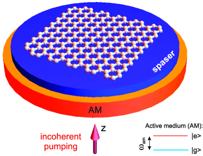
In the present paper graphene quantum amplifier, see Fig. 1, is consistently described. It is considered as an open quantum system. Below the graphene layer there is active medium (AM) layer with active molecules pumped incoherently. In Fig. 1 we schematically show the working two levels of the active molecule. Using quantum model we explore below how principal characteristics of the quantum amplifier develop with tuning of controlling parameters.
For simplicity we suppose that each particle or QD of active medium is multi-level system with “working” transition frequency . Also we assume that active medium with frequency interacts only with one mode of surface plasmon with the wavelength . After second quantization procedure plasmon energy spectrum are harmonic oscillator Fock states , where is number of excited plasmons.
If we focus on the working frequency then each active medium active atom can be effectively described by the two-level system with excited and ground states, see Fig. 1.
Graphene plasmons are investigated in the range so the mean value of thermal boson number in reservoirs at room temperature. So the system dynamics in the Markovian approximation can be described by the Lindblad equation Carmichael (2008):
| (1) |
Here is the density matrix of the whole “plasmon + active medium” system which Hilbert space is the direct product of the plasmon and two-level atoms Hilbert spaces. The first term in the right-hand side of (1) describes hermitian Hamiltonian dynamics, where consists of three contributions: Hamiltonian of plasmon, two-level system and the interaction between them. Here and are plasmon creation and annihilation operators, respectively, and are the transition operators of -th two-level atom, is the Rabi constant of the interaction between plasmon and active medium, is the surface plasmon frequency. As we mentioned above during calculation we suppose . Second term is the Lindblad part corresponding to the plasmon damping with the rate . Third and fourth terms correspond to energy decay with the rate and dephasing with the rate (also known as longitudinal and transverse relaxations). Finally, last term is responsible for incoherent pumping of two-level atom with the rate .
Note that we neglect interaction between two-level particles. This may be justified when interaction between each atom and surface plasmon is much larger than interaction between atoms. If so, interaction between atoms results in energy dissipation and redifinition of pumping rates.
Suppose that there is no frequency mismatch between atomic dipole moments. This is true when all atoms occupy subwavelength volume or distance between them is of the order of plasmon wavelength. So all atoms may be considered as identical and it is possible to introduce collective atomic operator , , and . With the aid of these operators and the assumption that all atoms are identical it is possible to rewrite Eq. (1) in the form
| (2) |
where the Lindbladian, .
The form of Eq. (2) is standard, but important are specific values of the damping and pumping rates. The damping rates of surface plasmon and Rabi constant are controlling parameters. The value of damping constant of semiconductor active medium may be evaluated as follows: , Khurgin and Sun (2012a, b). The value of the pumping rate is experimentally controllable parameter. Its maximal value strongly depends on the type of active medium. In Refs. Khurgin and Sun (2012a, b) it has been shown that the pumping rate corresponds to the current density which is nearly the maximal achievable value of current density today in semiconductors. For colloidal quantum dots and dye molecles which are pumped by external electromagnetic field corresponding field intensity is Andrianov et al. (2013). We take in our model the value, , as maximum possible pumping rate .
III Numerical estimation of the main parameters, Rabi constant () and plasmon decay rate ()
III.1 Rabi constant
To calculate interaction constant between plasmon field and graphene we use standard relation
| (3) |
where is matrix element of dipole moment, E is the field amplitude. It can be determined from the Helmholtz equation
| (4) |
and normalized through
| (5) |
Note that
| (6) |
In the structure under study, see Fig. 1, the permittivity essentially depends on coordinate. At it is equal to the permittivity of the substrate, at it is equal to the surface permittivity of graphene: , where is the Dirac delta function and is the graphene surface conductivity; at the permittivity is equal to unity. Finally we have
| (7) |
where is permittivity of the dielectric substrate, is the area of graphene nanoflake, is the tangential component of electric field, subscript denotes the value at on graphene layer.
Let and are the imaginary parts of the normal components of surface plasmon wave vectors in vacuum and dielectric correspondingly. So and , where is the surface plasmon wave number and .
Electric field depends on as follows: in dielectric () and in vacuum (). Then
| (8) |
Finally, let us note the relation between the tangential and normal electric field components: in vacuum and in dielectric. Along with the relation , we find in vacuum and in dielectric. For plasmon in graphene, , which means . In the same approximation, , which leads to
| (9) |
Using this equation and relation (5) we transform (3) into
| (10) |
where we take into account that to satisfy resonant condition. Conductivity for graphene layer may be expressed as Falkovsky (2008); Kotov et al. (2013):
| (11) | ||||
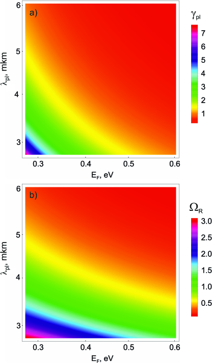
So from (10) and (11) we obtain the dependence of Rabi constant on the plasmon frequency and Fermi energy, see Fig. 2.
III.2 Plasmon decay rate
The plasmonic mode relaxation rate due to Joule losses is introduced as Landau et al. (1984); Novotny and Hecht (2012)
| (12) |
Using the relations (5) and (6) and taking into account that we obtain
| (13) |
So, we have found the dependence of Rabi constant of interaction between plasmon field and active medium, and plasmon relaxation rate as function of and .
IV Transition from enhanced spontaneous emission to lasing
Now we investigate the generation of surface plasmon and its coherent properties using parameters determined in the previous section. First we should note that all the equations derived above are applicable when the Fermi level is in the range and plasmon wavelength : otherwise we should take into account intraband transitions in graphene stimulated pumping. Doing numerical calculation we see that the Rabi constant and the damping rate have qualitatively the same behavior: they decrease as the functions of and , see Fig. 2.
Now we will investigate the graphene nanolaser dynamics. For this we solve master equation (1) changing parameters and .
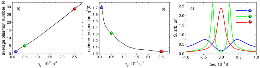
Sometimes it is a difficult question how to distinguish lasing from highly coherent fluorescence. There are several important observables describing the transition to lasing behavior Haken (1983); Siegman (1971); Khanin (2005); Chow et al. (2014). The first one is the dependence of the plasmon number on the pumping rate in double logarithmic scale. “S” shape of such curve indicates the first lasing threshold. (There are in fact threshholdless lasers with no pronounced lower threshold Protsenko (2012); Protsenko et al. (1999, 2005).) The second characteristic is the dependence of the second order correlation function, . When we have Poisson photon statistics; usually in lasing systems this case corresponds to coherent photon state. If then the photon state is “incoherent” and statistics is super-Poisson. If then statistics is sub-Poison.
One more characteristics which we will use is spectrum of the generated plasmon, namely, . Narrowing of the spectral line may be interpreted as increasing of coherence. The value of pumping rate corresponding to narrowing of the spectral line width we refer to as the second threshold.
Doing numerical calculations we assume that the number of two-level particles of active medium which interact with plasmonic mode is . This is so because the characteristic length of the graphene sheet and the size of usual mid-IR quantum dots is about nm and distance between them is the same order.
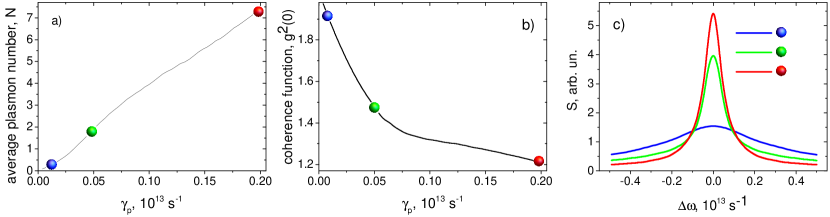
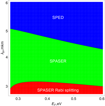
There are three different regimes. The first one corresponds to the high plasmon wavelength, namely, . The second regime corresponds to . In the third case we have .
In the first regime, see Fig. 3, we have thresholdless behavior of the plasmon number on pumping, whereas the does not approach the unity. At the same time, line narrowing is not pronounced. In this case we have enhanced spontaneous excitation of surface plasmon rather then stimulated emission of them. Device based on noncoherent generation of surface plasmons may be named as surface plasmon emitting diode Khurgin and Sun (2014) in analogous with light emitting diode in optical case.
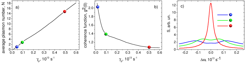
At second stage, see Fig. 4, we obtain thresholdless behavior of the plasmon number which indicates that there is relatively large number of plasmons excited by spontaneous transitions in active medium. So the dependence of the plasmon number on pumping does not indicate any coherence. However, other characteristics exhibit coherence explicitly: tends to unity and spectral line strongly narrows at the same time. These characteristics indicate the possibility of generation of coherent plasmons. So, in this case we have SPASER - surface plasmon generator by stimulated emission of radiation.
Third regime, see Fig. 5, is very similar to the previous one: tends to unity. However, line narrowing demonstrates one interesting feature. At moderate values of pumping we have doublet structure with two narrow lines. This happens due to high value of Rabi frequency at low value of surface plasmon wavelength. We name this regime as SPASER with Rabi spliting.
In Fig. 6 we summarize the main results. So, we consider three different regimes: SPED (surface plasmon emitting diode), when there is high value of spontaneous emission, SPASER (surface plasmon amplification by stimulated emission of radiation) regime, at which there is possible to obtain coherence at realistic pump rates and SPASER with Rabi splitting which is characterized by two narrow line of spectrum.
Note that for each plasmon wavelength it is necessary to use appropriate active medium with suitable transition frequency between working levels. Good candidates for this purpose are various types of quantum dots. For example, for SPASER and SPASER Rabi splitting regime PbSe Pietryga et al. (2004); Wehrenberg et al. (2002) and HgTe colloidal quantum dots Keuleyan et al. (2011); Lhuillier et al. (2013) as well as dopped ZnS, ZnSe, CdSe Mirov et al. (2010), dopped ZnSe, CdMnTe Mirov et al. (2010), SiGe quantum dots Wang et al. (2007), InGaAs/GaAs quantum box structure Botez (2007) and transition-metal-doped nanocrystalline quantum dots Mirov et al. (2007) may be used. For SPED regime HgTe colloidal quantum dots and transition-metal-doped nanocrystalline quantum dots (QD) is also appropriate. We summarize these data in Table 1.
| , | Type of active medium |
|---|---|
| 1.5 - 5 | HgTe colloidal QDs Keuleyan et al. (2011); Lhuillier et al. (2013) |
| 2 - 4 | PbSe colloidal QDs Pietryga et al. (2004); Wehrenberg et al. (2002) |
| 2.5 | dopped ZnS, ZnSe, CdSe Mirov et al. (2010) |
| 3 - 5 | Transition-metal-doped nanocrystalline QDs Mirov et al. (2007) |
| 3.5 | SiGe QDs Wang et al. (2007) |
| 4.5 | dopped ZnSe, CdMnTe Mirov et al. (2010) |
| 4.7 | InGaAs/GaAs quantum box structure Botez (2007) |
V Conclusions
In conclusion, we have shown doing self-consistent quantum calculations that graphene is the promising material for applications in state-of-the-art active and passive plasmonic devices that allow in situ tuning of parameters. High graphene conductivity dependence on Fermi-level and frequency allows switching between such generation types such as SPED and SPASER (surface plasmon amplification by stimulated emission of radiation). Corresponding generation spectrum and the second order correlation function which predicts laser statistics have been calculated. We provide explicit expressions for interaction and dissipation parameters through material constants and geometry.
Acknowledgements.
The work was partially funded by Russian Foundation for Scientific Research (grant No.16-02-00295), while numerical simulations were funded by Russian Scientific Foundation (grant No.14-12-01185). We thank Supercomputer Centers of Russian Academy of Sciences and National research Center Kurchatov Institute for access to URAL, JSCC and HPC supercomputer clusters.References
- Maier (2007) S. A. Maier, Plasmonics: fundamentals and applications (Springer Science & Business Media, 2007).
- Shvets and Tsukerman (2011) G. Shvets and I. Tsukerman, Plasmonics and Plasmonic Metamaterials: Analysis and Applications, Vol. 4 (World Scientific, 2011).
- Enoch and Bonod (2012) S. Enoch and N. Bonod, Plasmonics: from basics to advanced topics, Vol. 167 (Springer, 2012).
- Zouhdi et al. (2008) S. Zouhdi, A. Sihvola, and A. P. Vinogradov, Metamaterials and Plasmonics: Fundamentals, Modelling, Applications (Springer Science & Business Media, 2008).
- Bozhevolnyi (2006) S. Bozhevolnyi, “Plasmonic nanoguides and circuits. 2008,” (2006).
- Shalaev and Kawata (2006) V. M. Shalaev and S. Kawata, Nanophotonics with surface plasmons (Elsevier, 2006).
- Zayats and Maier (2013) A. V. Zayats and S. Maier, Active plasmonics and tuneable plasmonic metamaterials, Vol. 8 (John Wiley & Sons, 2013).
- Sarychev and Shalaev (2007) A. K. Sarychev and V. M. Shalaev, Electrodynamics of metamaterials (World Scientific, 2007).
- West et al. (2010) P. R. West, S. Ishii, G. V. Naik, N. K. Emani, V. M. Shalaev, and A. Boltasseva, Laser & Photonics Reviews 4, 795 (2010).
- E. and V. (1987) L. Y. E. and K. A. V., The dielectric function and collective oscillations inhomogeneous systems (ed. by Keldysh, L. V. and Kirzhnits D. A. and Maradudin A. A., North Holland: Amsterdam, 1987).
- Ji et al. (2007) A.-C. Ji, X. C. Xie, and W. M. Liu, Phys. Rev. Lett. 99, 183602 (2007).
- Barnes et al. (2003) W. L. Barnes, A. Dereux, and T. W. Ebbesen, Nature 424, 824 (2003).
- Radko et al. (2008) I. P. Radko, A. B. Evlyukhin, A. Boltasseva, and S. I. Bozhevolnyi, Opt. Exp. 16, 3924 (2008).
- Gong and Vučković (2007) Y. Gong and J. Vučković, Appl. Phys. Lett. 90, 033113 (2007).
- Archambault et al. (2009) A. Archambault, T. V. Teperik, F. Marquier, and J.-J. Greffet, Phys. Rev. B 79, 195414 (2009).
- Feng et al. (2007) L. Feng, K. A. Tetz, B. Slutsky, V. Lomakin, and Y. Fainman, Appl. Phys. Lett. 91, 081101 (2007).
- Zia and Brongersma (2007) R. Zia and M. L. Brongersma, Nat. Nanotechnology 2, 426 (2007).
- Pockrand et al. (1978) I. Pockrand, J. Swalen, J. Gordon, and M. Philpott, Surface Science 74, 237 (1978).
- Mills and Agranovich (1982) D. L. Mills and V. M. Agranovich, Surface Polaritons: Electromagnetic Waves at Surfaces and Interfaces (North-Holland publ., 1982).
- Mulvaney (1996) P. Mulvaney, Langmuir 12, 788 (1996).
- Eberlein et al. (2008) T. Eberlein, U. Bangert, R. Nair, R. Jones, M. Gass, A. Bleloch, K. Novoselov, A. Geim, and P. Briddon, Phys. Rev. B 77, 233406 (2008).
- Tanaka et al. (2013) R. Tanaka, R. Gomi, K. Funasaka, D. Asakawa, H. Nakanishi, and H. Moriwaki, Analyst 138, 5437 (2013).
- Jeanmaire and Van Duyne (1977) D. L. Jeanmaire and R. P. Van Duyne, J. Electroanalytical Chemistry and Interfacial Electrochemistry 84, 1 (1977).
- Otto (1978) A. Otto, Surface Science 75, L392 (1978).
- Eesley (1981) G. Eesley, Phys. Rev. B 24, 5477 (1981).
- Tsang et al. (1979) J. Tsang, J. Kirtley, and J. Bradley, Phys. Rev. Lett. 43, 772 (1979).
- Fang et al. (2013) C. Fang, D. Brodoceanu, T. Kraus, and N. H. Voelcker, Rsc Advances 3, 4288 (2013).
- Cao et al. (2002) Y. C. Cao, R. Jin, and C. A. Mirkin, Science 297, 1536 (2002).
- Ang et al. (2015) S. H. Ang, M. Thevarajah, Y. Alias, and S. M. Khor, Clinica Chimica Acta 439, 202 (2015).
- Hawrylak and Quinn (1986) P. Hawrylak and J. J. Quinn, Appl. Phys. Lett. 49, 280 (1986).
- Kempa et al. (1988) K. Kempa, P. Bakshi, and J. Cen, in 1988 Semiconductor Symposium (International Society for Optics and Photonics, 1988) pp. 62–67.
- Maier (2006) S. A. Maier, Optics communications 258, 295 (2006).
- Sirtori et al. (1998) C. Sirtori, C. Gmachl, F. Capasso, J. Faist, D. L. Sivco, A. L. Hutchinson, and A. Y. Cho, Opt. Lett. 23, 1366 (1998).
- Tredicucci et al. (2000) A. Tredicucci, C. Gmachl, F. Capasso, A. F. Hutchinson, D. L. Sivco, and A. Y. Cho, Appl. Phys. Lett. 76, 2164 (2000).
- Babuty et al. (2010) A. Babuty, A. Bousseksou, J.-P. Tetienne, I. M. Doyen, C. Sirtori, G. Beaudoin, I. Sagnes, Y. De Wilde, and R. Colombelli, Phys. Rev. Lett. 104, 226806 (2010).
- Oulton et al. (2009) R. F. Oulton, V. J. Sorger, T. Zentgraf, R.-M. Ma, C. Gladden, L. Dai, G. Bartal, and X. Zhang, Nature 461, 629 (2009).
- Noginov et al. (2008) M. A. Noginov, G. Zhu, M. Mayy, B. A. Ritzo, N. Noginova, and V. A. Podolskiy, Phys. Rev. Lett. 101, 226806 (2008).
- Bergman and Stockman (2003) D. J. Bergman and M. I. Stockman, Phys. Rev. Lett. 90, 027402 (2003).
- Protsenko et al. (2005) I. E. Protsenko, A. V. Uskov, O. Zaimidoroga, V. Samoilov, and E. O reilly, Phys. Rev. A 71, 063812 (2005).
- Andrianov et al. (2012) E. Andrianov, A. Pukhov, A. Dorofeenko, A. Vinogradov, and A. Lisyansky, Phys. Rev. B 85, 165419 (2012).
- Andrianov et al. (2011a) E. Andrianov, A. Pukhov, A. Dorofeenko, A. Vinogradov, and A. Lisyansky, Opt. Express 19, 24849 (2011a).
- Andrianov et al. (2011b) E. Andrianov, A. Pukhov, A. Dorofeenko, A. Vinogradov, and A. Lisyansky, Opt. Lett. 36, 4302 (2011b).
- Noginov et al. (2009) M. Noginov, G. Zhu, A. Belgrave, R. Bakker, V. Shalaev, E. Narimanov, S. Stout, E. Herz, T. Suteewong, and U. Wiesner, Nature 460, 1110 (2009).
- Lu et al. (2012) Y.-J. Lu, J. Kim, H.-Y. Chen, C. Wu, N. Dabidian, C. E. Sanders, C.-Y. Wang, M.-Y. Lu, B.-H. Li, X. Qiu, et al., Science 337, 450 (2012).
- Hill et al. (2009) M. T. Hill, M. Marell, E. S. Leong, B. Smalbrugge, Y. Zhu, M. Sun, P. J. van Veldhoven, E. J. Geluk, F. Karouta, Y.-S. Oei, et al., Opt. Express 17, 11107 (2009).
- Suh et al. (2012) J. Y. Suh, C. H. Kim, W. Zhou, M. D. Huntington, D. T. Co, M. R. Wasielewski, and T. W. Odom, Nano Lett. 12, 5769 (2012).
- van Beijnum et al. (2013) F. van Beijnum, P. J. van Veldhoven, E. J. Geluk, M. J. de Dood, W. Gert, and M. P. van Exter, Phys. Rev. Lett. 110, 206802 (2013).
- Berini and De Leon (2012) P. Berini and I. De Leon, Nat. Photonics 6, 16 (2012).
- Tame et al. (2013) M. Tame, K. McEnery, Ş. Özdemir, J. Lee, S. Maier, and M. Kim, Nat. Physics 9, 329 (2013).
- Ju et al. (2011a) L. Ju, B. Geng, J. Horng, C. Girit, M. Martin, Z. Hao, H. A. Bechtel, X. Liang, A. Zettl, Y. R. Shen, et al., Science 334, 463 (2011a).
- Ju et al. (2011b) L. Ju, B. Geng, J. Horng, C. Girit, M. Martin, Z. Hao, H. A. Bechtel, X. Liang, A. Zettl, Y. R. Shen, et al., Nat. Nanotechnology 6, 630 (2011b).
- Koppens et al. (2011) F. H. Koppens, D. E. Chang, and F. J. Garcia de Abajo, Nano Lett. 11, 3370 (2011).
- Grigorenko et al. (2012) A. Grigorenko, M. Polini, and K. Novoselov, Nat. Photonics 6, 749 (2012).
- Garcia de Abajo (2014) F. J. Garcia de Abajo, ACS Photonics 1, 135 (2014).
- Low and Avouris (2014) T. Low and P. Avouris, ACS Nano 8, 1086 (2014).
- Maier (2012) S. A. Maier, Nat. Phys. 8, 581 (2012).
- Novoselov et al. (2005) K. Novoselov, A. K. Geim, S. Morozov, D. Jiang, M. Katsnelson, I. Grigorieva, S. Dubonos, and A. Firsov, Nature 438, 197 (2005).
- Zhang et al. (2005) Y. Zhang, Y.-W. Tan, H. L. Stormer, and P. Kim, Nature 438, 201 (2005).
- Bolotin et al. (2008) K. I. Bolotin, K. Sikes, Z. Jiang, M. Klima, G. Fudenberg, J. Hone, P. Kim, and H. Stormer, Solid State Comm. 146, 351 (2008).
- Balandin et al. (2008) A. A. Balandin, S. Ghosh, W. Bao, I. Calizo, D. Teweldebrhan, F. Miao, and C. N. Lau, Nano Lett. 8, 902 (2008).
- Hwang and Sarma (2007) E. Hwang and S. D. Sarma, Phys. Rev. B 75, 205418 (2007).
- Otsuji et al. (2014) T. Otsuji, V. Popov, and V. Ryzhii, J. Phys. D: Appl. Phys. 47, 094006 (2014).
- Berman et al. (2013) O. L. Berman, R. Y. Kezerashvili, and Y. E. Lozovik, Physical Review B 88, 235424 (2013).
- Rupasinghe et al. (2014) C. Rupasinghe, I. D. Rukhlenko, and M. Premaratne, ACS Nano 8, 2431 (2014).
- Apalkov and Stockman (2014) V. Apalkov and M. I. Stockman, Light: Science & Applications 3, e191 (2014).
- Carmichael (2008) H. J. Carmichael, Statistical methods in quantum optics, Vol. 2 (Springer, 2008).
- Khurgin and Sun (2012a) J. B. Khurgin and G. Sun, Optics Express 20, 15309 (2012a).
- Khurgin and Sun (2012b) J. B. Khurgin and G. Sun, Appl. Phys. Lett. 100, 011105 (2012b).
- Andrianov et al. (2013) E. Andrianov, D. Baranov, A. Pukhov, A. Dorofeenko, A. Vinogradov, and A. Lisyansky, Optics express 21, 13467 (2013).
- Falkovsky (2008) L. A. Falkovsky, Physics-Uspekhi 51, 887 (2008).
- Kotov et al. (2013) O. Kotov, M. Kol’chenko, and Y. E. Lozovik, Optics express 21, 13533 (2013).
- Landau et al. (1984) L. D. Landau, J. Bell, M. Kearsley, L. Pitaevskii, E. Lifshitz, and J. Sykes, Electrodynamics of continuous media, Vol. 8 (elsevier, 1984).
- Novotny and Hecht (2012) L. Novotny and B. Hecht, Principles of nano-optics (Cambridge university press, 2012).
- Haken (1983) H. Haken, Laser theory (Springer-Verlag, New York, NY, USA, 1983).
- Siegman (1971) A. E. Siegman, (1971).
- Khanin (2005) Y. I. Khanin, Fundamentals of laser dynamics (Cambridge Int Science Publishing, 2005).
- Chow et al. (2014) W. W. Chow, F. Jahnke, and C. Gies, Light Sci. Appl. 3, e201 (2014).
- Protsenko (2012) I. E. Protsenko, Physics-Uspekhi 55, 1040 (2012).
- Protsenko et al. (1999) I. Protsenko, P. Domokos, V. Lefèvre-Seguin, J. Hare, J. Raimond, and L. Davidovich, Phys. Rev. A 59, 1667 (1999).
- Khurgin and Sun (2014) J. B. Khurgin and G. Sun, Nat. Photonics 8, 468 (2014).
- Pietryga et al. (2004) J. M. Pietryga, R. D. Schaller, D. Werder, M. H. Stewart, V. I. Klimov, and J. A. Hollingsworth, Journal of the American Chemical Society 126, 11752 (2004).
- Wehrenberg et al. (2002) B. L. Wehrenberg, C. Wang, and P. Guyot-Sionnest, J. Phys. Chem. B 106, 10634 (2002).
- Keuleyan et al. (2011) S. Keuleyan, E. Lhuillier, and P. Guyot-Sionnest, Journal of the American Chemical Society 133, 16422 (2011).
- Lhuillier et al. (2013) E. Lhuillier, S. Keuleyan, H. Liu, and P. Guyot-Sionnest, Chem. Mater. 25, 1272 (2013).
- Mirov et al. (2010) S. B. Mirov, V. V. Fedorov, I. S. Moskalev, D. V. Martyshkin, and S. Kim, Laser and Photon. Rev. 4, 21 (2010).
- Wang et al. (2007) K. L. Wang, D. Cha, J. Liu, and C. Chen, Proceedings of the IEEE 95, 1866 (2007).
- Botez (2007) D. Botez, International Journal of Nanoscience 6, 203 (2007).
- Mirov et al. (2007) S. B. Mirov, V. V. Fedorov, I. S. Moskalev, and D. V. Martyshkin, IEEE Journal of Selected Topics in Quantum Electronics 13, 810 (2007).