Mechanisms for p-type behavior of ZnO, Zn1-xMgxO and related oxide semiconductors
Abstract
Possibilities of turning intrinsically n-type oxide semiconductors like ZnO and Zn1-xMgxO into p-type materials are investigated. Motivated by recent experiments on Zn1-xMgxO doped with nitrogen we analyze the electronic defect levels of point defects NO, vZn, and NO-vZn pairs in ZnO and Zn1-xMgxO by means of self-interaction-corrected density functional theory calculations. We show how the interplay of defects can lead to shallow acceptor defect levels, although the levels of individual point defects NO are too deep in the band gap for being responsible for p-type conduction. We relate our results to p-type conduction paths at grain boundaries seen in polycrystalline ZnO and develop an understanding of a p-type mechanism which is common to ZnO, Zn1-xMgxO, and related materials.
pacs:
71.23.-k,71.55.Jv,71.20.MqI Introduction
Zinc oxide is a prominent example of an intrinsically n-type semiconductor. Its abundant availability, its low-cost production, and its wide electronic band gap of approximately 3.4 eV make ZnO attractive for transparent and conducting oxide layers in consumer-electronics devices. However, a break-through of ZnO-based transparent electronics has not been achieved so far due to the lack of sufficiently conductive and long-term stable p-type ZnO layers. The problem of p-type doping of ZnO has by now been a scientific challenge for more than two decades. Besides the doping with single elements like N, P, As, or Sb, substituting O and Li, Na, K, Cu, Ag or Au, substituting Znle01 ; le04 ; le06 ; pa02 ; li04 ; ya08 co-doping was discussed as well.wa03 ; zha06 ; ya07 Apparently, the most promising candidate so far is still nitrogen. However, it was shown theoreticallyly09 ; la10 ; ko10 that the substitutional defect of N on O sites (NO) cannot be responsible for the p-type conduction which has been observed in some experiments,re13 since it creates a defect level which is located too high above the valence band (VB) edge with respect to thermal excitation energies.
Recent theoretical and experimental studies consider more complicated defect complexes which involve zinc vacancies (vZn) or co-doping, like the NO-vZn or NO-vZn-H defect complexes, as potential sources of p-type conduction.liu12 ; am15
For polycrystalline ZnO it has been proposed that conduction channels of p-type can be found along grain boundaries.wa09 ; ko10 Here it is an interplay of grain boundaries, their depletion regions, and point defects that results in the desired low lying acceptor levels.
It has been reported by Hierro et al.hi09 that the use of ternary ZnO-based alloys like Zn1-xMgxO (denoted by ZMO in the following) facilitates the p-type conductivity due to lower net electron concentrations than in pure ZnO. These authors relate the reduced net electron concentration to two deep lying Mg-related defects which act as electron traps. ZMO retains the wurtzite crystal structure of ZnO for Mg substituting Zn for concentrations up to , and also the lattice parameters change only slightly. Hence combining ZMO with n-type ZnO layers leads to negligible lattice misfits.hi09
Up to now it is not yet clear which atomic or extended defects provide the key to promote p-type conductivity in ZnO and related materials like ZMO. An understanding of this defect physics would allow a targeted development of experimental routes to synthesize materials having these particular acceptor states.
In this paper we present a density functional theory (DFT) study determining the electronic defect levels of the defects NO, vZn, and NO-vZn in ZnO and ZMO. We discuss our results in the context of the accumulated experimental and theoretical knowledge, and thereby we shed light on the question of why some experimental routes recently taken have lead to p-conduction but others not. Are the defect states that originate from NO indeed too deeply09 ; ko10 in the band gap? What changes when NO forms a defect complex with a Zn vacancy, and how do Mg atoms nearby affect its defect level position? For the determination of the electronic defect levels we use a self-interaction corrected (SIC) local-density approximation (LDA) approachko10 that is capable to give far better results than both commonly used approximations, the LDA and the generalized gradient approximation (GGA). The latter two have limited predictive power for wide band gap semiconductors due to their inherent significant underestimation of the band gap due to their self-interaction error. SIC–LDA overcomes this limitation and yields electronic band structures with band gaps that are in good agreement with experimentko10 ; ko11 and in particular for ZnO a correct separation of the Zn-3d and O-2p bands.ko14 By means of this approach, the defect levels in various amorphous oxide semiconductors based on In, Sn, and Zn have been predicted reliably.sa14 ; sa15 ; ko13 ; ko15
The results presented in this paper may solve the controversial problem that individual NO defects are indeed creating levels lying too deep inside the band gap even though nitrogen doping has been observed to lead to p-type ZnO and ZMO, probably due to an interplay with other defects. Moreover, we relate our present results to the p-type conduction effects which have been observed for grain boundaries in ZnO, and we relate all this to one common origin. The emerging theoretical picture will presumably be useful for the experimental optimization of p-type conduction in ZnO and ZMO.
II Computational approach
II.1 Supercell models
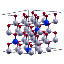
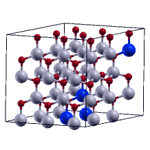
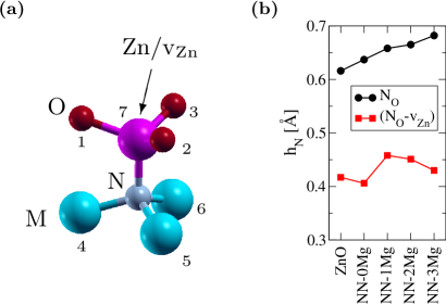
For the study of defect complexes we have chosen a supercell model of the wurtzite crystal structure of ZnO containing 72 atoms and consisting of primitive unit cells. Since Zn1-xMgxO retains the wurtzite structure for Mg concentrations %hi09 the corresponding supercells were generated by randomly substituting Zn atoms by Mg atoms. For the study of the bulk crystal properties like lattice parameters and band gap as function of the Mg concentration we compared several realizations of random Mg distributions within the 72-atoms supercell, and we find a negligible dependency of these properties on the Mg distribution. For comparison, we have also examined results from a 36-atom supercell in the study of bulk properties. For the subsequent study of defects we have chosen the specific Mg concentration of 11% (i.e. replacing 4 of 36 Zn atoms by Mg atoms in the 72-atom supercell) which is representative for typical experimental concentrations.ku14 Furthermore, the defect analysis concentrates on specific realizations of the Mg distribution which differ in the number of Mg atoms that cluster in the direct neighborhood of the -point defect under study. Two such realizations are displayed in Fig. 1.
II.2 Structure optimization
The structure optimization of all the constructed supercell models was carried out using the projector augmented-wave (PAW) methodbl94 as implemented in the VASP code.kr96 ; kr99 The LDA was used for the exchange-correlation functional, and PAW potentials describing the Zn-(3d,4s,4p), Mg-3s, and O-(2s,2p) as valence electrons. All VASP calculations were carried out with a plane-wave cutoff energy of 400 eV, a Monkhorst-Pack k-mesh, and a Gaussian broadening of 0.1 eV.
For all bulk structures the volume optimization was carried out by fitting the universal equation of statero81 to a dataset of minimal total energies calculated at different cell volumes. Optimization of the lattice parameter ratio c/a and internal relaxation of the atomic positions were achieved by minimizing the elastic stress and the forces acting on the atoms, respectively. The supercells containing defects were internally relaxed at fixed volume and c/a ratio.
II.3 Electronic-structure calculations
The electronic-structure calculations on the basis of the SIC-LDA were performed using the computational mixed-basis pseudopotential (MBPP) methodel90 ; el92 ; lech04 ; mey95 with the same calculation setup as reported in previous papers.ko10 ; ko11b ; ko11c We have taken the LDA for exchange-correlation as parametrized by Perdew and Zunger.pe81 For Zn, Mg, and O optimally smooth norm–conserving pseudopotentialsva85 were constructed, and a mixed basis of plane waves and non-overlapping localized orbitals were used. Due to the localized orbitals a plane–wave cutoff energy of 20 Ry (1Ry = 13.606 eV) is sufficient for obtaining well converged results. For the k-point sampling of the Brillouin-zone integrals a Monkhorst-Pack mesh of and a Gaussian broadening of 0.2 eV were used. The DOS of the supercells were evaluated with the same mesh and a Gaussian broadening of 0.1 eV.
The self-interaction of the LDA is corrected by an incorporation of the SIC in the pseudopotentials.vo96 ; ko10 The SIC procedure uses weight factors accounting for the occupations of the individual s, p and d valence orbitals. We corrected the Zn 3d semicore-orbitals by 100%, i.e. Zn=(0, 0, 1). The localized O-2s semi-core orbitals are also corrected by 100% while for the spatially more extended O-2p valence-band orbitals we have taken 80% which implies the weight factors O=(1, 0.8, 0). We did not apply a SIC to the almost unoccupied Mg-3s, 3p and Zn-4s, 4p conduction-band orbitals of the almost fully ionic compounds Zn1-xMgxO. For the adjustment of the atomic SIC to the crystal field in the solids, a scaling factor is applied.
III Results and discussion
III.1 Lattice parameters
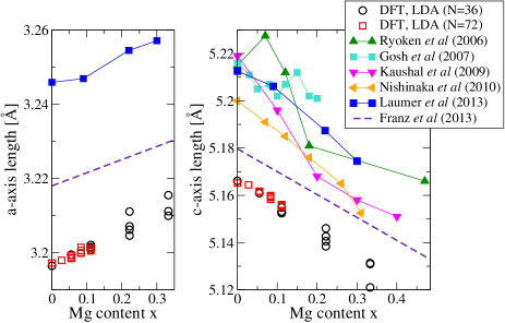
The functional dependencies of the lattice parameters and on the Mg content are displayed in Fig. 2. Our results underestimate the experimental values by about one percent, which is a typical systematic deviation for LDA results. The increase of and the decrease of with increasing Mg content are quantitatively correct and just slightly shifted with respect to previous experimentalry06 ; gh07 ; kau09 ; nish10 ; lau13 and theoreticalfranz13 findings. This good agreement on the structural parameters is the prerequisite for the electronic structure calculations which are the focus of this work. Note that the deviations from Vegard’s rule in some of the values of the experimentally observed lattice constants is probably related to the quality of the thin films and maybe due to the presence of compensated defects or residual strain as discussed, e.g., by Ryoken et al.ry06
III.2 Band gap of ZMO
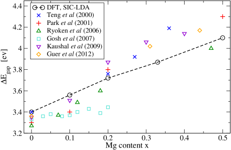
Theoretical and experimental values of the band gap of Zn1-xMgxO as function of the Mg content are displayed and compared in Fig. 3. The results obtained by the SIC-LDA approach do not only show the rising trend correctly, but also the calculated values agree quantitatively well to the experimental data. The dependency of the band gap on the specific distribution of Mg atoms within the supercell is small, e.g. for the sample structures with we find an energy scatter of only meV.
The wide scatter of experimental results in Fig. 3 is probably due to the varying quality of the thin films but also due to different experimental approaches of determining the band gaps.te00 ; pa01 ; ry06 ; gh07 ; gu12 Above the thermodynamical solubility limit of a non-equilibrium solid solution is formed. Depending on the route of synthesis, this results in compositional non-uniformity which then leads to the generation of non-equilibrium compensated defectsgh07 or even structural inhomogeneityry06 and residual elastic stress. Naturally, all of this is reflected in the measured physical properties of the films, as discussed in the respective articles.
For our investigation the calculation of the band gap as function of the Mg content serves as a validation that the SIC-LDA describes the electronic structure of the Zn-Mg-O system rather well.
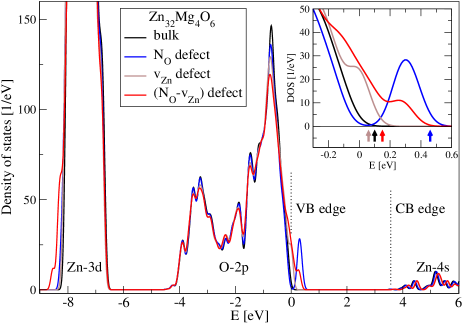
The total density of states (DOS) of a representative Zn32Mg4O36 sample calculated with the SIC-LDA approach is shown in Figure 4. The upper part of the VB is mainly formed by the O 2p valence orbitals while the lower part is dominated by the Zn 3d semicore orbitals. Experimentally, the average d-band energy of ZnO was determined to be at -7.8 eV relative to the VB edge.he82 This is almost unchanged when Mg is introduced. The SIC-LDA approach reproduces this experimental observation in contrast to LDA, GGA and several commonly used hybrid functionals which place the Zn 3d levels too high in energy and therefore overestimate their hybridization with the O 2p levels. The latter can lead to wrong positions of defect levels in the band gap.ko14 Thus these results validate our approach to analyze individual electronic levels of point defects by using the SIC-LDA approach.
III.3 Electronic defect levels near the VB
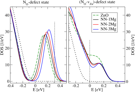
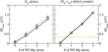
From the total density of states (DOS) in Fig. 4 it can be seen that the defects NO, vZn and NO-vZn create energy levels close the VB edge. However, a closer inspection – which is provided in the inset – shows that the defect levels that originate from NO are separated from the VB with a peak at about 0.25 eV. In the left panel of Fig. 5 the position of the NO defect level is shown as function of the number of nearest Mg neighbors (NN). Here, NN-1Mg indicates a Zn32Mg4O35N (or Zn31Mg4O35N) supercell in which one Mg atom is adjacent to the NO (or NO-vZn) defect, respectively, while in the NN-2Mg and NN-3Mg supercells, two and three Mg atoms are nearest neighbors of the defect.
An increasing number of NN Mg atoms leads to an up-shift of the defect level. Therefore, concerning p-type conductivity, Mg doping makes NO defects less attractive since the level becomes more narrow and moves deeper into the band gap. On the other hand, the energy level position of the NO-vZn defect complex remains almost unchanged for different numbers of NN Mg atoms.
The substitution of Zn by Mg in ZnO does not help to make the acceptor levels of individual NO defects shallow, which would facilitate p-type conductivity at room temperature, but rather provokes the contrary. Moreover, it has been reportedgai08 that the presence of Mg atoms in the neighborhood of a NO defect increases the defect formation energy considerably and therefore reduces the respective defect concentration in the material. Our calculations are in line with the findings of Ref. gai08, , see discussion in the Appendix.
Zinc vacancy defects alone create very shallow defect levels (see inset of Fig. 4), which is a well known result from previous studies.ko11b Experimentally, defect levels at either 130meVre13 , 160 meVku14 , or 190 meVmu12 are reported, depending on the specific experiment. According to Fig. 5, the levels of the NO-vZn defect complex lie higher above the VB edge than that of the individual vZn defect and fit to the experimentally determined values rather well. We thus propose to assign the experimentally found acceptor levels to a NO-vZn defect complex. This complex is very promising since it provides shallow defect levels that are not separated in energy from the VB edge, and thus continuous low energy excitation are possible. The position of the defect level varies only slightly with the number of Mg atoms near the defect complex (see right panel of Fig. 5).
III.4 Spatial distribution of NO and NO-vZn defect levels
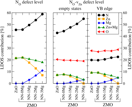
In order to analyze the spatial distribution of the defect levels we have evaluated the atom-projected local densities of states (LDOS) for the most relevant atoms involved in the defect (complex). Figure 6 displays their contributions to the defect levels while the relative locations of these atoms are sketched in Fig. 7a. A contribution of an individual neighbor atom to a defect level is evaluated by integrating the LDOS of the respective atom in the relevant energy interval and subsequent division by the sum of the LDOS of all atoms in the supercell, integrated for the same energy range. The energy interval [-0.1, 0.5]eV was chosen for the analysis of the NO defect, while the analysis of the NO-vZn defect complex is carried out separately for the intervals [-0.2, 0.0]eV (VB edge) and [0.0, 0.4]eV (unoccupied states above the VB edge), c.f. Fig. 5.
Note that the contributions for the oxygen ions (red line) and metal ions (green line) shown in Fig. 6 are the sums for the 3 O-atoms (numbered 1–3 in Fig. 7a) and the 3 or 4 metal atoms (numbered 4–7 in Fig. 7a), respectively. The metal atoms at positions 4–6 can be either Zn or Mg, while position 7 corresponds to either a Zn atom in the case of the NO defect or to a Zn vacancy, in the case of the NO-vZn defect complex.
The NO defect level is highly localized on the central N-atom, by more than , as can be seen from the left panel in Fig. 6. About is shared by the four NN metal atoms, while the oxygen atoms of the second neighbor shell contribute with or less each. The localization on the N-atom increases to with an increasing number of NN Mg-atoms, while the total contribution of the NN metal atoms remains rather constant. This increase in localization is connected to an increasing spatial separation of the N atom from the plane defined by the three metal atoms 4–6 with increasing number of Mg atoms therein, see graph in Fig. 7b.
The analysis of the spatial distribution of the NO-vZn defect (c.f. middle and right panel in Fig. 6) is divided into two parts, namely (i) the unoccupied states above the VB edge and (ii) the VB edge which is modified with respect to the bulk material by the presence of the defect. The unoccupied states (middle panel in Fig. 6) are reminiscent of the NO defect and the N atom contributes more than 40% in pure ZnO which increases up to 55% with increasing number of NN Mg. The hybridization with the vZn defect state results in a contribution of the three oxygen atoms next to the vacancy site. The three remaining NN metal atoms (numbered 4–6 in Fig. 7a) only contribute 2–3% (Zn) and 1% (Mg), each. For the VB edge (right panel in Fig. 6), reminiscent of the vZn defect, the 3 oxygen atoms are more important (27%), but the N-atom still contributes on average with 20%. A change in the number of NN Mg atoms has only little effect on this spatial distribution with a small shift of weight from the NN metal atoms to N.
III.5 Defect-complex mechanism for p-type conduction mechanism
For p-type conduction a Fermi level close the VB edge and shallow acceptor levels in sufficiently high concentration are needed. Since the thermal excitation energy at room temperature is only about 25 meV, p-type conduction with a significant hole concentration can at best be achieved by acceptor defect levels which are distributed continuously right above the VB edge. Our SIC-LDA analysis of the most relevant defects in N-doped ZMO shows that vZn and NO-vZn indeed provide such defect levels.
Our results support the hypothesis that co-doping of ZnO with Mg and N can be a possible route to obtain p-type conductivity. The (NO-vZn) defect complex yields shallow acceptor levels which can be activated by the experimentally reported lowering of the net electron concentration in ZMO.Li07 ; Qiu07 ; hi09 This carrier compensation effect increases linearly with the Mg content and can be explained by deep-lying Mg-related defects which act as charge traps.hi09
Zinc vacancies are low lying energy defects which exist also in pure ZnO.ko11b However, pure ZnO usually is an intrinsically n-type semiconductor since donor defects dominate. Only grain boundaries in polycrystalline ZnO may provoke p-type conducting filmswa09 under oxygen rich conditions. In general the addition of oxygen is thought to reduce the number of oxygen vacancies which are supposed to be the key donor defects. We believe that an understanding of the effect of oxygen addition has to be extended to take the grain boundaries into account. Under oxygen rich conditions the percentage of grain boundaries with undercoordinated oxygen atoms increases. In previous workko10 ; ko11 we have shown that such grain boundaries contribute shallow levels above the VB edge. These are an equivalent to the defect levels of vZn in bulk-like ZnO or ZMO discussed here, since the oxygen atoms at the grain boundaries are undercoordinated due to local Zn deficiencies. Furthermore, nitrogen at grain boundaries can form shallow defect levels which are very similar to those shown in Fig. 5 (see Fig. 11 in Ref. ko10, ). We argue therefore that all these shallow levels are activated due to the depletion zones near grain boundaries.wa09 ; al06 Zhang et al. interpret their experimental results along this line,zha06 and Wang et al. even suppose that oxygen excess causes the formation of a quasi two dimensional hole gas which could explain the very high mobilities seen in some experiments (see Ref. wa09, and references therein).
Putting all from above together, this rather general defect-complex mechanism for promoting p-type conductivity in ZnO, ZMO, and related materials emerges: defect complexes which are connected to the zinc vacancies in the bulk interior or at grain boundaries provide shallow defect levels which can serve as acceptor defects. The activation of these defects by lowering the net electron concentration is provided either by co-doping (e.g. N and Mghi09 ) or by depletion zones around grain boundaries.
IV Summary
We have studied the electronic densities of states of crystalline ZnO and Zn1-xMgxO with . We have shown that the SIC-LDA allows to calculate the electronic band gap as function of the Mg content and leads to quantitatively reasonable results with respect to experimental data.
We have determined the electronic defect levels which are generated by the introduction of NO substitutional defects. They are at 0.25 eV above the VB or higher. An increasing number of neighboring Mg atoms to the NO site shifts the defect level even deeper into the band gap. On the other hand, isolated vZn defects generate shallow levels attached to the VB edge. In combination with NO, the defect complex NO-vZn produces low lying defect levels which emerge continuously above the VB and no detached gap states (like in the case of the isolated NO defect) appear. It is likely that these levels which are peaked at 125–140 meV are connected to experimentally determined acceptor levels which are reported at 130 meVre13 , 160 meVku14 or 190 meV.mu12 Neighboring Mg atoms to the NO-vZn defect complex do not change the situation significantly. Apparently the role of Mg is mainly a lowering of the net electron concentration which lowers the Fermi level and therefore contributes the NO-vZn defect complexes as acceptors.
Our presented results are consistent with those of an earlier study on ZnO grain boundariesko10 ; ko11 , in which we found that at grain boundaries with local Zn deficiencies (which is equivalent to undercoordinated oxygen atoms), NO defects at the grain boundary produce shallow defect levels without gap to the VB edge and are thus promising acceptor levels.
The following conclusion emerges from this work: one condition for p-type conductivity in ZnO, ZMO, or related materials is to have enough p-type defects like for example NO which interact with vZn point defects, or local Zn deficiencies in extended defects like grain boundaries, in order to form shallow gapless defect levels above the VB edge. Moreover, the net electron concentration has to be low enough in order to make these shallow acceptor states partially unoccupied. This second condition can be achieved by MgZn/NO co-doping in the bulk interior or by NO doping at grain boundaries to create depletion zones.
V Acknowledgments
Financial support for this work was provided by the European Commission through contract No. NMP3-LA-2010-246334 (ORAMA).
VI Appendix
VI.1 Defect formation energies
The defect formation energies of the zinc vacancy and the NO substitutional defect in ZnO have recently been discussed in great detail (see e.g. Refs. [Jan07, ; Oba08, ; Cla10, ; ko10, ; ko11c, ; am15, ; sak13, ] and Refs. therein). For a discussion of defect formation energies in ZnO obtained from SIC-LDA we refer the reader to Refs. [ko11, ; ko11c, ]. Here we want to focus on the effect of the Mg atoms on the defect formation energies (Eform) of NO and the NO-vZn complex. Eform is found to depend strongly on the number of Mg atoms being nearest neighbor to the defect site, which can be explained by a stronger Zn-N bond compared to the Mg-N bond. Figure 8 shows the increase in Eform with respect to bulk ZnO with an increasing number of next neighbor Mg atoms. Our results are in line with the findings of Gai et algai08 who have performed DFT simulations using cubic zinc-blende ZMO alloys. Note that the formation of a NO-vZn complex is energetically favorable by compared to a pair of isolated NO and vZn point defects without Mg atoms in direct vicinity of the N atom.
VI.2 Supercell size effects
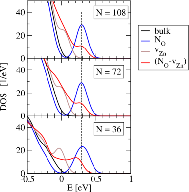
In order to check the influence of the finite supercell size on the defect levels obtained from our DOS calculations, we have compared calculations for three different supercell sizes, namely N=36, 72 and 108 atoms. As shown in Fig. 9, there is only very little change in level position and peak shape, when comparing the results for 72 and 108 atom supercells. On the other hand, the 36-atom supercells do not yet yield fully converged results, although the general conclusions could qualitatively also be drawn from these rather small cells. We therefore decided to use the 72-atom supercells for the results presented in the main part of the paper.
References
- (1) E.-C. Lee, Y.-S. Kim, Y.-G. Jin and K. J. Chang, Phys. Rev. B 64, 085120 (2001).
- (2) E.-C. Lee and K. J. Chang, Phys. Rev. B 70, 115210 (2004).
- (3) W.-J. Lee, J. Kang and K. J. Chang, Phys. Rev. B 73, 024117 (2006).
- (4) C. H. Park, S. B. Zhang and S. H. Wei, Phys. Rev. B 66, 073202 (2002).
- (5) S. Limpijumnong, S. B. Zhang, S.-H. Wei and C. H. Park, Phys. Rev. Lett. 92, 155504 (2004).
- (6) Y. Yan and S.-H. Wei, Phys. Stat. Sol. 245, 641 (2008).
- (7) L. G. Wang and A. Zunger, Phys. Rev. Lett. 90, 256401 (2003).
- (8) Y. Yan, J. Li, S. H. Wei and M. M. Al-Jassim, Phys. Rev. Lett. 98, 135506 (2007).
- (9) C. Y. Zhang, X. M. Li, X. D. Gao, J.L. Zhao, K. S. and J. M. Bian, Chem. Phys. Lett. 420, 448 (2006).
- (10) J. L. Lyons, A. Janotti and C. G. Van de Walle, Appl. Phys. Lett. 95, 252105 (2009).
- (11) S. Lany and A. Zunger, Phys. Rev. B 81, 205209 (2010).
- (12) W. Körner and C. Elsässer, Phys. Rev. B 81, 085324 (2010).
- (13) J. G. Reynolds, C. L. Reynolds Jr., A. Mohanta, J. F. Muth, J. E. Rowe, H. O. Everitt and D. E. Aspnes, Appl. Phys. Lett. 102, 152114 (2013).
- (14) L. Liu, J. Xu, D. Wang, M. Jiang, S. Wang, B. Li, Z. Zhang, D. Zhao, C.-X. Shan, B. Yao and D. Z. Shen, Phys. Rev. Lett. 108, 215501 (2012).
- (15) M. N. Amini, R. Saniz, D. Lamoen and B. Partoens, Phys. Chem. Chem. Phys. 17, 5485 (2015).
- (16) B. Wang, J. Min, Y. Zhao,W. Sang and C. Wang, Appl. Phys. Lett. 94, 192101 (2009).
- (17) A. Hierro, G. Tabares, J. M. Ulloa, E. Muñoz, A. Nakamura, T. Hayashi and J. Temmyo, Appl. Phys. Lett. 94, 232101 (2009).
- (18) W. Körner and C. Elsässer, Phys. Rev. B 83, 205315 (2011).
- (19) W. Körner, D. F. Urban, D. M. Ramo, P. D. Bristowe and C. Elsässer, Phys. Rev. B 90, 195142 (2014).
- (20) S. Sallis, K. T. Butler, N. F. Quackenbush, D. S. Williams, M. Junda, D. A. Fischer, J. C. Woicik, N. J. Podraza, B. E. White, Jr., A. Walsh and L. F. J. Piper, Appl. Phys. Lett. 104, 232108 (2014).
- (21) S. Sallis, N. F. Quackenbush, D. S. Williams, M. Senger, J. C. Woicik, B. E. White and L. F. J. Piper, Phys. Stat. Sol. (a) 212, 1471 (2015).
- (22) W. Körner, D. F. Urban and C. Elsässer, J. Appl. Phys. 114, 163704 (2013).
- (23) W. Körner, D. F. Urban and C. Elsässer, Phys. Stat. Sol. (a) 212, 1476 (2015).
- (24) A. Kurtz, A. Hierro, E. Muñoz, S. K. Mohanta, A. Nakamura, and J. Temmyo, Appl. Phys. Lett. 104, 081105 (2014).
- (25) P. E. Blöchl, Phys. Rev. B 50, 17953 (1994).
- (26) G. Kresse and J. Furthmüller, Phys. Rev. B 54, 11169 (1996).
- (27) G. Kresse and D. Joubert, Phys. Rev. B 59, 1758 (1999).
- (28) J. H. Rose, J. Ferrante and J. R. Smith, Phys. Rev. Lett. 47, 675 (1981).
- (29) C. Elsässer, N. Takeuchi, K. M. Ho, C. T. Chan P. Braun and M. Fähnle, J. Phys.: Condens. Matter 2, 4371 (1990).
- (30) K. M. Ho, C. Elsässer, C. T. Chan and M. Fähnle, J. Phys.: Condens. Matter 4, 5189 (1992).
- (31) B. Meyer, K: Hummler, C. Elsässer and M. Fähnle, J. Phys.: Condens. Matter 7, 9201 (1995).
- (32) F. Lechermann, M. Fähnle, B. Meyer and C. Elsässer, Phys. Rev. B 69, 165116 (2004).
- (33) W. Körner, P. D. Bristowe and C. Elsässer, Phys. Rev. B 84, 045305 (2011).
- (34) W. Körner and C. Elsässer, Phys. Rev. B 83, 205306 (2011).
- (35) J. P. Perdew and A. Zunger, Phys. Rev. B 23, 5048 (1981).
- (36) D. Vanderbilt, Phys. Rev. B 32, 8412 (1985).
- (37) D. Vogel, P. Krüger and J. Pollmann, Phys. Rev. B 54, 5495 (1996).
- (38) H. Ryoken, N. Ohashi, I. Sakaguchi, Y. Adachi, S. Hishita and H. Haneda, J. Cryst. Growth 287, 134 (2006).
- (39) R. Ghosh and D. Basak, J. Appl. Phys. 101, 023507 (2007).
- (40) A. Kaushal and D. Kaur Solar Energy Materials & Solar Cells 93, 193 (2009).
- (41) H. Nishinaka1, Y. Kamada, N. Kameyama, and S. Fujita, Phys. Stat. Sol. (b) 247, 1460 (2010).
- (42) B. Laumer, F. Schuster, M. Stutzmann, A. Bergmaier, G. Dollinger, and M. Eickhoff J. Appl. Phys. 113, 233512 (2013).
- (43) C. Franz, M. Giar, M.Heinemann, M. Czerner, and C. Heiliger, MRS Proceedings 1494, 57 (2013).
- (44) E. Gür, G. Tabares, A. Arehart, J. M. Chauveau, A. Hierro, and S. A. Ringel, J. Appl. Phys. 112, 123709 (2012).
- (45) C. W. Teng, J. F. Muth, U. Ozgur, M. J. Bergmann, H. O. Everitt, A. K. Sharma, C. Jin, and J. Narayan, Appl. Phys. Lett. 76, 979 (2000).
- (46) W. I. Park, G.-C. Yi, and H. M. Yang, Appl. Phys. Lett. 79, 2022 (2001).
- (47) Semiconductors: Physics of Group 4 Elements and 3-5 Compounds, edited by K. H. Hellwege and O. Madelung, Landbolt-Börnstein, New Series, Group 3, Vol. 17, Pt. A (Springer, Berlin 1982); Semiconductors: Intrinsic Properties of Group 4 Elements and 3-5-7, and 1-7 Compounds, edited by O. Madelung, W. von der Osten, and U. Rössler, Landolt-Börnstein, New Series, Group 3, Vol 22, Pt. A (Springer, Berlin 1987).
- (48) Y. Q. Gai, B. Yao, Z. P. Wei, Y. F. Li, Y. M. Lu, D. Z. Shen, J. Y. Zhang, D. X. Zhao, X. W. Fan, Jingbo Li, and Jian-Bai Xia, Appl. Phys. Lett. 92, 062110 (2008).
- (49) P. Muret, D. Tainoff, C. Morhain and J. M Cauveau, Appl. Phys. Lett. 101, 122104 (2012).
- (50) Y. F. Li, B. Yao, Y. M. Lu, Z. P. Wei, Y. Q. Gai, C. J. Zheng, Z. Z. Zhang, B. H. Li, D. Z. Shen, X. W. Fan, and Z. K. Tang, Appl. Phys. Lett. 91, 232115 (2007).
- (51) M. X. Qiu, Z. Z. Ye, H. P. He, Y. Z. Zhang, X. Q. Gu, L. P. Zhu, and B. H. Zhao, Appl. Phys. Lett. 90, 182116 (2007).
- (52) M. A. Alim, S. Li, F. Liu and P. Cheng, Phys. Stat. Sol. (a) 203, 410 (2006).
- (53) S. J. Clark, J. Robertson, S. Lany, and A. Zunger, Phys. Rev. B 81, 115311 (2010).
- (54) A. Janotti and C. G. Van de Walle, Phys. Rev. B 76, 165202 (2007).
- (55) F. Oba, A. Togo, I. Tanaka, J. Paier, and G. Kresse, Phys. Rev. B 77, 245202 (2008).
- (56) S. Sakong, J. Gutjahr an P. Kratzer, J. Chem. Phys. 138, 234702 (2013).