Design of Optical Tunable CNOT (XOR) and XNOR Logic Gates Based on D-Photonic Crystal Cavity Using Electro-Optic Effect
Abstract
We have proposed optical tunable CNOT (XOR) and XNOR logic gates using two-dimensional photonic crystal () cavities. Where, air rods with square lattice array have been embedded in Ag-Polymer substrate with refractive index of . In this work, we have enhanced speed of logic gates by applying two input signals with a phase difference at the same wavelength for cavities. Where, we have adjusted the phases of input and control signals equal with and zero, respectively. The response time of the structure and quality factor of the cavities are in the range of femtosecond and , respectively. Then, we have used electro-optic property of the substrate material to change the cavities resonance wavelengths. By this means, we could design the logic gates and demonstrate a tunable range of for their operation wavelength. The quality factor and the response times of cavities remain constant in the tunable range of wavelength, approximately. The evaluated least ON to OFF logic-level contrast ratios for the XOR and XNOR logic gates are and , respectively. The bit rates of the proposed logic gates can reach up to higher than values. According to the high rapid response time with acceptable quality factor of the cavities, the proposed optical logic gates can be considered as appropriate candidates to be building blocks for applications such as optical integrated circuits and optical processors with an ultrahigh speed of data flow.
I Introduction
According to the reported works to date, in information processors and communication systems, employing ultra-fast and cheap components provide them with competitive ability in market challenges. As a candidate to achieve this goal, based all-optical devices (all optical logic gates) has led to significant increment in operating speed and consequently in the performance bandwidth of the systems. However, according to the recent reports, the response time of these logic gates (more of them) has been enhanced to picoseconds (ps) range Fushimi2014 ; Christina2012 ; Noshad2007 ; Liu2008 . Fushimi et al. designed scalable all-optical logic gates with the same wavelength of the input and output signals. They allowed a wavelength fluctuation, with fraction of the cavity resonant wavelength widths. Then, they investigated cavities coupling to the waveguide and the operation degradation of logic gates. Also, Fushimi investigated the scalability of the designed logic gates considering their input power stability and tolerable fabrication errors Fushimi2014 . Christina et al. proposed all optical AND, NAND, XNOR and NOR logic gates based on s using self-collimation effect in a hexagonal structure by creating line defect in the structure Christina2012 . Noshad et al. proposed AND, NOR and NOT all optical logic gates based on s. They changed operational wavelength of the structure by embedding Kerr nonlinear rods in the structure Noshad2007 . Liu et al. proposed an all optical half adder based on cross structure . They first designed AND and XOR logic gates and then used them to make a half adder. They first designed an AND gate in a nonlinear structure and an XOR gate in another nonlinear structure and then combined them to make a half adder. Furthermore, they calculated an optimal operation speed without considering response time of the Kerr nonlinear material in the temporal range Liu2008 .
Using semiconductor micro-ring resonators is another alternative approach for all optical logic functions realizing Isfahani2009 ; Lin2013 . Bai et al. proposed all optical NOT and NOR logic gates by using a ring resonator. In this work they controlled the input signals by applying an optical probe wave to the ring. Where, wavelength of the probe and input signals were the same. Their logic gates were based on s Bai2009 . To the best of our knowledge, in the most of reported works, silicon rods have been used in the air or silica substrates but in among them some researchers have used ring resonators to perform logic gate functions. As instance, Andalib et al. could propose a controllable compact logic gate by using nonlinear ring resonators based on s Andalib2008 . They could also propose all optical AND and NOR logic gates by their proposed nonlinear ring resonator Andalib20081 ; Andalib2009 . In spite of their claim, the proposed gates were big in size and consequently had low operational speed. Also, other alternative methods such as all optical logic gate designing by using ultra small heterojunction diodes have been reported Wang2013 . They analyzed all-passive on-chip optical AND and NAND logic gates made from a directional emitting cavity connecting two ultra small heterojunction diodes. Where, the analyzed logic gates were phase insensitive. However, proposed logic gates by Fu et al. were depend on phase of the input signals that created along the wave guides at the structure Fu2012 .
Liu et al. proposed ultra-fast all optical AND, NAND, OR and NOR logic gates by using cavities based on s, which operates with low input power and very low response times in around of femtosecond () liu2011 . In this work, they utilized air rods in the Ag-Polymer substrate. By using the nonlinear property of Ag-Polymer they shifted the cavities resonance wavelength and thereby could propose all optical logic gates. According to other studies, the structures made of Polyester based on s have ultra-fast response times () liu2009 ; liu2005 ; Hu2005 .
On the other hand, tunable components are attractive subjects in the field of the modern optical communication systems extension. Tunable electro optical devices based on and also structures have been proposed Liu2004 ; Liu20051 ; Liu20041 ; Liu20052 ; Liu2006 . The experimental proof of an electro-optical was investigated and found to be in agreement with numerical results Amet2010 . Although photonic crystals can be employed to achieve low group velocities at their band edges, this is limited to a very narrow range of wave vectors in one particular direction. Recently, two-dimensional arrays of coupled photonic crystal resonators have been a study focus which exhibit reduced group velocities over the entire range of wave vectors Altug2005 ; Moreolo2008 . It is well known that the electro-optic effect has an ultra low response time of the order of nanosecond. This property makes it highly desirable and opens up the possibilities for ultra fast tunable devices with low power. Yang et al. have investigated a novel-designed two-dimensional coupled photonic crystal resonator array () realized in slabs filled with nonlinear polymer, which can dynamically tune the slow light properties in a wide frequency range and realize optical devices that could store and release optical pulses to implement values optical digital processing in future high speed optical networks Yang2011 .
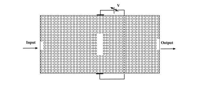
In the present work, we used s based cavities composed of air rods created in the Ag-polymer. It should be noted that we did not consider nonlinear properties of substrate (Ag-Polymer). The created phase shifts by the cavities was employed to propose all optical CNOT (XOR) and XNOR logic gates. This paper is composed of three sections. In the first section, we demonstrate and describe cavity, created in the 2DPhC, and the cavities resonance wavelengths with investigation of electro-optical effects of that on the cavities. In the second section, simulation results and their discussions have been presented and the final section is devoted to the conclusion and the obtained research results.
II Design and realization of structure
The employed cavity is created in a including air rods with radii perforated in the Ag-Polymer substrate with refractive index of and lattice constant of . By removing of some central air rods a L-type cavity is created, where removing of seven or eight rods from a single row of the results in or cavities, respectively. By decreasing radii of a line of nearest-neighbor rods of the cavity and also shifting them away, one can enhance the resonance wavelength () and quality factor () of the cavities. Here, we have decreased radii of a line of nearest-neighbor rods of the cavity to the value and also shifted them and the second neighbor rods away in about and , respectively. In table we show the values of and for the cavities. Also, the schematic structure of cavity is depicted in Figure .
| Cavity type | Resonate wavelength () | Quality factor () |
|---|---|---|
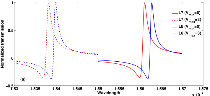
As indicated in table , the and values are different for each cavity type, which increase with increasing cavity type. For the cavity, the quality factor is equal to and for the is . Also according to table , the resonance wavelength of the and cavities are and , respectively.
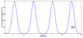
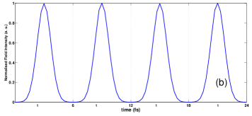
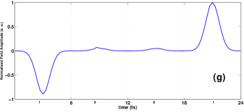
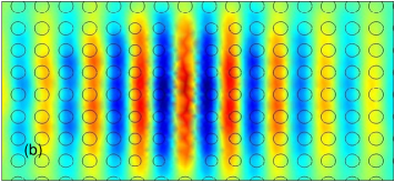
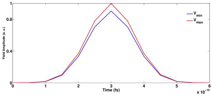
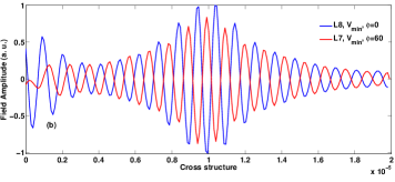
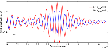
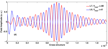
By applying a single mode optical field to the and cavities, we can demonstrate that cavities resonate with degrees phase difference. Normalized transmission spectrum profile for both of and cavity types are depicted in Figure . According to the Figure , it is observed that at wavelength , the transmitted electric field through cavity has a positive value while the transmitted electric field through cavity has a negative value. We employed this transmission characteristics of the cavities to propose ultra-fast all optical CNOT (XOR) and XNOR gates. The resonant optical fields within the and cavities experience a radian phase difference by applying a Gaussian pulse with central wavelength. The obtained phase difference cannot be retained through propagation in due to the material impaction. Then, the phase difference changes from radian to about ( ) at the output. To compensate this phase difference reduction, we applied the input signal of the cavity with a radian extra phase. According to the observed Gaussian output pulses, we can see that the proposed structure operate at very high speed () as illustrated in Figure . In Figure , one can observe that the resonance wavelengthes of cavities blue shift by increasing the applied voltage. Where, a wavelength tunable range from to has been achieved by the applied voltage increasing from to . Figure shows the optical intensity of signals with and without the extra phase through the structure. Figures and show evolution of the phase difference of cavities from to through the structure in the cases and , respectively, for without the extra phase case.
However, in the case of extra phase application (), Figures and illustrate the evolution of the optical fields amplitudes for the cavities through the structure in the cases and , respectively, as it is observed the phase difference evolution reach to in the output of structure. With comparing Figures and one can demonstrate that phase difference can be obtained in output, which is useful for realization of the claimed tunable optical logic gate.
III CNOT and XNOR logic gates
III.1 CNOT (XOR) gate
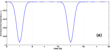
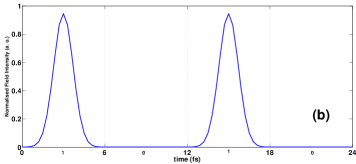
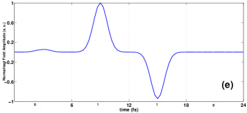
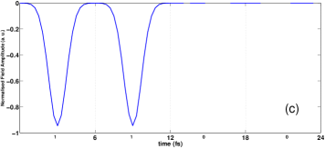
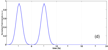
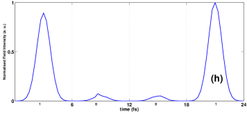
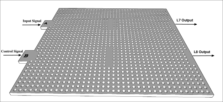
To design a CNOT optical logic gate, we used two and cavities in with square lattice of air rods. We applied an input signal to the cavity with phase of as input for the CNOT gate and another input signal applied to the cavity with input phase of as the control signal for the gate. Where, the field amplitude of control and input signals are equal. When the control field is set in zero logic level, with no signal applied to the cavity, the input signal of the cavity propagates to the output without any considerable reduction in its amplitude, as depicted in Figures within temporal range of to . However, when the control field is set in the high logic level, the reached pulse to the output of the gate is inverted of the input signal as depicted in Figures from to . Briefly, one can claim that no variation in the signal pulse amplitude is produced without applying any control signal. However, by applying a control signal, a radian phase difference is produced between the input and control signals, which results in a destructive interference at the output and disappearing of the output signal referred as the low logic level. As illustrated by Figure , the input of cavity is considered as the input port and the input of cavity as the control input of the CNOT gate. The central wavelength of the both input pulses was the same at . As explained in above, Figures exhibits the cavities responses with Gaussian input pulses application for performing all logical cases of the truth table for the CNOT logic gate. As an alternative view, one can consider the performance of the illustrated structure as an XOR gate, due to the wavelength and field amplitude sameness of the applied input and control signals. Here, the evaluated least ON to OFF logic-level contrast ratio for the XOR logic gate is calculated as .
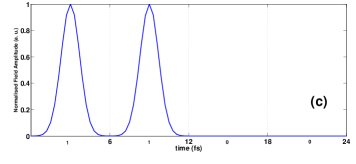
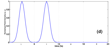
III.2 XNOR gate
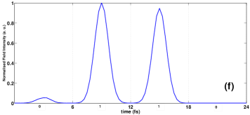
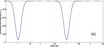
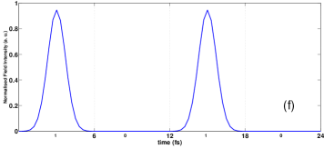
In order to realize an XNOR gate, we should utilize three input signals where each of them is applied for one of three cavities created in the . Here, there are two cavities to apply the input signals of the logic gate and one cavity for applying the control signal. For the XNOR gate, always, the control field is set in high logic level. When the input signals are set in low logic levels, without applying any input signal to any cavities, the applied control signal to the cavity propagates to the output without any considerable variation in its amplitude, as exhibited in Figures within temporal range of to . However, when any of the input signals is set in the high logic level, the received pulse to the output of the gate becomes zero, as depicted in Figures from to . As the last case, when both of the input signals are set in the high logic level, interference of them with the control field cause in emerging an output pulse in the high logic level as exhibited in Figures within the range of to . As the same as XOR, the evaluated least ON to OFF logic-level contrast ratio for the XNOR logic gate is obtained as . In this work, we have considered full width at half maximum () of the applied Gaussian signals equal with . Where, we have calculated the bit rate limit of for temporal performance of the simulated logic gates. Then the proposed gates could demonstrate acceptable response for the Gaussian input pulses with value of , temporally. Thus, it is reasonable that data flow in the proposed logic gates can be enhanced to ultrahigh rates of , approximately. In this section, we demonstrated the logic gates operation with minimum value of the applied voltage at the central wavelength of . According to the Figure we simulated operation of the gates at both extreme wavelengths of the achieved tunable range. Thus, the designed tunable logic gates based on the electro-optic property of the substrate material show suitable characteristics. Also, we would mention that one can design optical tunable logic gates with employing only or cavities by applying different voltages for each of the cavities.
IV Conclusion
The electro-optic property of the substrate material of the cavities is deployed in optical tunable CNOT (XOR) and XNOR gates functions achievement. Where, we applied Gaussian pulse signals at the central wavelength of as input signals for and cavities. Where, the resonance wavelength of the cavity can reduce from to by increasing the applied voltage to the each cavity. At any wavelength within the tunable range, a radian phase difference is produced between the cavities output signals. In summary, for retaining this phase difference at the output of the structure, as the logic gate output, we got need for an extra phase difference between input and control signals of the logic gate. Also, by temporal simulation of the designed logic gates, we demonstrated an ultra-fast logic operation and show their high potential as an appropriate candidate for applications such as tunable optical integrated circuits and optical processors.
References
- (1) Akihiro, F.; Takasumi T. Opt. Exp. 2014, 22, 4466-4479.
- (2) X. Susan Christina; A.P. Kabilan Pho. Sens. 2012, 2, 173-179.
- (3) Morteza, N.; Amin, A.; Reza, R.; Reza, Kh. Jour. of Phy. :Conf. series 2007, 350, 1-6.
- (4) Qiang, L.; Zhengbiao, O.; Chih, J.W.; Chung, P.L.; Jong, C.W. Opt. Exp. 2008, 16, 18992-19000.
- (5) Babak, M.I.; Tahereh, A.T.; Nosrat, G.; Ali, R.M.J. J. Opt. Soc. Am. B 2009, 26, 1097-1102.
- (6) Wen-Piao, L.; Yu-Fang, H.; Han-Lung, K. American Journal of Modern Physics 2013, 2, 144-147.
- (7) Jibo, B.; Junqin, W.; Junzhen, J.; Xiyao, C.; Hui, L.; Yishen, Q.; Zexuan, Q. Applied Optics 2009, 48, 6923-6927.
- (8) Parisa, A.; Nosrat, G. IEEE 2008, 170-172.
- (9) Parisa, A.; Nosrat, G.; J. Opt. Soc. Am. B 2008, 26, 10-16.
- (10) Parisa, A.; Nosrat, G. J. Opt. A: Pure Appl. Opt. 2009, 11, 11 1-7.
- (11) Chen, W.; Zhi-Yuan, L.The frontiers of phys. 2013, 103, 64001-64007.
- (12) Yulan, F.; Xiaoyong, H.; Qihuang, G. phys.Lett. A 2013, 377, 329-333
- (13) Ye, L.; Fei, Q.; Zi-Ming, M.;Fei, Z.; Qing-He, M.; Zhi-Yuan, Li. Opt. Exp. 2011, 19, 1945-1953.
- (14) Y. Liu, F. Qin, Z. Y. Wei, Q. B. Meng, D. Z. Zhang, Z.Y. Li, Appl. Phy. Lett. 2009, 95, 131116-131119.
- (15) Y. Liu, X. Hu, D. Zhang, B. Cheng, D. Zhang, Q. Meng, Appl. Phy. Lett. 2005, 86, 151102-151105.
- (16) X. Hu, Y. Liu, J. Tian, B. Cheng, D. Zhang, Appl. Phy. Lett. 2005, 86, 121102-121105.
- (17) C. Y. Liu, L. W. Chen, IEEE Photonics Technol. Lett. 2004, 16, 18491851.
- (18) C. Y. Liu, L. W. Chen, Opt. Commun. 2005, 256, 114-122.
- (19) C. Y. Liu, L. W. Chen, Opt. Express 2004, 12, 2616-2624.
- (20) C. Y. Liu, L. W. Chen , Phys. Rev. B: Condens. Matter Mater. Phys. 2005, 72, 045133-045138.
- (21) C. Y. Liu, L. W. Chen, Phys. E (Amsterdam, Neth.) 2006, 35, 173-177.
- (22) J. Amet, G. Ulliac, F. I. Baida, M. P. Berna, Appl. Phys. Lett. 2010, 96, 103111-103114.
- (23) H. Altug, H. Vuckovic, Appl. Phys. Lett. 2005, 86, 1-11.
- (24) M. S. Moreolo, V. Morra, G. Cincotti, Journal of Optics A: Pure and Applied Optics 2008, 10.
- (25) D. Yang; X. Wang, H. Tian, Y. Ji, Optica Applicata 2011, 41, 753.