Electronic transport of bilayer graphene with asymmetry line defects
Abstract
In this paper, we study the quantum properties of a bilayer graphene with (asymmetry) line defects. The localized states are found around the line defects. Thus, the line defects on one certain layer of the bilayer graphene can lead to an electric transport channel. By adding a bias potential along the direction of the line defects, we calculate the electric conductivity of bilayer graphene with line defects using Landauer-Büttiker theory, and show that the channel affects the electric conductivity remarkably by comparing the results with those in a perfect bilayer graphene. This one-dimensional line electric channel has the potential to be applied in the nanotechnology engineering.
I Introduction
Recently, graphene, a two-dimensional Dirac material1 ; 2 ; 3 ; 4 ; 5 ; 6 ; 7 becomes an attractive research field due to its exotic quantum properties, such as the unconventional quantum Hall effect, the Klein paradox 8 , the Josephson effect 9 , and the n-p junction 10 . Bilayer graphenes are weakly-coupled two single-layer graphene by interlayer carbon hopping, typically arranged in the Bernal (AB) stacking arrangement. In addition to the interesting underlying physics properties, bilayer graphenes have the potential electronics applications, owing to the possibility of controlling both the carrier density and energy band gap through doping or gating 11 ; 12 ; 13 ; 14 . A dual-gated structure allows electrical and independent control of the perpendicular electric field and the carrier density 15 ; 16 ; 17 . Intrinsic bilayer graphene has no band gap between its conduction and valence bands and the low-energy dispersion is quadratic with massless chiral quasiparticles18 ; 19 ; 20 . This is in contrast to what is observed in the monolayer which has a linear dispersion with massless quasiparticles.
In this paper, we consider a bilayer graphene with asymmetry line defects and study the defect states and the electric conductivity using the Landauer-Büttiker theory. This nontrivial physics properties of the defect states may be applied to a new type of devices based on the bilayer graphene.
The paper is organized as follows: Firstly, we introduce the tight-binding Hamiltonian of the bilayer graphene. Secondly, we calculate the energy structure of bilayer graphene with line lattice defects. Next, we show the effects of the line defects on the electric conductance, including the effects of defect-line number and the vertical electric field. Finally, summary and conclusions are provided.
II The tight-binding Hamiltonian
Bilayer graphene can be classified according to the stacking type. Generally, we focus on AB stacking, with an arrangement that was experimentally verified in epitaxial graphene by Ohta et al 21 .
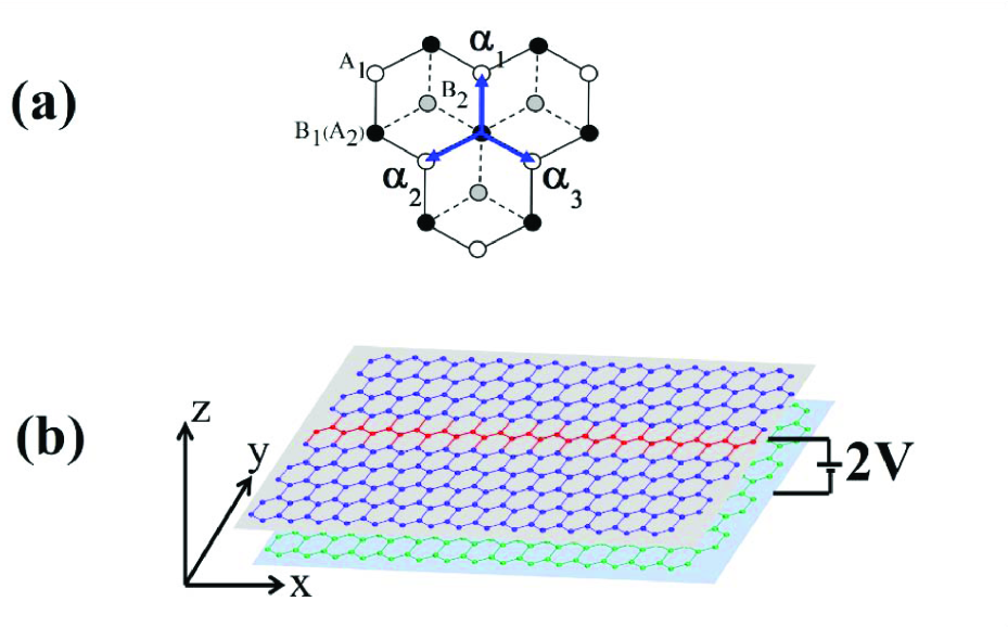
Fig.1(a) is an illustration of a bilayer graphene, that consists of four sublattices and the lattice constant is set to unit. To study the system simply, we mainly focus on the non-interaction case, of which an AB-stacked bilayer graphene model only contains first nearest-neighbor (NN) intralayer hopping and NN interlayer hopping. The tight-binding Hamiltonian is given by
| (1) |
Here, is the annihilation operator at sublattice at site where represents the upper layer and represents the lower layer of the bilayer material. The first term in the Hamiltonian describes intralayer nearest-neighbor coupling inside the layer, the second term describes the interlayer coupling between the sublattice of the lower layer and the sublattice of the upper layer and here we set eV, eV) 19.1 .
Due to spacial translation symmetry, intrinsic bilayer graphene can be described in momentum space and the number of sites in a primitive cell is four. Owing to the inversion symmetry in neutral bilayer graphene, there exists the degeneracy of the highest valence and lowest conduction bands. If the inversion symmetry is broken, an mass gap opens in the low energy spectrum 22 ; 23 ; 24 . When we assume that the upper and lower layers are at different electrostatic potentials (normally called bias potentials), the inversion symmetry is broken. Hence, the energy difference between the two layers is parameterized by the energy . Then, the Hamiltonian becomes
| (2) |
where is the external electrostatic potential. Here, we consider a staggered energy potential for bilayer graphene with on the upper layer and on the lower layer, where is a controllable constant quantity.
III Localized states induced by line defects
In this paper, we assume that a line-lattice defect lies on the upper layer, as represented by the highlighted red line marked in Fig.1(b), which is a zigzag lattice chain. To study the line defects on bilayer graphene, we simulate lattice defects on bilayer graphene by the following method: for a target lattice site on line defects, we set all the coupling hopping parameters connected to the site to and the local on-site energy potential to be a relatively larger value. To study the energy spectrum we assume the bilayer graphene is semi-infinite, that is, the system is finite along the -direction and infinite along the -direction. Thus, the line defect is an infinite zigzag chain along the -direction. To study the localized states induced by line defects, we use
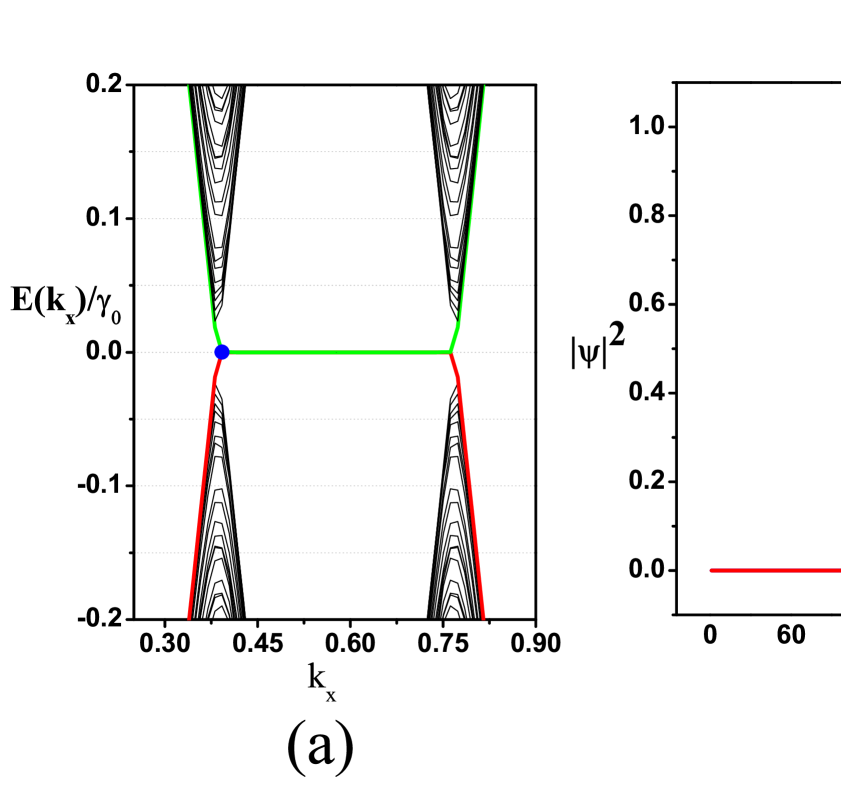
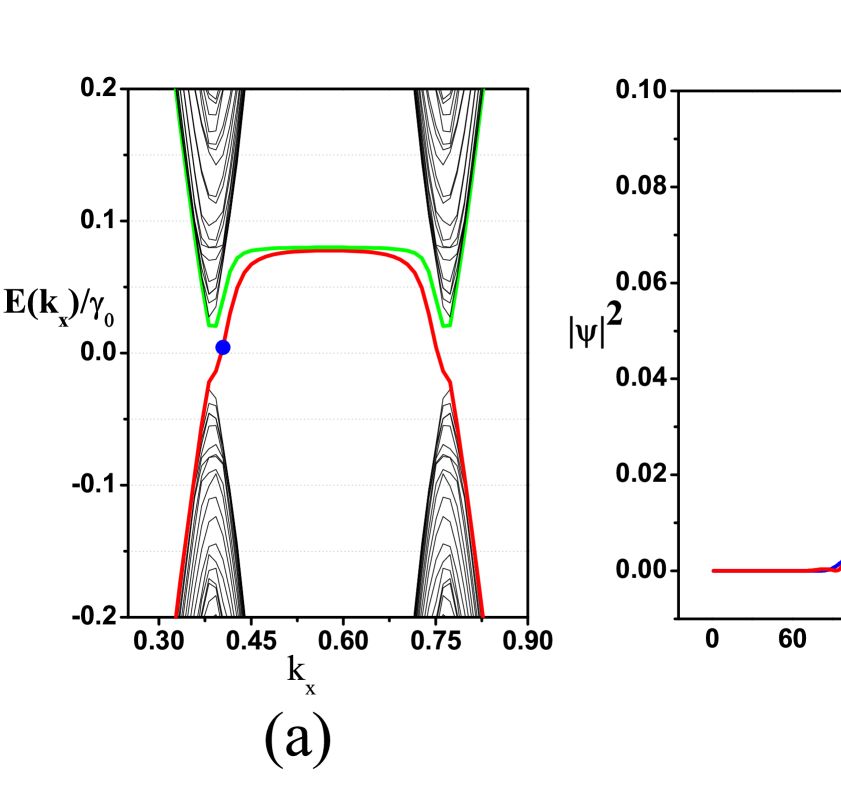
the period boundary conditions (PBC) along the -direction which makes the system a nanotube. By performing Fourier analysis and diagonalization, we may obtain the eigenvalues (or energy spectrum) and the corresponding eigenstates. The effects of the line defects and vertical electric potential are shown in Fig.2, Fig.3, Fig.4, respectively. For the case of , there exists bulk energy gap, and the value of the gap becomes larger with an increase of . In particular, a line defect leads to localized states (or defect states).
We consider a line defect on the upper layer and set the total number of zigzag chain (parallel to the red zigzag line in Fig.1(b)) along -direction to be . When there exist defect states (marked by the red solid line and green solid line in Fig.2(a)) and zero-energy states, which has a flat band. For this case, the wave function of zero-energy state is localized around the defects (Fig.2(b)). The length-scale of the localized states along -direction is where is the energy gap of bulk system. For the case of , we also have the localized states around line defects. For this case, a bulk gap appears and the defect states becomes dispersive. The probability density of zero-energy wave function becomes extended on both upper layer and lower layer of the bilayer graphene, and the maximum value of is on the corresponding positions on lower layer.
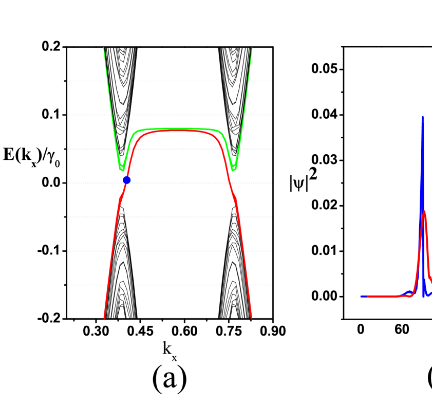
Furthermore, we can also study the cases with several parallel line defects. For two parallel line defects on the upper layer, there exists localized defect states which are located around corresponding line defects, and the electric field induces a finite bulk energy gap (Fig.4).
IV Transport properties of a bilayer graphene with asymmetry line defects
Bilayer graphene exhibits nontrivial transport properties owing to its unusual band structure where the conduction and valence bands touch with quadratic dispersion. One of the earliest theoretical papers studying the conductivity through AB-stacked bilayer graphene was Ref. 25 where it was assumed that the band structure of the bilayer is described by two bands closest to the Dirac point energy. Transport properties and the nature of conductivity near the Dirac point were probed experimentally 1 ; 26 and investigated theoretically 27 .
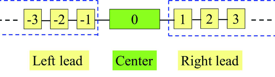
We use the well-known Landauer-Büttiker equation to obtain the electric conductivity. To show the effect of the line defect on the electric conductance, we seperate the original system into three parts: left lead, right lead and the center device area, as shown in the schematic diagram in Fig.5. The left and right leads are semi-infinite and the center device area has finite size. The number of primitive cells along the -direction is ; the number of zigzag chain along the -direction is . Here, it is a zigzag edge along the -direction and an armchair edge along the -direction. Hence, for the lead-center-lead bilayer graphene system, the zero-temperature conductance is calculated using the Landauer-Büttiker formalism 28 :
| (3) |
where is the transmission from the incoming state in the left lead to the outgoing state in the right lead. The terminal electric conductance can be written as and the transmission probability through it is
| (4) |
where is the left (right) coupling matrix, and is the retarded (advanced) Green’s function of the center part of the system.
The single particle Green’s function of the center devise area is defined as
| (5) |
where is the energy of the particle, is a positive infinitely-small real number, represents the identity matrix, and is the Hamiltonian of the center devise area. () are the contact self-energies reflecting the effect of coupling of the center part of the graphene to the left (right) leads. We obtain the expressions for the self-energies of the two leads as
| (6) |
where is the coupling matrix of the center part to the right (left) lead. Subsequently, we can successfully calculate the electron transmission probability using . are the surface Green’s functions of the right (left) leads. Hence, we can determine the conductivity in the presence and absence of line defects.
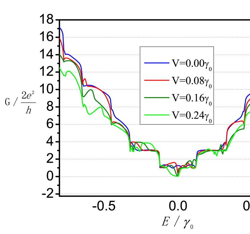
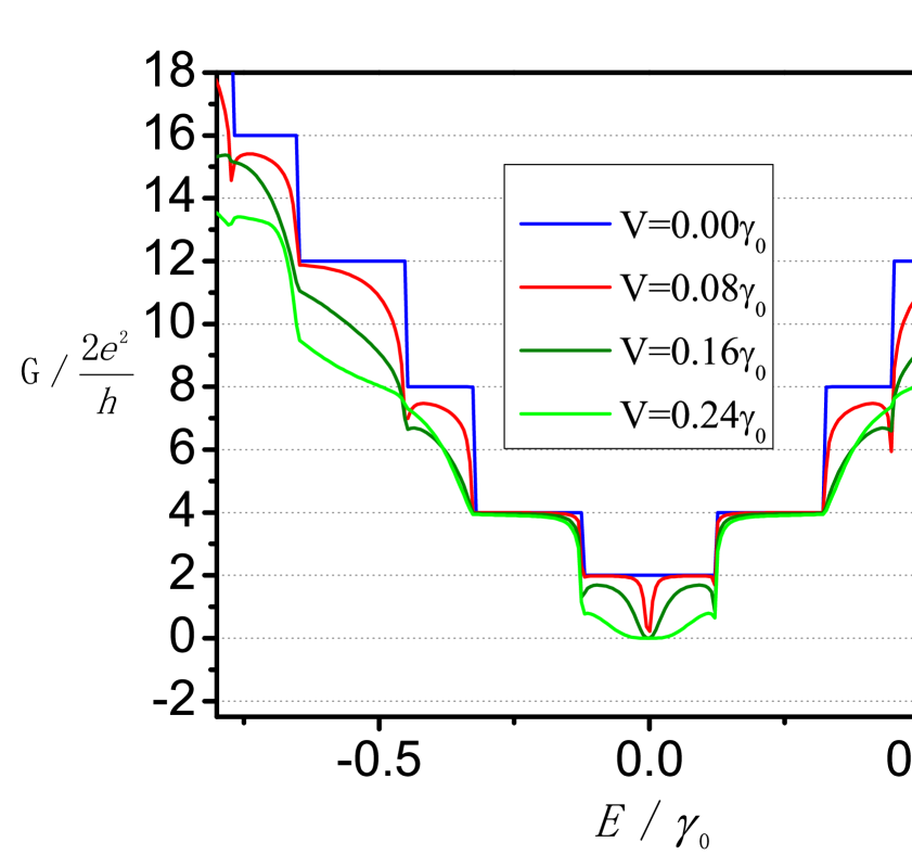
To compare with the electrical transport effects of the line defects, the electric conductance of perfect bilayer graphene devices is also given (Fig.6). We use PBC along the -direction, that is, the center devices area is a bilayer graphene nanotube. When , the value of near is , which is double to the value of one layer graphene owing to the degeneracy of the highest valence and lowest conduction bands. When , the value of at approaches zero, which indicates that the system generates a bulk energy gap, and the larger results in a larger width of gap. However, the electric conductance shows additional features induced by the line defects as shown in Fig.7. When the value of near is about . When there is , and from the contrast of pure bilayer graphene and symmetric defects it is clear that this is the result of the particle-hole symmetry breaking by the asymmetric defects 29 ; 30 . Now, the degeneracy of the zero energy is left and the energy spectrum becomes asymmetry. Hence, the conductance can be controlled by the vertical electric potential and the line defects in this case. As a result, this one-dimensional line electric channel has the potential to be applied in the nanotechnology engineering.
V Conclusion
In this paper, we studied the physics properties of a bilayer graphene with line defects, including the defect-induced localized states and the electric conductivity. We found that the line defect on a certain layer of the bilayer graphene leads to an electric channel. When , the localized states on single layer has a flat band with zero energy. When the system becomes gapped and the localized modes have the distribution on both layers. The additional conductance from line defect is obtained. This effect from line defects may be applid in electronic devices based on bilayer graphene.
Acknowledgements.
This work is supported by National Basic Research Program of China (973Program) under the grant No. 2011CB921803, 2012CB921704 and NSFC GrantNo.11174035, 11474025, 11504285, 11404090 and SRFDP, the Fundamental Research Funds for the Central Universities, and the Scientific Research Program Funded by Shanxi Provincial Education Department under the grant No. 15JK1363.References
- (1) Novoselov K. S., Geim A. K., Morozov S. V., Jiang D., Katsnelson M. I., Grigorieva I. V., Dubonos S. V., and Firsov A. A., Nature 438,197 (2005)
- (2) Zhang Y., Tan Y.-W., Stormer H. L., and Kim P., Nature London 438, 201 (2005)
- (3) Xu, X., Yao, W., Xiao, D. Heinz, T. F., Nature Phys.10, 343 (2014)
- (4) Xiao, D., Yao, W. Niu, Q., Phys. Rev. Lett. 99, 236809 (2007)
- (5) Mak K. F., McGill K. L., Park J. McEuen P. L., Science 344, 1489 (2014)
- (6) Gorbachev R. V. et al. Science 346, 448 (2014)
- (7) Novoselov K. S., Geim A. K., Morozov S. V., Jiang D., Zhang Y., Dubonos S. V., Grigorieva I. V., and Firsov A. A., Science 306, 666 (2004)
- (8) Katsnelson M. I., Novoselov K. S., and Geim A. K., Nat. Phys. 2, 620 (2006)
- (9) Titov M. and Beenakker C. W. J., Phys. Rev. B 74, 041401(R) (2006)
- (10) Cheianov V. V. and Fal’ko V. I., Phys. Rev. B 74, 041403(R) (2006)
- (11) McCann E and Fal’ko V. I., Phys. Rev. Lett. 96, 086805 (2006)
- (12) Guinea F., Castro Neto A. H. and Peres N. M. R., Phys. Rev. B 73, 245426 (2006)
- (13) Ohta T., Bostwick A., Seyller T., Horn K. and Rotenberg E., Science 313, 951 (2006)
- (14) Castro E. V., Novoselov K. S., Morozov S. V., Peres N. M. R., Lopes dos Santos J. M. B., Nilsson J., Guinea F., Geim A. K. and Castro Neto A. H., Phys. Rev. Lett. 99, 216802 (2007)
- (15) Oostinga J. B., Heersche H. B., Liu X., Morpurgo A. F. Vandersypen L. M. K., Nature Mater. 7, 151 (2007)
- (16) Zhang Y. et al. Nature 459, 820 (2009)
- (17) Taychatanapat T. Jarillo-Herrero P., Phys. Rev. Lett. 105, 166601 (2010)
- (18) Zhang Y., Tang T.-T., Girit C., Hao Z., Martin M. C., Zettl A., Crommie M. F. , Shen Y. R., and Wang F., Nature 459, 820 (2009)
- (19) Sui M.Q., Chen G.R., Ma L.G., Shan W.Y., Tian D., Watanabe K., Taniguchi T., Jin X.F., Yao W., Xiao D., Zhang Y.B., Nature Physics 11, 1027(2015)
- (20) Dresselhaus M S, Dresselhaus G, Advances in physics, 51(1),1 (2002).
- (21) Shimazaki Y., Yamamoto M., Borzenets I. V., Watanabe K. , Taniguchi T. and Tarucha S., Nature Physics 11, 981 (2015)
- (22) Ohta T., Bostwick A., McChesney J. L., Seyller T., Horn K. , and Rotenberg E., Phys. Rev. Lett. 98, 206802 (2007)
- (23) McCann E. and Falko V.I., Phys. Rev. Lett. 96, 086805 (2006)
- (24) McCann E., Phys. Rev. B 74, 161403(R) (2006)
- (25) Bostwick A., T. Ohta, J.L. McChesney, K.V. Emtsev, T. Seyller, K. Horn, and E. Rotenberg, New J. Phys. 9, 385 (2007)
- (26) Koshino M. and Ando T., Phys. Rev. B 73, 245403 (2006)
- (27) Zhang Y. B., Tan Y. W., Stormer H. L. and Kim P., Nature 438, 201 (2005)
- (28) Koshino M. and Ando T., Phys. Rev. B 73, 245403 (2006)
- (29) Paramita Dutta, Santanu K. Maiti and Karmakar S. N., Journal of Applied Physics 114, 034306 (2013)
- (30) Rhim J W, Moon K. Journal of Physics: Condensed Matter, 20.36, 365202 (2008).
- (31) Eduardo V. Castro, N. M. R. Peres, J. M. B. Lopes dos Santos, A. H. Castro Neto, and F. Guinea, Phys. Rev. Lett. 100, 026802 (2008)