Topological Phases in InAs1-xSbx:
From Novel Topological Semimetal to Majorana Wire
Abstract
Superconductor proximitized one-dimensional semiconductor nanowires with strong spin-orbit interaction (SOI) are at this time the most promising candidates for the realization of topological quantum information processing. In current experiments the SOI originates predominantly from extrinsic fields, induced by finite size effects and applied gate voltages. The dependence of the topological transition in these devices on microscopic details makes scaling to a large number of devices difficult unless a material with dominant intrinsic bulk SOI is used. Here we show that wires made of certain ordered alloys InAs1-xSbx have spin splittings up to 20 times larger than those reached in pristine InSb wires. In particular, we show this for a stable ordered CuPt-structure at , which has an inverted band ordering and realizes a novel type of a topological semimetal with triple degeneracy points in the bulk spectrum that produce topological surface Fermi arcs. Experimentally achievable strains can drive this compound either into a topological insulator phase, or restore the normal band ordering making the CuPt-ordered InAs0.5Sb0.5 a semiconductor with a large intrinsic linear in bulk spin splitting.
In recent years, a range of topological phases have been realized in materials, ranging from topological insulators Hasan and Kane (2010); Qi and Zhang (2011) (TIs) and semimetals Turner and Vishwanath (2013); Wan et al. (2011); Wang et al. (2013a); Liu et al. (2014) (TSMs) to superconductors Volovik (2009); Leijnse and Flensberg (2012) (TSCs). The non-trivial topology of the ground state wavefunctions in these phases causes a variety of phenomena in such materials ranging from topologically protected metallic surface or edge states in TIs Hasan and Kane (2010); Qi and Zhang (2011) and Fermi arcs and anomalous magnetotransport in TSMs Nielsen and Ninomiya (1981); Wan et al. (2011); Hosur and Qi (2013); Son and Spivak (2013), to quasiparticles with non-Abelian particle statistics Ivanov (2001); Read and Green (2000); Nadj-Perge et al. (2014); Lutchyn et al. (2010); Oreg et al. (2010); Alicea (2010, 2012); Mourik et al. (2012) in TSCs, which could be used for topological quantum computation Kitaev (2003); Nayak et al. (2008).
Arguably the simplest scheme for realizing non-Abelian statistics in a solid-state device is based on manipulating Majorana zero modes (MZMs) in networks of semiconductor wires. MZMs were predicted to appear at the ends of spin-orbit coupled wires subject to a parallel magnetic field, proximity coupled to an -wave superconductor. Experimental observations, consistent with the theory, were reported for InAs and InSb zincblende nanowires Das et al. (2012); Deng et al. (2012); Mourik et al. (2012); Albrecht et al. (2016).
The stability of MZMs in such a setup depends greatly on the size of the spin-orbit splitting (SOS) of the conduction band. SOS is very small in bulk zincblende semiconductors Dresselhaus (1955) and the realization of the MZMs thus relies on the externally induced Rashba SOS Bychkov and Rashba (1984), which is estimated to be of the order of 1 meV van Weperen et al. (2015); Soluyanov et al. (2016). This value is very small compared to the bulk splitting in some recently discovered compounds (Bahramy et al., 2011; Picozzi, 2014; Zhu et al., 2013; Eremeev et al., 2012). However, most of these materials are not suitable for realizing MZMs within the above scenario, while for others such experiments appear to be challenging. It is thus desirable to understand if large values of bulk SOS can be achieved within the III-V materials class, used in most experiments at this time. A bulk SOS dominating the Rashba contributions would also make realization of MZMs far less sensitive to particular microscopic details of a specific device.
In this Letter we argue that certain ordered alloys with composition InAs1-xSbx have sizable SOS and provide an optimal material for the realization of MZMs. For ternary alloys to give an advantage over fixed binary III-V compounds, SOS should be enhanced, ideally while preserving the high carrier mobility. We thus focus our attention on ordered superlattice structures. We find, in particuar, that a CuPt-ordering with is energetically stable and hosts a novel TSM phase, which is identified as an interpolation of the established Dirac Wang et al. (2012); Yang and Nagaosa (2014); Wang et al. (2013b) and Weyl Wan et al. (2011); Volovik (2009) TSMs. Moreover, the TSM phase can be tuned either into a TI or normal insulator phase by application of strain. We also find that for the latter the spin-orbit energy 111The definition of is given in Fig. 6(a) can be as large as 24 meV. Experimental evidence for the CuPt-ordering of InAs0.5Sb0.5 exists Jen et al. (1989); Stringfellow and Chen (1991); Kurtz et al. (1992); Ercolani et al. (2012); Belenky et al. (2015), and we argue that nanowires of this structure can be grown with molecular beam epitaxy.
The SOS of the conduction band in zincblende structures is at most cubic in around the -point Dresselhaus (1955). In both III-V materials, the conduction band has a minimum at and an -like character dictated by symmetry. A SOS linear in can thus only be achieved by breaking the symmetry. We ask the question if there is a modification to the III-V materials, such that a bulk linear in SOS is achieved.
Disorder in nanoscale structures
— In the randomly disordered alloy InAs1-xSbx any symmetry breaking terms need to vanish because of averaging. However, in a nanoscale device, like a quantum dot or wire, the averaging will not be complete and a “bulk” contribution to the linear in SOS is expected. We study this effect by simulating randomly disordered cubic supercells of InAs1-xSbx 222The virtual crystal approximation Bellaiche and Vanderbilt (2000) (VCA), which is a standard approximation for simulating alloying, is not able to reproduce experimentally known features of InAs1-xSbx, such as the nonlinear bowing of the fundamental energy gap and the spin-orbit gap (see Fig. 1(a)) Chadi (1977); Cripps et al. (2008); Svensson et al. (2012).. The supercell calculations are faciliated within Slater-Koster tight-binding models Slater and Koster (1954) of the sp3s∗ type Vogl et al. (1983); Klimeck et al. (2000); Carlo (2003), with parameters derived from first principles bulk calculations employing the HSE06 hybrid functional Heyd et al. (2003); Heyd and Scuseria (2004); Heyd et al. (2006); Kim et al. (2009). See Supplementary Material 333See Supplementary Information for a detailed description of (additional) first principles calculations, tight-binding models, derivation of models, details on the topological classification and Landé -factor calculation. for technical details on the calculation.
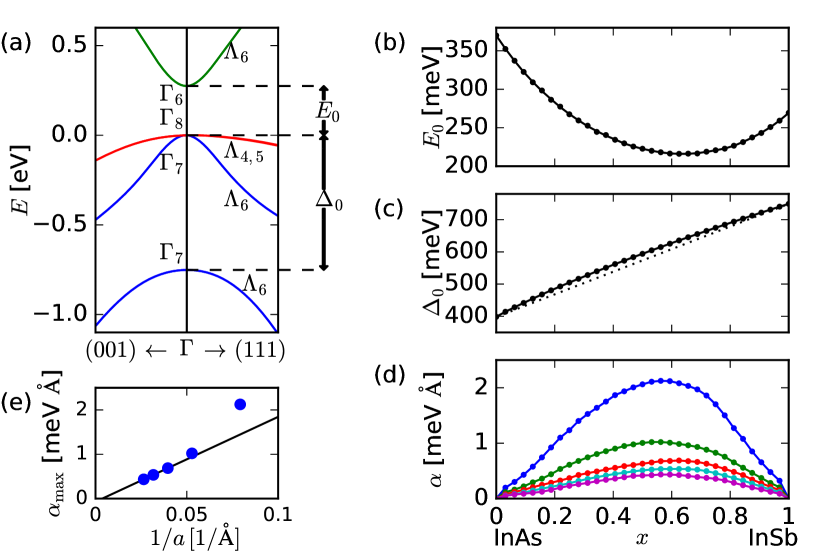
Figure 1 (b-c) show the composition dependence of the band gap and the spin-orbit gap . The curves and exhibit the correct bowing (non-linearity), and are in good agreement with recent experiments Cripps et al. (2008); Svensson et al. (2012); Suchalkin et al. (2016). The linear in SOS of the lowest conduction band is quantified by fitting the band structure calculations to an effective Hamiltonian
| (1) |
The parameter plays the role of the Rashba parameter in standard models for Majorana wires Alicea (2012); Lutchyn et al. (2010); Oreg et al. (2010). The magnitude of this coefficient varies with the -space direction, and its dependence on disorder realizations is shown in Fig. 1(d) for the (110) direction 444Which is the direction of the maximal SOS in pure zincblende semiconductors for small Winkler (2003); Luo et al. (2009); Soluyanov et al. (2016).. As expected, decreases due to averaging when the supercell size is enlarged, which is also shown in Figure 1(e). As a consequence, wires or quantum dots of randomly alloyed InAs1-xSbx have a universal bulk contribution to the SOS that depends strongly on the size of the device.
CuPt-ordered structure
— In contrast to the disordered configurations above, symmetry breaking by alloy ordering is nonvanishing for arbitrary system size. Since Fig. 1(d) shows that is maximized in the vicinity of we focus on small ordered supercells with as good candidates for realization of large SOS, maximizing . In particular, we considered three types of ordering reported in experiments on III-V ternary alloys Stringfellow and Chen (1991): ordering in {100} planes (CuAu-I or L10 structure), ordering in {210} planes (chalcopyrite or E11 structure) and ordering in {111} planes (CuPt or L11 structure). The CuPt-type ordering is energetically stable in InAs0.5Sb0.5 Note (3) and has been experimentally observed under various growth conditions Jen et al. (1989); Stringfellow and Chen (1991); Kurtz et al. (1992); Ercolani et al. (2012); Belenky et al. (2015). We find that this structure also has the biggest enhancement of the SOS (see Supplementary Material Note (3)). We thus consider this type of ordering in the following.
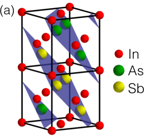
In the CuPt-ordered InAs0.5Sb0.5 structure, shown in Fig. 2(a), atoms of As and Sb are arranged in {111} planes that grow in the alternating order In-As-In-Sb. This ordering reduces the (space group #216) symmetry of the pristine zincblende compounds to (space group #160), that has a three-fold rotational axis coinciding with the (111) direction, and three vertical mirror planes that contain the symmetry axis and are rotated by relative to each other. Both the ionic positions and lattice vectors were relaxed using the HSE06 hybrid functional to get the lowest energy structure. We found the deviation from the cubic structure to be smaller than 0.1% Note (3).
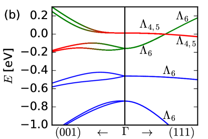
The band structure of CuPt-ordered InAs0.5Sb0.5 obtained with HSE06 is shown in Fig. 2(b). The little group of -points on the (111)-axis in the CuPt-structure is as in the zincblende structure, hence the same symmetry label is used for the bands in Figs. 1(a) and 2(b). While the bands have a very small, linear in , splitting, the bands of the representation are doubly degenerate. Note that the ordering of the valence and conduction bands at is interchanged for the two structures, resulting in a band inversion in the CuPt-structure. We find the band inversion to be stable against deviations from the CuPt-order, in particular we find that CuPt-ordered InAs0.67Sb0.33 and InAs0.33Sb0.67 still show a strong band inversion Note (3).
A novel TSM
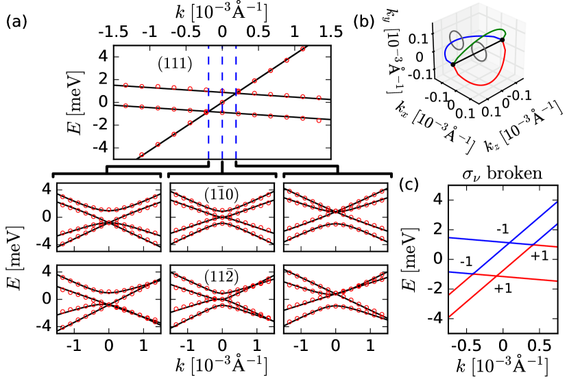
— In the inverted band structure the and bands cross (see Fig. 3(a)) to form a new type of a TSM. While theoretical evidence for the band inversion in ordered InAs0.5Sb0.5 was reported previously Wei and Zunger (1991), the topology of this semimetal phase was overlooked.
Here the crossings are protected by the -rotational symmetry. For inversion-symmetric materials is known to stabilize Dirac points on the high-symmetry axis Wang et al. (2012); Turner and Vishwanath (2013); Yang and Nagaosa (2014). The inversion symmetry is absent in InAs0.5Sb0.5, so that two of the four bands that would form a Dirac point are gapped. Along the (111)-axis, the two singly degenerate bands each cross with the doubly degenerate forming triply degenerate crossings, or triple points (TPs). In the other two directions each TP splits into two linearly dispersing bands and a quadratically dispersing one (see Fig. 3(a)). Previously, TPs have been discussed in the context of Bernal-stacked graphite with neglected SOI Mikitik and Sharlai (2008); Heikkilä and Volovik (2015); Hyart and Heikkilä (2016), spin-1 quasiparticles in two dimensions Bercioux et al. (2009); Green et al. (2010) and strained HgTe Zaheer et al. (2013). The TP we find is furthermore accompanied by four Weyl nodal lines Burkov et al. (2011) in the vertical mirror planes, degenerate lines between the second and third band in Fig. 3(a), each protected by a Berry phase of (see Fig. 3(b)).
| (meV) | (eV Å) | (eV Å) |
|---|---|---|
| 0.88 | -0.42 | 4.22 |
| (eV Å) | (eV Å) | (eV Å) |
| 0.78 | 2.14 |
In the vicinity of the crossing point the band structure can be described by the following model (see Supplementary Material Note (3))
| (2) |
For InAs0.5Sb0.5 the values of the parameters obtained from fits to the first-principles calculations are listed in Tab. 1, and the fit is shown in Fig. 3(a). The momentum here is given relative to the crossing point , and is taken to be in the (111)-direction and in the -direction.
While a detailed description and topological classification of this novel TSM phase will be provided elsewhere Zhu et al. (2016), we outline the proof of the topological origin of this phase here. An illustrative verification of the topological origin of this phase is obtained by breaking the mirror symmetry of the group. The doubly degenerate band splits into two bands, and four crossings are formed as shown in Fig. 3(c). All the four crossings represent Weyl points, with their chiral charges shown in the figure Note (3). On the other hand, if all inversion symmetry breaking terms are tuned to zero one obtains a Dirac TSM and thus the TP TSM can be seen as an interpolation of Dirac and Weyl TSMs.
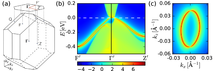
The presence of Dirac or Weyl points in the bulk spectrum of metals is associated with the appearance of Fermi arcs in the surface spectrum Weng et al. (2015); Soluyanov et al. (2015); Lv et al. (2015); Huang et al. (2015); Wang et al. (2012, 2013b); Xu et al. (2015). Fig. 4 shows the surface density of states, obtained by the iterative Green’s function method Sancho et al. (1985). Topological surface states forming the two Fermi arcs that connect the two pairs of TPs at opposite are clearly visible, similar to the ones found in Dirac TSMs. Furthermore, we show in the Supplementary Material Note (3) that the Landau level spectrum is gapless for a magnetic field aligned parallel to the symmetry axis, hinting at anomalous transport in the presence of magnetic fields Nielsen and Ninomiya (1981); Hosur and Qi (2013); Son and Spivak (2013).
Optimizing the structure for MZMs
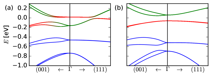
— Having established the existence of a novel TSM phase in InAs0.5Sb0.5, we now return to our original purpose of finding an optimal structure for MZM realization. Upon breaking the symmetry by strain (e.g. (001)-strain) the degeneracy at the TPs is lifted and the system becomes a semiconductor. The inverted band structure makes it a strong 3D TI in this case, as verified by computing the topological invariant Gresch et al. (2016). Figure 5 (a) shows the HSE06 band structure for 1% compressive strain in (001) direction, when all the symmetries of the structure are broken. In this configuration MZMs can appear in proximitized wires of TIs as discussed by several works Cook and Franz (2011); Cook et al. (2012).
The ordinary band ordering in CuPt-ordered InAs0.5Sb0.5 can be restored by applying a symmetry-preserving compressive (111)-strain of 2%. Such strain values are easily achievable in nanowires due to lattice mismatch Ercolani et al. (2009); Larsson et al. (2007). Moreover, epitaxial semi-super InAs/Al nanowires were reported to bend during the growth process, thus being naturally strained asymmetrically along the (111) growth direction Krogstrup et al. (2015).
| Material | ||||||
|---|---|---|---|---|---|---|
| [eV Å] | 0.0 | 0.8 | 1.0 | 1.1 | 1.0 | |
| [meV] | 0.0 | 2.7 | 3.4 | 3.5 | 3.5 | |
| InAs0.5Sb0.5 | [] | 0.24 | 0.16 | 0.14 | 0.12 | 0.13 |
| -2% (111)-strain | [Å] | 60 | 55 | 60 | 60 | |
| 115 | 95 | 65 | 194 | 177 | ||
| [] | 0.0 | 1.0 | 1.1 | 1.1 | 1.1 | |
| [eV Å] | 0.0 | 0.8 | 1.2 | 1.4 | 1.4 | |
| [meV] | 0.0 | 6 | 14 | 24 | 24 | |
| InAs0.5Sb0.5 | [] | 0.47 | 0.37 | 0.41 | 0.47 | 0.50 |
| -3% (111)-strain | [Å] | 25 | 16 | 11 | 11 | |
| 83 | 69 | 47 | 164 | 161 | ||
| [] | 0.0 | 1.5 | 1.7 | 1.7 | 1.8 |
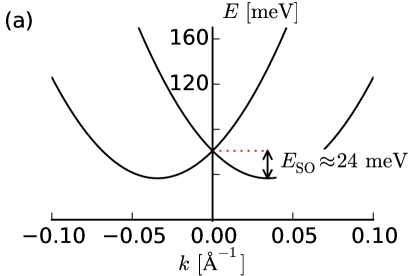
The HSE06 band structure of (111)-strained InAs0.5Sb0.5 is shown in Fig. 5(b) for a 3% strain. In this case the conduction bands acquire a sizable linear in SOS in any direction but (111) (see Tab. 2). We find that the Rashba coefficient is significantly larger than that reported for pristine InSb nanowires van Weperen et al. (2015), and the corresponding can reach values up to 24 meV, as illustrated in Fig. 6(a) and Tab. 2. Note, that the SOS considered here is bulk only and will additionally contribute to the Rashba splitting appearing in a confined geometry.
From Tab. 2 one can see that is large for all the directions orthogonal to the -axis. Thus, an optimal SOS is achieved in wires grown in the plane of CuPt-structure atomic layers. This suggests gate-defined wires Reuther et al. (2013) in (111) thin films of InAs0.5Sb0.5 to be the most advantageous route to increased stability of MZMs. Additionally, the confinement of the quantum well in the (111) direction has a similar effect as strain and can restore the normal band order for thin quantum wells as is the case in HgTe quantum-wells Bernevig et al. (2006).
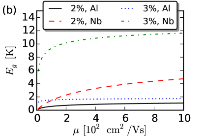
To give a rough estimate for the realistic value of a TSC gap induced in InAs0.5Sb0.5, we used the obtained parameters in the effective model analysis of Ref. Sau et al. (2012) to calculate the disorder renormalized quasiparticle gap in the TSC state. The gap values in the adjacent bulk superconductor are taken to be 2 K for Al and 15 K for Nb. In Fig. 6(b) is plotted as a function of the mobility , and Tab. 2 lists values of assuming Al as the bulk superconductor and a mobility of . Even with this moderate electron mobility is almost an order of magnitude larger in InAs0.5Sb0.5 than what is currently achievable in pure InSb van Weperen et al. (2015).
Finally, we considered other III-V alloys, for which CuPt-ordering was reported in Ref. Stringfellow and Chen (1991). We found that InP0.5Sb0.5 and GaAs0.5Sb0.5 realize the novel TSM phase reported above for InAs0.5Sb0.5. Of the compounds with normal band ordering Al0.5Ga0.5As and Al0.5In0.5Sb exhibit the largest values of , which is small compared to InAs0.5Sb0.5, being of order 0.1 meV Note (3).
Acknowledgments. We would like to thank C. M. Marcus, M. Wimmer and D. Gresch for useful discussions. G. W. W. wants to thank specifically T. Hyart for a correction and useful discussions. This work was supported by Microsoft Research, the European Research Council through ERC Advanced Grant SIMCOFE, and the Swiss National Science Foundation through the National Competence Centers in Research MARVEL and QSIT.
References
- Hasan and Kane (2010) M. Z. Hasan and C. L. Kane, Rev. Mod. Phys. 82, 3045 (2010).
- Qi and Zhang (2011) X.-L. Qi and S.-C. Zhang, Rev. Mod. Phys. 83, 1057 (2011).
- Turner and Vishwanath (2013) A. M. Turner and A. Vishwanath, ArXiv e-prints (2013), arXiv:1301.0330 [cond-mat.str-el] .
- Wan et al. (2011) X. Wan, A. M. Turner, A. Vishwanath, and S. Y. Savrasov, Phys. Rev. B 83, 205101 (2011).
- Wang et al. (2013a) Z. Wang, H. Weng, Q. Wu, X. Dai, and Z. Fang, Phys. Rev. B 88, 125427 (2013a).
- Liu et al. (2014) Z. K. Liu, J. Jiang, B. Zhou, Z. J. Wang, Y. Zhang, H. M. Weng, D. Prabhakaran, S.-K. Mo, H. Peng, P. Dudin, T. Kim, M. Hoesch, Z. Fang, X. Dai, Z. X. Shen, D. L. Feng, Z. Hussain, and Y. L. Chen, Nat Mater 13, 677 (2014).
- Volovik (2009) G. Volovik, The Universe in a Helium Droplet, International Series of Monographs on Physics (OUP Oxford, 2009).
- Leijnse and Flensberg (2012) M. Leijnse and K. Flensberg, Semiconductor Science and Technology 27, 124003 (2012).
- Nielsen and Ninomiya (1981) H. Nielsen and M. Ninomiya, Nuclear Physics B 185, 20 (1981).
- Hosur and Qi (2013) P. Hosur and X. Qi, Comptes Rendus Physique 14, 857 (2013).
- Son and Spivak (2013) D. T. Son and B. Z. Spivak, Phys. Rev. B 88, 104412 (2013).
- Ivanov (2001) D. A. Ivanov, Phys. Rev. Lett. 86, 268 (2001).
- Read and Green (2000) N. Read and D. Green, Phys. Rev. B 61, 10267 (2000).
- Nadj-Perge et al. (2014) S. Nadj-Perge, I. K. Drozdov, J. Li, H. Chen, S. Jeon, J. Seo, A. H. MacDonald, B. A. Bernevig, and A. Yazdani, Science 346, 602 (2014).
- Lutchyn et al. (2010) R. M. Lutchyn, J. D. Sau, and S. Das Sarma, Phys. Rev. Lett. 105, 077001 (2010).
- Oreg et al. (2010) Y. Oreg, G. Refael, and F. von Oppen, Phys. Rev. Lett. 105, 177002 (2010).
- Alicea (2010) J. Alicea, Phys. Rev. B 81, 125318 (2010).
- Alicea (2012) J. Alicea, Reports on Progress in Physics 75, 076501 (2012).
- Mourik et al. (2012) V. Mourik, K. Zuo, S. M. Frolov, S. R. Plissard, E. P. A. M. Bakkers, and L. P. Kouwenhoven, Science 336, 1003 (2012).
- Kitaev (2003) A. Kitaev, Annals of Physics 303, 2 (2003).
- Nayak et al. (2008) C. Nayak, S. H. Simon, A. Stern, M. Freedman, and S. Das Sarma, Rev. Mod. Phys. 80, 1083 (2008).
- Das et al. (2012) A. Das, Y. Ronen, Y. Most, Y. Oreg, M. Heiblum, and H. Shtrikman, Nat Phys 8, 887 (2012).
- Deng et al. (2012) M. T. Deng, C. L. Yu, G. Y. Huang, M. Larsson, P. Caroff, and H. Q. Xu, Nano Letters 12, 6414 (2012).
- Albrecht et al. (2016) S. M. Albrecht, A. P. Higginbotham, M. Madsen, F. Kuemmeth, T. S. Jespersen, J. Nygård, P. Krogstrup, and C. M. Marcus, Nature 531, 206 (2016).
- Dresselhaus (1955) G. Dresselhaus, Phys. Rev. 100, 580 (1955).
- Bychkov and Rashba (1984) Y. A. Bychkov and E. Rashba, JETP Letter 39, 78 (1984).
- van Weperen et al. (2015) I. van Weperen, B. Tarasinski, D. Eeltink, V. S. Pribiag, S. R. Plissard, E. P. A. M. Bakkers, L. P. Kouwenhoven, and M. Wimmer, Phys. Rev. B 91, 201413 (2015).
- Soluyanov et al. (2016) A. A. Soluyanov, D. Gresch, M. Troyer, R. M. Lutchyn, B. Bauer, and C. Nayak, Phys. Rev. B 93, 115317 (2016).
- Bahramy et al. (2011) M. S. Bahramy, R. Arita, and N. Nagaosa, Phys. Rev. B 84, 041202 (2011).
- Picozzi (2014) S. Picozzi, Condensed Matter Physics 2, 10 (2014).
- Zhu et al. (2013) Z. Zhu, Y. Cheng, and U. Schwingenschlögl, New Journal of Physics 15, 023010 (2013).
- Eremeev et al. (2012) S. V. Eremeev, I. A. Nechaev, Y. M. Koroteev, P. M. Echenique, and E. V. Chulkov, Phys. Rev. Lett. 108, 246802 (2012).
- Wang et al. (2012) Z. Wang, Y. Sun, X.-Q. Chen, C. Franchini, G. Xu, H. Weng, X. Dai, and Z. Fang, Phys. Rev. B 85, 195320 (2012).
- Yang and Nagaosa (2014) B.-J. Yang and N. Nagaosa, Nat Commun 5 (2014).
- Wang et al. (2013b) Z. Wang, H. Weng, Q. Wu, X. Dai, and Z. Fang, Phys. Rev. B 88, 125427 (2013b).
- Note (1) The definition of is given in Fig. 6(a).
- Jen et al. (1989) H. R. Jen, K. Y. Ma, and G. B. Stringfellow, Applied Physics Letters 54, 1154 (1989).
- Stringfellow and Chen (1991) G. B. Stringfellow and G. S. Chen, Journal of Vacuum Science & Technology B 9, 2182 (1991).
- Kurtz et al. (1992) S. R. Kurtz, L. R. Dawson, R. M. Biefeld, D. M. Follstaedt, and B. L. Doyle, Phys. Rev. B 46, 1909 (1992).
- Ercolani et al. (2012) D. Ercolani, M. Gemmi, L. Nasi, F. Rossi, M. Pea, A. Li, G. Salviati, F. Beltram, and L. Sorba, Nanotechnology 23, 115606 (2012).
- Belenky et al. (2015) G. Belenky, Y. Lin, L. Shterengas, D. Donetsky, G. Kipshidze, and S. Suchalkin, Electronics Letters 51, 1521 (2015).
- Note (2) The virtual crystal approximation Bellaiche and Vanderbilt (2000) (VCA), which is a standard approximation for simulating alloying, is not able to reproduce experimentally known features of InAs1-xSbx, such as the nonlinear bowing of the fundamental energy gap and the spin-orbit gap (see Fig. 1(a)) Chadi (1977); Cripps et al. (2008); Svensson et al. (2012).
- Slater and Koster (1954) J. C. Slater and G. F. Koster, Phys. Rev. 94, 1498 (1954).
- Vogl et al. (1983) P. Vogl, H. P. Hjalmarson, and J. D. Dow, Journal of Physics and Chemistry of Solids 44, 365 (1983).
- Klimeck et al. (2000) G. Klimeck, R. C. Bowen, T. B. Boykin, and T. A. Cwik, Superlattices and Microstructures 27, 519 (2000).
- Carlo (2003) A. D. Carlo, Semiconductor Science and Technology 18, R1 (2003).
- Heyd et al. (2003) J. Heyd, G. E. Scuseria, and M. Ernzerhof, The Journal of Chemical Physics 118, 8207 (2003).
- Heyd and Scuseria (2004) J. Heyd and G. E. Scuseria, The Journal of Chemical Physics 121, 1187 (2004).
- Heyd et al. (2006) J. Heyd, G. E. Scuseria, and M. Ernzerhof, The Journal of Chemical Physics 124, 219906 (2006).
- Kim et al. (2009) Y.-S. Kim, K. Hummer, and G. Kresse, Phys. Rev. B 80, 035203 (2009).
- Note (3) See Supplementary Information for a detailed description of (additional) first principles calculations, tight-binding models, derivation of models, details on the topological classification and Landé -factor calculation.
- Cripps et al. (2008) S. Cripps, T. Hosea, A. Krier, V. Smirnov, P. Batty, Q. Zhuang, H. Lin, P. Liu, and G. Tsai, Thin Solid Films 516, 8049 (2008).
- Svensson et al. (2012) S. P. Svensson, W. L. Sarney, H. Hier, Y. Lin, D. Wang, D. Donetsky, L. Shterengas, G. Kipshidze, and G. Belenky, Phys. Rev. B 86, 245205 (2012).
- Suchalkin et al. (2016) S. Suchalkin, J. Ludwig, G. Belenky, B. Laikhtman, G. Kipshidze, Y. Lin, L. Shterengas, D. Smirnov, S. Luryi, W. L. Sarney, and S. P. Svensson, Journal of Physics D: Applied Physics 49, 105101 (2016).
- Note (4) Which is the direction of the maximal SOS in pure zincblende semiconductors for small Winkler (2003); Luo et al. (2009); Soluyanov et al. (2016).
- Wei and Zunger (1991) S. Wei and A. Zunger, Applied Physics Letters 58, 2684 (1991).
- Mikitik and Sharlai (2008) G. P. Mikitik and Y. V. Sharlai, Low Temperature Physics 34, 794 (2008).
- Heikkilä and Volovik (2015) T. T. Heikkilä and G. E. Volovik, New Journal of Physics 17, 093019 (2015).
- Hyart and Heikkilä (2016) T. Hyart and T. T. Heikkilä, Phys. Rev. B 93, 235147 (2016).
- Bercioux et al. (2009) D. Bercioux, D. F. Urban, H. Grabert, and W. Häusler, Phys. Rev. A 80, 063603 (2009).
- Green et al. (2010) D. Green, L. Santos, and C. Chamon, Phys. Rev. B 82, 075104 (2010).
- Zaheer et al. (2013) S. Zaheer, S. M. Young, D. Cellucci, J. C. Y. Teo, C. L. Kane, E. J. Mele, and A. M. Rappe, Phys. Rev. B 87, 045202 (2013).
- Burkov et al. (2011) A. A. Burkov, M. D. Hook, and L. Balents, Phys. Rev. B 84, 235126 (2011).
- Zhu et al. (2016) Z. Zhu, G. W. Winkler, Q. Wu, J. Li, and A. A. Soluyanov, Phys. Rev. X 6, 031003 (2016).
- Weng et al. (2015) H. Weng, C. Fang, Z. Fang, B. A. Bernevig, and X. Dai, Phys. Rev. X 5, 011029 (2015).
- Soluyanov et al. (2015) A. A. Soluyanov, D. Gresch, Z. Wang, Q. Wu, M. Troyer, X. Dai, and B. A. Bernevig, Nature 527, 495 (2015).
- Lv et al. (2015) B. Q. Lv, H. M. Weng, B. B. Fu, X. P. Wang, H. Miao, J. Ma, P. Richard, X. C. Huang, L. X. Zhao, G. F. Chen, Z. Fang, X. Dai, T. Qian, and H. Ding, Phys. Rev. X 5, 031013 (2015).
- Huang et al. (2015) S.-M. Huang, S.-Y. Xu, I. Belopolski, C.-C. Lee, G. Chang, B. Wang, N. Alidoust, G. Bian, M. Neupane, C. Zhang, S. Jia, A. Bansil, H. Lin, and M. Z. Hasan, Nat Commun 6 (2015).
- Xu et al. (2015) S.-Y. Xu, C. Liu, S. K. Kushwaha, R. Sankar, J. W. Krizan, I. Belopolski, M. Neupane, G. Bian, N. Alidoust, T.-R. Chang, H.-T. Jeng, C.-Y. Huang, W.-F. Tsai, H. Lin, P. P. Shibayev, F.-C. Chou, R. J. Cava, and M. Z. Hasan, Science 347, 294 (2015).
- Sancho et al. (1985) M. P. L. Sancho, J. M. L. Sancho, J. M. L. Sancho, and J. Rubio, Journal of Physics F: Metal Physics 15, 851 (1985).
- Gresch et al. (2016) D. Gresch, M. Troyer, A. Soluyanov, G. Autes, O. Yazyev, A. Bernevig, and D. Vanderbilt, in APS Meeting Abstracts (2016).
- Cook and Franz (2011) A. Cook and M. Franz, Phys. Rev. B 84, 201105 (2011).
- Cook et al. (2012) A. M. Cook, M. M. Vazifeh, and M. Franz, Phys. Rev. B 86, 155431 (2012).
- Ercolani et al. (2009) D. Ercolani, F. Rossi, A. Li, S. Roddaro, V. Grillo, G. Salviati, F. Beltram, and L. Sorba, Nanotechnology 20, 505605 (2009).
- Larsson et al. (2007) M. W. Larsson, J. B. Wagner, M. Wallin, P. Håkansson, L. E. Fröberg, L. Samuelson, and L. R. Wallenberg, Nanotechnology 18, 015504 (2007).
- Krogstrup et al. (2015) P. Krogstrup, N. L. B. Ziino, W. Chang, S. M. Albrecht, M. H. Madsen, E. Johnson, J. Nygård, C. M. Marcus, and T. S. Jespersen, Nat Mater 14, 400 (2015).
- Reuther et al. (2013) J. Reuther, J. Alicea, and A. Yacoby, Phys. Rev. X 3, 031011 (2013).
- Bernevig et al. (2006) B. A. Bernevig, T. L. Hughes, and S.-C. Zhang, Science 314, 1757 (2006).
- Sau et al. (2012) J. D. Sau, S. Tewari, and S. Das Sarma, Phys. Rev. B 85, 064512 (2012).
- Bellaiche and Vanderbilt (2000) L. Bellaiche and D. Vanderbilt, Phys. Rev. B 61, 7877 (2000).
- Chadi (1977) D. J. Chadi, Phys. Rev. B 16, 790 (1977).
- Winkler (2003) R. Winkler, Spin-orbit Coupling Effects in Two-Dimensional Electron and Hole Systems, Springer Tracts in Modern Physics (Springer Berlin Heidelberg, 2003).
- Luo et al. (2009) J.-W. Luo, G. Bester, and A. Zunger, Phys. Rev. Lett. 102, 056405 (2009).
See pages 1 of supplementary_material.pdf
See pages 2 of supplementary_material.pdf
See pages 3 of supplementary_material.pdf
See pages 4 of supplementary_material.pdf
See pages 5 of supplementary_material.pdf
See pages 6 of supplementary_material.pdf
See pages 7 of supplementary_material.pdf
See pages 8 of supplementary_material.pdf
See pages 9 of supplementary_material.pdf