Gap and spin texture engineering of Dirac topological states at the Cr–Bi2Se3 interface
Abstract
The presence of an exchange field in topological insulators reveals novel spin related phenomena derived from the combination of topology and magnetism. In the present work we show the controlled occurrence of either metallic or gapped topological Dirac states at the interface between ultrathin Cr films and the Bi2Se3 surface. The opening and closing of the gap at the Dirac point is caused by the spin reorientation transitions arising in the Cr films. We find that atom-thin layers of Cr adhered to Bi2Se3 surfaces present a magnetic ground state with ferromagnetic planes coupled antiferromagnetically. As the thickness of the Cr film increases stepwise from one to three atomic layers, the direction of the magnetization changes twice from out–of–plane to in–plane and to out–of–plane again. The out–of–plane magnetization drives the gap opening and the topological surface states acquire a circular meron spin structure. Therefore, the Cr spin reorientation leads to the metal-insulator transition in the Bi2Se3 surface and to the correlated modification of the surface state spin texture. Consequently, the thickness of the Cr film provides an effective and controllable mechanism to modify the metallic or gapped nature, as well as the spin texture of the topological Dirac states.
I Introduction
The recent discovery of three dimensional (3D) topological insulators (TIs) has led to unique and fascinating physical phenomena, such as the quantum anomalous Hall (QAH) phase Yu et al. (2010) and the topological magnetoelectric effect Qi et al. (2008). The robustness of the surface metallicity under time reversal invariant perturbations and the realization of novel quantized states arising from their peculiar coupling to magnetic fields are distinct characteristics of this new phase of quantum matter. A central feature of TIs is the existence of helical surface states (SSs) with the electron spin locked to the crystal momentum Zhang et al. (2009, 2010). The presence in the TI of an exchange field, which violates time reversal symmetry (TRS), lifts the Kramers degeneracy and discloses novel spin related phenomena directly derived from the combination of topology and magnetism. The QAH effect has already been observed in three-dimensional magnetic TIs Chang et al. (2013). Nevertheless, the experimental realization of a magnetoelectric topological insulator, which in fact corresponds to a non–integer quantum Hall effect at the surface Yu et al. (2010); Essin et al. (2009), still remains a challenge.
To experimentally achieve these topological phases a surface gapped by a TRS breaking perturbation is required. There are three different ways to break TRS in TIs, either by conventional doping with magnetic elements Choi et al. (2011); Hor et al. (2010); Cha et al. (2010), by proximity to a magnetic film at a TI-magnetic interface Qin and Zhang (2014); Liu et al. (2015a), or by an external magnetic field Sitte et al. (2012). The effect of magnetic doping with 3 transition metals in the Bi2Se3 family of compounds has been extensively investigated both theoretically and experimentally Chen et al. (2010); Cha et al. (2010); Haazen et al. (2012); Chang et al. (2014); Cha et al. (2012); Choi et al. (2011); Figueroa et al. (2014); Kou et al. (2012, 2013). It has been shown that the interaction with magnetic impurities modifies the electronic and magnetic ground state of the 3D TIs. However, the changes in the ground state are not universal since they critically depend on the specific magnetic atoms, occupation sites of the magnetic impurities Haazen et al. (2012), and experimental conditions. Cr-doped Bi2Se3 is a prototype magnetic TI, and several works Chen et al. (2010); Cha et al. (2010); Haazen et al. (2012); Chang et al. (2014); Cha et al. (2012); Choi et al. (2011) have reported magnetically induced effects in this system. First-principles calculations found that substitutional Cr, which is energetically more favorable than interstitial Cr, preserves the insulating character in the bulk and that Cr-doped Bi2Se3 is likely to be ferromagnetic Zhang et al. (2012, 2013). However, evidence from the experimental observations is so far inconclusive Chen et al. (2010); Haazen et al. (2012); Choi et al. (2011); Figueroa et al. (2014); Kou et al. (2012, 2013). Both ferro– Haazen et al. (2012) and antiferromagnetism Choi et al. (2011) have been reported and, recently, the coexistence of both ferro– and antiferromagnetic Cr defects in high quality epitaxial thin films has been observed Liu et al. (2015b). Nevertheless, Cr doping of bulk or thin films of Bi2Se3 crystals seems to lead to a gap opening in the Dirac cone, evidencing time–reversal symmetry breaking Haazen et al. (2012); Choi et al. (2011); Chen et al. (2010). In contrast, surface deposition of Cr atoms on the surface of Bi2Se3 up to 10% monoatomic layer (ML) coverages preserves the metallic surface Wang et al. (2015). The absence of gap opening at the Dirac point indicates that for dilute Cr adatom concentrations there is no long–range out–of–plane ferromagnetic order. Despite these works, the interface between Cr films and the Bi2Se3 surface has not been investigated and thus the spin behavior of the topological SS under the interaction with ultrathin Cr films remains unknown.
In the present work we explore the spin configuration and topological state at the interface of Bi2Se3 surfaces and Cr films in the ultrathin limit, one to three MLs thick. We find that the presence of the Cr magnetic film triggers a double transition, from a Dirac-metal to a gapped system, on the topological SS of Bi2Se3 as a function of the Cr thickness. The gap opening at the Dirac point is induced by the proximity of the Cr film and thus the observed modulation of the gap is associated with the spin reorientation occurring in the magnetic layer. In fact, the magnetization direction in the Cr film evolves from out–of–plane to in–plane and once again to out–of–plane as the Cr thickness increases stepwise from one to two and three MLs. Correlated with the gap, there is a modulation of the spin texture of the topological SSs, which undergoes a double circular skyrmion to circular meron transition.
II Model and Methods
Density Functional Theory (DFT) spin–polarized calculations were carried out with the SIESTA code Soler et al. (2002) as implemented in the GREEN package Cerdá et al. (1997); Cuadrado and Cerdá (2012), although specific structures were also calculated with the Vienna ab-initio simulation package (VASP) Kresse and Hafner (1993). The generalized gradient approximation with Perdew-Burke-Ernzerhof Perdew et al. (1996) type exchange-correlation functional was used in all cases. In the SIESTA calculations, the spin–orbit coupling is considered via the recently implemented fully-relativistic pseudopotential formalism Cuadrado and Cerdá (2012), while the semi-empirical pair-potential approach to van der Waals (vdW) forces of Ortmann et al. Ortmann et al. (2006) was employed to correctly account for the weak inter quintuple layer (QL) interaction in the Bi2Se3 crystal. The numerical atomic orbitals basis set was generated according to the double -polarized scheme with confinement energies of 100 meV. For the computation of three-center integrals, a mesh cut-off as large as 1200 Ry was used, equivalent to a real space grid resolution below 0.05 Å3. In the VASP calculations plane wave basis set with a kinetic energy cutoff of 340 eV was used. For the Brillouin zone (BZ) integrations a centered 13131 k-sampling was employed, while the electron temperature was set to kBT=10 meV in both calculation schemes.
Bi2Se3 has a rhombohedral crystal structure with space group Rm (D). It can be described as a layered compound constituted by QLs along the [0001] direction. A QL contains alternating Se and Bi atomic layers, and within each QL the two Bi layers are equivalent, while the Se in the middle is unequivalent to the external Se. The stacking pattern is –like, -AbCaB-CaBcA-, where capital and small letters stand for Se and Bi, respectively. The Se-Bi bonds within the QLs are mainly covalent, while at adjacent QLs the Se-Se double-layer is only weakly bonded through van der Waals forces. The in–plane lattice parameter is =4.14 Å, while =9.54 Å determines the periodicity along the [0001] direction.
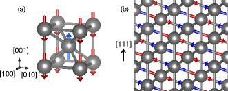
Bulk Cr follows a bcc crystal structure with lattice parameter =2.91 Å. Each atom has 8 nearest neighbors (n.n.s). Surfaces perpendicular to the [111] direction exhibit three-fold C3 symmetry and an open structure, since only 6 out of the 8 n.n.s lie in the adjacent atomic layers, while the remaining 2 n.n.s are located three atomic layers above and below. Along this direction the stacking sequence follows an …ABCABC… pattern, analogous to that of the Bi2Se3 crystal in the [0001] direction (see Figure 1). Cr is unique among the 3 transition metals, showing an itinerant antiferromagnetic ground state. It exhibits a spin density (SDW) wave along the [100] direction –or, equivalently, along the [111] direction–, with a wave vector almost commensurate with the lattice, being its Néel temperature TN =311 K. Contrary to what happens in bulk crystals, in which all three crystallographic directions are equivalent, in thin Cr films the SDW wave vector is perpendicular to the film surface and the SDW is commensurate with the lattice. Since the Cr–Bi2Se3 systems studied are formed of a maximum of 3 Cr layers, we can consider Cr as a pure antiferromagnet in the ultrathin film regime. Thus, the Cr slabs are expected to show atoms in the same atomic layer coupled ferromagnetically, being the interlayer coupling antiferromagnetic.
We model the Cr–Bi2Se3 interfaces by 111 and 211 supercells with the equilibrium in–plane lattice constant of bulk Bi2Se3. We take the [0001] Bi2Se3 direction as and the (111) plane as the plane. Along the direction the supercells contain the Cr film on top of either 4 or 6 QLs (20 or 30 atomic planes) of Bi2Se3 and a vacuum layer larger than 20 Å to avoid interaction between opposite surfaces. During the structure optimization, the Cr overlayers and the interfacemost QL of Bi2Se3 were fully relaxed until the residual forces were smaller than 0.02 eV/Å, while the remaining atoms were fixed to the relaxed geometry of the corresponding Bi2Se3 thin film.
III Atomic Structure and interface charge transfer
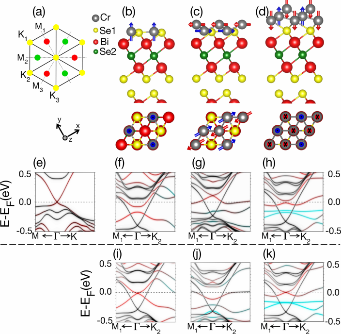
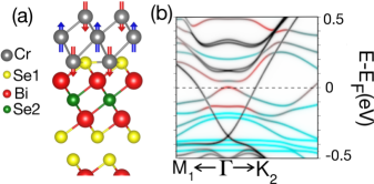
We consider commensurate Cr films with 1, 2 and 3 ML thicknesses on top of (111) Bi2Se3 surfaces. The atomic structure of the (111) composed slab exhibits three-fold C3 symmetry and three reflection planes perpendicular to the surface –see Fig. 2 (a)–. The in–plane lattice parameters of Bi2Se3 (4.14 Å) and Cr (4.12 Å) show a small lattice mismatch of 0.5%. First, we examine different positions for the Cr overlayers, including fcc and hcp hollow sites, bridge and Se-top sites. As expected, the high symmetry hollow sites are the energetically most favorable. Figures 2 (a) to (d) show the calculated equilibrium structures. For 1 and 2 ML films the interfacial Cr atoms occupy the fcc hollow sites following the Bi2Se3 stacking, …-BcAbC-A and …-BcAbC-AB respectively, where bold letters correspond to Cr atoms. However, for the 3 ML film the interface Cr moves into the hcp hollow site on top of the Bi subsurface layer and there is a reversal of the stacking sequence Aramberri et al. (2015), …-BcAbC-BAC. This spatial self–organization of the Cr film has to be due to the peculiar open structure of the (111) bcc surface in which first n.n.s are in the adjacent layers and in the third layers above and below. In this way, while for the 1 and 2 ML Cr films the interface Cr atoms are almost coplanar to the surface Se and lie on top of the Se in the center of the first QL, for the 3 ML film the Cr-Se interface bond distance increases notably and the Cr at the interface lies on top of the outermost Bi. The relaxed bond lengths are given in Table 1. The Cr-Cr distances are close to the bond lengths in bulk Cr, 2.49 Å. Note the increase in the Cr1-Se1 bond length for the 3 ML film. Additionally, the bond distances for the non-equilibrium Cr trilayer in the fcc configuration –see Fig. 3 (a)– are presented at the bottom of the Table. In this configuration, similar to the 1 and 2 ML cases, the interface Cr atoms remain almost coplanar to the Se surface at the expense of very large n.n.s Cr-Cr bond distances. The fcc configuration is about 80 meV more energetic than the equilibrium 3 ML Cr-Bi2Se3 structure, well above the energy involved in room temperature fluctuations.
The calculated binding energies are also given in the Table. The binding energy is obtained as
| (1) |
where is the total energy for the composed Cr–Bi2Se3 system, is the total energy of the isolated 4 QL Bi2Se3 system and is the total energy of the isolated Cr subsystem in the same ionic and magnetic configuration as it acquires in the composed Cr-Bi2Se3 system. We found a negative value for the adhesion energy for all the Cr films in correspondence with the exothermic character of dilute Cr adsorbed on Bi2Se3 surfaces for submonolayer coverages Abdalla et al. (2013); Wang et al. (2015).
| Cr3-Cr2 | Cr2-Cr1 | Cr1-Se1 | ||
|---|---|---|---|---|
| 1 ML | - | - | 2.39 | -2.00 |
| 2 ML | - | 2.59 | 2.40 | -1.98 |
| 3 ML | 2.64 | 2.48 | 2.84 | -1.77 |
| 3 ML-fcc* | 3.11 | 3.42 | 2.39 | -1.69 |
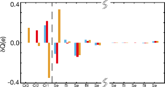
The different atomic configuration of the equilibrium structures is clearly reflected in the interface charge redistribution. We have calculated the Mulliken charges for the Cr–Bi2Se3 systems and for the corresponding isolated slabs, a pristine 4 QL Bi2Se3 slab, and the isolated Cr films of 1, 2 and 3 Cr MLs with the same atomic and magnetic configuration as they present when adhered to Bi2Se3 . The differences between the Mulliken charges of the entire Cr–Bi2Se3 systems and those corresponding to the isolated subsystems are displayed in Figure 4. In all the cases the charge transfer is small and mostly confined to the Cr film and the first Bi2Se3 QL. For 1 and 2 Cr ML coverages, the Cr layers acquire charge at the expense of the Se atoms, both at the interface and in the middle of the first QL. In the 3 Cr ML system, on the contrary, the charge transfer is towards the Bi2Se3 . The interfacial Cr donates charge, mainly to the n.n.s. Se, which gains electron charge, increasing its ionic radius and consequently increasing the interface bond length. This different behavior can be attributed to the different adsorption site of the first Cr layer (hcp hollow versus fcc hollow for 1 and 2 Cr MLs). Nevertheless, there is always a chemical interaction at the interface. In addition, the Bi2Se3 free surface presents a small charge gain in all the calculated structures.
IV Magnetic ground state
To model the magnetic ground state of Cr layers we consider different configurations having parallel and antiparallel collinear Cr magnetizations both between planes and within a plane. We employed an in–plane unit cell with 2 atoms per plane. We find a ferrimagnetic ground state with ferromagnetic Cr planes coupled antiferromagnetically for all the studied Cr film thicknesses.
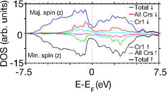
Due to the C3 symmetry of both Cr and Bi2Se3 layers, the 3 Cr and 4 Se orbitals hybridize, as can be clearly appreciated in the spin–resolved total DOS for three Cr layers adhered to Bi2Se3 shown in Fig. 5. The hybridization drives the Cr states close to the Fermi level, confined in an energy region 1.5 eV below EF. In addition, a large energy splitting of about 4 eV between the spin–majority and the spin–minority states is obtained, and the majority Cr states are fully occupied while the minority–spin channel is almost unoccupied. Therefore, the magnetic moments (MMs) of the Cr layers are close to the Hund rule value for isolated Cr atoms. The calculated MMs, shown in Table 2, are remarkably large at the surface plane ( 4 /atom) for all the systems, while they decrease for the subsurface Cr layers. For 1 and 2 ML Cr films there is an appreciable induced MM on the Se and Bi topmost planes of 0.2 , aligned opposite to the Cr MM at the interface, while the induced MMs in the Bi2Se3 for the 3 ML Cr film is almost negligible in correspondence with the different chemical interaction at the interface. Note the larger MMs of the 3 ML Cr fcc structure due to larger interlayer distances.
| 1 ML | - | - | 4.3 | 4.0 |
| 2 ML | - | 4.2 | -3.1 | 1.4 |
| 3 ML | -4.2 | 3.6 | -3.7 | -4.3 |
| 3 ML-fcc* | -4.9 | 4.7 | -4.0 | -3.8 |
Since the spin–orbit coupling is included in the calculations we can determine the direction of the Cr MM relative to the crystal lattice. The preferential orientation of the Cr magnetization vector was obtained by comparing the total energies of in–plane (, ) and out–of–plane () orientations of the total magnetization (the axis is defined normal to the surface). It is noteworthy to point out that in the ground state within the planes the Cr atoms are always coupled ferromagnetically, thus the Cr MMs are aligned within each layer–see Fig. 2 (a)–.
The easy magnetization axis for the 1 ML Cr–Bi2Se3 system lies perpendicular to the surface (out–of–plane), while as the thickness of the Cr film increases a double spin reorientation transition takes place and the magnetization direction changes to in–plane for 2 ML and again to out–of–plane for the 3 ML Cr film. A similar spin reorientation transition has been reported in ultrathin Co films grown on hexagonal Ru (0001) El Gabaly et al. (2006). The magnetic anisotropy for the 1 and 2 ML Cr–Bi2Se3 systems is unusually large, of 25 meV and 35 meV respectively, while for the 3 ML Cr–Bi2Se3 system we obtain a smaller value of 5 meV.
V Topological surface states
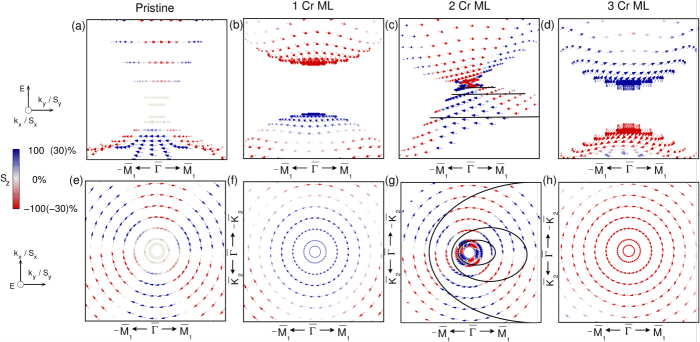
We additionally analyze the electronic structure of the Cr–Bi2Se3 slabs. Figures 2 (e) to (h) show the corresponding band dispersions around the point and that of the pristine Bi2Se3 4 QL film. The band dispersion of the pristine film shows the topologically protected metallic surface states with the Fermi level located at the Dirac point. However, for all the Cr–Bi2Se3 slabs the position of the Fermi level is shifted up between 0.2 and 0.4 eV with respect to the Dirac cone of the free Bi2Se3 surface, which persists in the three cases. As a result the free surface topological SSs are always electron doped.
Next, we focus on the SS when a single Cr overlayer is adhered to the Bi2Se3 surface. A large Dirac gap opens up, and the gap opening only occurs at the interface with the magnetic film while the Dirac cone at the free Bi2Se3 surface remains, evidencing the spatially localized character of the effect. Furthermore, our calculations reveal that the magnetic easy axis is along the out–of–plane direction as shown in Fig. 2 (b). Therefore, the origin of the gapped Dirac point is the exchange coupling between the TI SS and the out–of–plane magnetization of the Cr film, which breaks TRS.
As explained above, in the 2 ML system the Cr layers present an in–plane magnetization, and we do not find any appreciable energy difference when the in–plane magnetization is along or normal to the vertical reflection planes of the Bi2Se3 thin films –see Figure 2 (a)–. Thus, we discuss the results for the in–plane magnetization normal to the reflection plane M1. The corresponding band dispersion around the point is represented in Figure 2 (g). The topological surface state survives and there is no shift in momentum space of the Dirac point, which remains at . However, the dispersion is no longer linear and the SS presents a large anisotropic mass. Only along the -K2––K2 line, perpendicular to the mirror plane, electrons at and have the same energy. The preservation of the Dirac point can be easily understood considering that although the breaking of TRS occurs for any non–zero magnetization, the slab is invariant under a reflection normal to the in–plane magnetization direction, thus the reflection symmetry M1 survives. This result is a clear demonstration that in order to open a gap at the Dirac cone, breaking the TRS and the three reflection symmetries M1,2,3 of the Bi2Se3 lattice is required Liu et al. (2013). As in the 1 ML system, the Dirac cone at the free surface of Bi2Se3 remains unmodified but for an energy shift.
For the system consisting of 3 MLs of Cr on top of the Bi2Se3 thin film, the magnetization points again along the out–of–plane direction. Therefore, its behavior is analogous to that of the 1 Cr ML slab: a gap opens at the original Dirac point, although the gap is smaller. Moreover, it is worth to note that for 3 Cr MLs, the Fermi level lies exactly within the gap of the surface Dirac fermions gapped by the exchange interaction.
For comparison, we have additionally included the dispersion relations of the 1, 2 and 3 Cr-Bi2Se3 systems with the magnetization of the Cr layers aligned perpendicular to that of the corresponding magnetic ground states, i.e. in–plane along for the 1 and 3 ML Cr and out–of–plane along for the 2 ML Cr case –Fig. 2 (i) to (k)–. Now, the behavior of the topological SS is just the opposite, which confirms the correlation between the opening of the gap at the Dirac point and the presence of a perturbation that breaks both TRS and the invariance of the system under the three reflection symmetries of the Bi2Se3 lattice. The crossing of the topological SS persists whenever the magnetization is aligned in–plane and perpendicular to a reflection plane, as in the 1 and 3 Cr ML systems –Fig. 2 (i) and (k)–. In both cases the reflection symmetry M1 is preserved. On the contrary, a gap opens for the out–of–plane 2 ML Cr film, where TRS and the three reflection symmetries M1,2,3 are broken. The mass enhancement and the induced anisotropy in the topological SS for the 1 and 3 Cr MLs are also clearly appreciable. Moreover, the origin of the large calculated MAE is evident from the sharp contrast between the band structures of these excited states – Fig. 2 (i) to (k)– and their corresponding magnetic ground states – Fig. 2 (f) to (h)–. Finally, the band structure of the non-equilibrium 3 ML Cr film with the fcc stacking is shown in Fig. 3 (b). As expected, there is a gap opening due to the out–of–plane magnetization, analogous to that developed in the equilibrium 3 ML Cr-Bi2Se3 structure –see Fig. 2 (h)–.
These results prove that the gap opening of the topological surface states is exclusively due to the interplay of the topology and the induced magnetization, and independent of the chemical behavior. As remarked above the 1 and 2 ML Cr-Bi2Se3 systems show similar interface chemical interactions –the charge transfer has the same sign and similar value– and opposite to the interface interaction in the 3 ML slab (see Figure 4). Nevertheless, there is a gap in the 1 and 3 ML Cr-Bi2Se3 systems, while in the 2 ML Cr-Bi2Se3 structure the degeneracy of the topological SS at the point remains.
VI Spin Texture of the Surface States
As shown above, the magnetization of the Cr layers attached to the surface of the Bi2Se3 film provides a local magnetic field, which modifies the degeneracy and topology of the SS. Additionally, it induces a spin component along the magnetization direction and alters the spin texture of the topological SS. We examine the spin texture of the SSs in the equilibrium Cr–Bi2Se3 systems close to by calculating the expected value of the spin operator. The results are displayed in Figure 6, which also includes the spin distribution of the Dirac cone states of the pristine Bi2Se3 surface. For the latter the spin is locked perpendicular to crystal momentum, showing the distinct helical spin texture protected by TRS, and Sz vanishes close to the Dirac point. At large there is, however, a finite small Sz component due to the trigonal warping. Sz remains null along the mirror lines -M and reverses its sign traversing from K to -K, in correspondence with the trigonal symmetry of the system.
The spin texture of the gapped topological SSs (1 and 3 ML Cr systems) is in sharp contrast to that of the free surface. In the vicinity of the gapped Dirac point, the states show an imbalance between Sz and -Sz at a given energy, and they present a significant net out–of–plane spin polarization. Only the in–plane components reverse sign changing from to -. Furthermore, the upper and lower Dirac bands have opposite Sz, evidencing that the spin degeneracy is indeed lifted at the point. For larger , away from , the induced Sz component gradually decreases, and the out–of–plane spin distribution results from the competition between the magnetic order that aligns the spin along the out–of–plane direction and the spin texture imposed by the warping term which forces adjacent K points to have opposite Sz. In the 2 ML Cr slab, the in–plane magnetization exhibited by the Cr layers in the interfacial plane does not induce observable spin reorientations of the Dirac state, and its spin texture is analogous to that of the free surface Dirac cone. However, due to the large anisotropy of the effective mass, the constant energy lines are no longer circular, but present an elliptical shape. Nevertheless, the SSs exhibit a well defined spin helicity and the total spin cancels in every constant energy contour. TRS breaking is evident from the spin texture of the three Cr–Bi2Se3 systems analyzed.
VII Conclusions
In summary, we have found that the structural configuration of ultrathin Cr films attached to the (111) surface of Bi2Se3 is determinant to establish the topological behavior of Bi2Se3 SSs. Due to the coupling between Cr 3 orbitals and the Bi2Se3 electrons, the Cr interface induces simultaneous charge and magnetic doping. However, the properties of the topological SS critically depend on the Cr film thickness and are independent of the specific chemical interaction at the Cr-Bi2Se3 interface. As the thickness of the Cr film increases stepwise from one to three MLs, the magnetization of the Cr layers undergoes two reorientation transitions, and changes from out–of–plane (1 ML) to in–plane (2 ML) and to out–of–plane (3 ML) once again. For the 1 ML and 3 ML Cr–Bi2Se3 interfaces the magnetic overlayer induces a gap at the Dirac point, producing massive fermions at the interface. Moreover, the gap already opens for a single Cr ML, and the value of the gap depends on the absolute value of the exchange interaction. In contrast, for the 2 ML Cr system the gapless Dirac cone is preserved. The complexity of the spin texture of gapped Dirac states signifies a competition between the in–plane helical component of the spin dictated by the spin–orbit coupling and the out–of–plane TRS breaking component induced by the proximity to the magnetic Cr. Our results evidence the importance of the actual structural configuration of the magnetic films and show that the thickness of the Cr film can be used to modify in a controlled way the metallic or gapped nature of topological Dirac states and their associated spin texture.
Acknowledgments
This work has been supported by the Spanish Ministry of Economy and Competitiveness through Grants MAT2012-38045-C04-04 and MAT2015-66888-C3-1-R. We acknowledge the use of computational resources of CESGA, Red Española de Supercomputación (RES) and the i2BASQUE academic network. We also acknowledge J.I. Cerdá for fruitful discussions.
References
- Yu et al. (2010) R. Yu, W. Zhang, H.-J. Zhang, S.-C. Zhang, X. Dai, and Z. Fang, Science 329, 61 (2010).
- Qi et al. (2008) X.-L. Qi, T. L. Hughes, and S.-C. Zhang, Phys. Rev. B 78, 195424 (2008).
- Zhang et al. (2009) H. Zhang, C.-X. Liu, X.-L. Qi, X. Dai, Z. Fang, and S.-C. Zhang, Nature Physics 5, 438 (2009).
- Zhang et al. (2010) W. Zhang, R. Yu, H.-J. Zhang, X. Dai, and Z. Fang, New Journal of Physics 12, 065013 (2010).
- Chang et al. (2013) C.-Z. Chang, J. Zhang, X. Feng, J. Shen, Z. Zhang, M. Guo, K. Li, Y. Ou, P. Wei, L.-L. Wang, et al., Science 340, 167 (2013).
- Essin et al. (2009) A. M. Essin, J. E. Moore, and D. Vanderbilt, Phys. Rev. Lett. 102, 146805 (2009).
- Choi et al. (2011) Y. H. Choi, N. H. Jo, K. J. Lee, J. B. Yoon, C. Y. You, and M. H. Jung, Journal of Applied Physics 109, 07E312 (2011).
- Hor et al. (2010) Y. S. Hor, P. Roushan, H. Beidenkopf, J. Seo, D. Qu, J. G. Checkelsky, L. A. Wray, D. Hsieh, Y. Xia, S.-Y. Xu, D. Qian, M. Z. Hasan, N. P. Ong, A. Yazdani, and R. J. Cava, Phys. Rev. B 81, 195203 (2010).
- Cha et al. (2010) J. J. Cha, J. R. Williams, D. Kong, S. Meister, H. Peng, A. J. Bestwick, P. Gallagher, D. Goldhaber-Gordon, and Y. Cui, Nano Letters 10, 1076 (2010).
- Qin and Zhang (2014) W. Qin and Z. Zhang, Phys. Rev. Lett. 113, 266806 (2014).
- Liu et al. (2015a) W. Liu, L. He, Y. Xu, K. Murata, M. C. Onbasli, M. Lang, N. J. Maltby, S. Li, X. Wang, C. A. Ross, P. Bencok, G. van der Laan, R. Zhang, and K. L. Wang, Nano Letters 15, 764 (2015a).
- Sitte et al. (2012) M. Sitte, A. Rosch, E. Altman, and L. Fritz, Phys. Rev. Lett. 108, 126807 (2012).
- Chen et al. (2010) Y. L. Chen, J.-H. Chu, J. G. Analytis, Z. K. Liu, K. Igarashi, H.-H. Kuo, X. L. Qi, S. K. Mo, R. G. Moore, D. H. Lu, M. Hashimoto, T. Sasagawa, S. C. Zhang, I. R. Fisher, Z. Hussain, and Z. X. Shen, Science 329, 659 (2010).
- Haazen et al. (2012) P. P. J. Haazen, J.-B. Laloë, T. J. Nummy, H. J. M. Swagten, P. Jarillo-Herrero, D. Heiman, and J. S. Moodera, Applied Physics Letters 100, 082404 (2012).
- Chang et al. (2014) C.-Z. Chang, P. Tang, Y.-L. Wang, X. Feng, K. Li, Z. Zhang, Y. Wang, L.-L. Wang, X. Chen, C. Liu, W. Duan, K. He, X.-C. Ma, and Q.-K. Xue, Phys. Rev. Lett. 112, 056801 (2014).
- Cha et al. (2012) J. J. Cha, M. Claassen, D. Kong, S. S. Hong, K. J. Koski, X.-L. Qi, and Y. Cui, Nano Letters 12, 4355 (2012).
- Figueroa et al. (2014) A. I. Figueroa, G. van der Laan, L. J. Collins-McIntyre, S.-L. Zhang, A. A. Baker, S. E. Harrison, P. Schönherr, G. Cibin, and T. Hesjedal, Phys. Rev. B 90, 134402 (2014).
- Kou et al. (2012) X. F. Kou, W. J. Jiang, M. R. Lang, F. X. Xiu, L. He, Y. Wang, Y. Wang, X. X. Yu, A. V. Fedorov, P. Zhang, and K. L. Wang, Journal of Applied Physics 112, 063912 (2012).
- Kou et al. (2013) X. Kou, L. He, M. Lang, Y. Fan, K. Wong, Y. Jiang, T. Nie, W. Jiang, P. Upadhyaya, Z. Xing, Y. Wang, F. Xiu, R. N. Schwartz, and K. L. Wang, Nano Letters 13, 4587 (2013).
- Zhang et al. (2012) J.-M. Zhang, W. Zhu, Y. Zhang, D. Xiao, and Y. Yao, Phys. Rev. Lett. 109, 266405 (2012).
- Zhang et al. (2013) J.-M. Zhang, W. Ming, Z. Huang, G.-B. Liu, X. Kou, Y. Fan, K. L. Wang, and Y. Yao, Phys. Rev. B 88, 235131 (2013).
- Liu et al. (2015b) W. Liu, D. West, L. He, Y. Xu, J. Liu, K. Wang, Y. Wang, G. van der Laan, R. Zhang, S. Zhang, and K. L. Wang, ACS Nano 9, 10237 (2015b).
- Wang et al. (2015) E. Wang, P. Tang, G. Wan, A. V. Fedorov, I. Miotkowski, Y. P. Chen, W. Duan, and S. Zhou, Nano Letters 15, 2031 (2015).
- Soler et al. (2002) J. M. Soler, E. Artacho, J. D. Gale, A. García, J. Junquera, P. Ordejón, and D. Sánchez-Portal, Journal of Physics: Condensed Matter 14, 2745 (2002).
- Cerdá et al. (1997) J. I. Cerdá, M. A. Van Hove, P. Sautet, and M. Salmeron, Phys. Rev. B 56, 15885 (1997).
- Cuadrado and Cerdá (2012) R. Cuadrado and J. I. Cerdá, Journal of Physics: Condensed Matter 24, 086005 (2012).
- Kresse and Hafner (1993) G. Kresse and J. Hafner, Phys. Rev. B 48, 13115 (1993).
- Perdew et al. (1996) J. P. Perdew, K. Burke, and M. Ernzerhof, Phys. Rev. Lett. 77, 3865 (1996).
- Ortmann et al. (2006) F. Ortmann, F. Bechstedt, and W. G. Schmidt, Phys. Rev. B 73, 205101 (2006).
- Aramberri et al. (2015) H. Aramberri, J. I. Cerdá, and M. C. Muñoz, Nano Letters 15, 3840 (2015).
- Abdalla et al. (2013) L. B. Abdalla, L. Seixas, T. M. Schmidt, R. H. Miwa, and A. Fazzio, Phys. Rev. B 88, 045312 (2013).
- El Gabaly et al. (2006) F. El Gabaly, S. Gallego, C. Muñoz, L. Szunyogh, P. Weinberger, C. Klein, A. K. Schmid, K. F. McCarty, and J. de la Figuera, Phys. Rev. Lett. 96, 147202 (2006).
- Liu et al. (2013) X. Liu, H.-C. Hsu, and C.-X. Liu, Phys. Rev. Lett. 111, 086802 (2013).