Two-dimensional plasmons
in lateral carbon nanotube network structures
and
their effect on the terahertz radiation detection
Abstract
Keywords: carbon nanotube network, Schottky contact, two-dimensional carrier system, terahertz radiation, plasmonic resonance
We consider the carrier transport and plasmonic phenomena in the lateral carbon nanotube (CNT) networks forming the device channel with asymmetric electrodes. One electrode is the Ohmic contact to the CNT network and the another contact is the Schottky contact. These structures can serve as detectors of the terahertz (THz) radiation. We develop the device model for response of the lateral CNT networks which comprise a mixture of randomly oriented semiconductor CNTs (s-CNTs) and quasi-metal CNTs ( m-CNTs). The proposed model includes the concept of the two-dimensional plasmons in relatively dense networks of randomly oriented CNTs (CNT ”felt”) and predicts the detector responsivity spectral characteristics. The detection mechanism is the rectification of the ac current due the nonlinearity of the Schottky contact current-voltage characteristics under the conditions of a strong enhancement of the potential drop at this contact associated with the plasmon excitation. We demonstrate that the excitation of the two-dimensional plasmons by incoming THz radiation the detector responsivity can induce sharp resonant peaks of the detector responsivity at the signal frequencies corresponding to the plasmonic resonances. The detector responsivity depends on the fractions of the s- and m-CNTs. The burning of the near-contact regions of the m-CNTs or destruction of these CNTs leads to a marked increase in the responsivity in agreement with our experimental data. The resonant THz detectors with sufficiently dense lateral CNT networks can compete and surpass other THz detectors using plasmonic effects at room temperatures.
I Introduction
Plasmonic electron phenomena in semiconductors could enable advanced terahertz (THz) devices 1 ; 2 . In particular, the THz detectors using the non-linear plasmonic properties of two-dimensional electron gas (2DEGs) 2 have proved to be very effective devices operating at room temperature 3 ; 4 ; 5 ; 6 ; 7 ; 8 ; 9 ; 10 ; 11 ; 12 ; 13 ; 14 ; 15 ; 16 ; 17 ; 18 ; 19 ; 20 ; 21 . The resonant excitation of the plasma oscillations in the gated and ungated 2DEGs by incoming THz radiation could support relatively large electric-field oscillations and, hence, rather large rectified current components. Using the nonlinearity of the current-voltage characteristics (such as the nonlinearity of the thermionic or tunneling channel-gate leakage or injection currents) to enhance the hydrodynamic nonlinearity of plasma oscillations 2 ; 22 ; 23 ; 24 ; 25 ; 26 ; 27 ; 28 ; 29 , the pertinent detectors can exhibit marked advantages. In particular, the combination of the plasmonic properties of the 2DEG channel with the contact nonlinearity can be realized in lateral Schottky diodes 24 ; 25 .
The detection of THz radiation in lateral device structures based on carbon nanotubes (CNTs) was demonstrated in Refs. 30 ; 31 ; 32 ; 33 ; 34 . The detection mechanisms in the devices with nonuniform CNT networks 32 ; 33 ; 34 are associated with nonuniform heating of the electron or hole system by the absorbed THz radiation or with the structure asymmetry due to metal contacts with different nonlinear properties leading to the rectification of the ac current induced by this radiation. Different CNT-base photodetectors and mechanisms of their operation were reviewed in Ref. 35 The incident THz radiation can excite the plasma oscillations in lateral CNT networks (with the wavelength larger that the average distance between the CNTs) in a similar way as in the 2DEG channels in the standard heterostructures or in the graphene-based heterostructures. The plasmonic nature of the THz response in CNT systems was discussed in a number of publications (see, for example, Refs. 36 ; 37 ; 38 ; 39 ; 40 ). The role of the plasmonic effects in the aligned CNTs and disordered CNT networks was experimentally confirmed in Refs. 41 ; 42 ; 43 ; 44 . The interpretation of the experimental findings, relied on the concept of 1D plasmons propagating along the CNT and having cylindrical symmetry of the potential distribution (see, for example, Ref. 37 ). However, in sufficiently dense lateral CNT, different CNTs interact with each other and, as a result, the plasma oscillations excited by the THz radiation can be associated with the collective coherent motion of the carriers belonging to many CNT responding to the ac self-consistent electric fields. This collective motion reveals the 2D-nature of the response, especially pronounced when the plasma wavelength markedly exceeds the average distance between the CNTs.
In this paper, in contrast to the previous works focused on the dilute CNT systems (including the composite materials with randomly dispersed, randomly oriented CNTs), we study the 2D plasma oscillations excited by the THz radiation in lateral dense CNT disordered networks consisting of a mixture of the single-wall semiconducting CNTs (s-CNTs) and quasi-metallic CNTs (m-CNTs) of the p-type.Also, we consider the networks of relatively long CNTs connecting two highly conducting contacts with distinct properties and focus on the role of the hole collective motion, i.e., on the plasmonic effects on the THz radiation detection and the characteristics of THz detectors based on such CNT networks.
The CNT device structure with relatively dense CNT network under consideration is similar to that fabricated and studied experimentally recently (type B devices for sub-THz and THz detection 34 and for transistor applications 45 ). We demonstrate that the hole system in the lateral CNT network can be treated as a 2D hole gas (2DHG), exhibiting pronounced plasmonic properties, and that the excitation of the plasma oscillations can result in a resonant enhancement rectified current component. Such CNT-based structures can be used in uncooled CNT-detectors with elevated responsivity exploiting the rectification mechanism.
II Device model
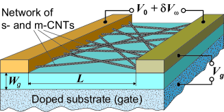
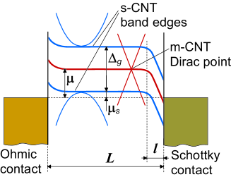
The device structure under consideration is shown in Fig. 1. We assume that the right-hand side metal (say, palladium) electrode to the lateral CNT network forms the Schottky contact (for the s-CNTs), whereas the left contact (vanadium) is virtually Ohmic. The structure is doped with acceptors. The highly conducting substrate (doped Si), separated from the CNT network by a barrier layer (SiO2), plays the role of the gate. The variation of the gate voltage provides a variation of the population of both s- and m-CNTs with carriers (holes) and a change in the average sheet charge density in the CNT network. Figure 2 shows the band diagram of the CNT structure under consideration at a negative gate voltage. The CNT array is attracted to the SiO2 layer by the Van-der-Waals forces. The CNT network (CNT ”felt”) consists of randomly oriented sufficiently long CNTs (, where and are the characteristic length of the CNTs and the spacing between the contacts, respectively), so that even those CNTs directed at rather large angles (close to ) to the direction of the source-drain current are contacted both the electrodes. The device is coupled to the THz radiation with an antenna which also serves to provide the dc and ac (induced by the incoming THz radiation) voltages between the contacts.
The ratio of the densities (per unit length in the in-plain direction parallel to the contacts)of the CNTs and m-CNTs, and , can vary in a wide range starting from to zero. The latter case corresponds to the situation when the m-CNTs are selectively destructed by applying large enough source-drain voltage at positive gate voltage with s-CNTs in non-conducting state.
For simplicity, the carrier (hole) dispersion in the s-CNTs is assumed to have a one-dimensional parabolic energy dependence on the momentum with the effective mass : The dispersion of m-CNTs can be described by the quasi-relativistic dispersion relation which in the case of small energy gap can be presented as . Here is the energy gap in the s-CNTs and cm/s is the characteristic velocity of the gapless spectrum 46 . We restrict our consideration to sufficiently dense CNT networks with a large number, , of the holes in the area with the radius equal to the Debye screening length . In this situation, the lateral carrier movement is associated with the effect of the self-consistent electric field. However, the average distance between the CNTs is assumed to be much larger than the size of the localization region around individual CNTs, so that the wave function overlap is insignificant. This allows us to consider the carrier system in each CNT as one-dimensional. The pertinent estimates will be provided in the following.
The net voltage between the source and drain contacts is equal to , i.e., it comprises the dc bias voltage and the ac THz signal voltage with the amplitude and frequency
In the presence of the ac electric field , where is the ac component of the electric potential at the CNT network plane, the ac component of hole distribution function , where is the hole momentum along the CNT and is the angle between the source-drain current direction and the CNT axis, can be found from the kinetic (Boltzmann) equation:
| (1) |
Here is the phenomenological electron scattering frequency due to the electron scattering with disorder ( and in the semiconducting and quasi-metal CNTs, respectively, is the equilibrium Fermi distribution function, and is the electron charge. In sufficiently dense CNT networks, the intersections of the CNTs can occur. In the model under consideration, these intersections are accounted for as additional scattering points for the holes propagating along the CNTs leading to an increase of the frequencies and .
II.1 Semiconducting CNT network
Generally both the electron motion along CNTs and and their polarization contribute to the ac conductivity of the CNT network. The polarization component is small because of a large energy of the bound states associated with the direction perpendicular to the CNT axis except the signal frequency close to the polarization resonant frequency 38 . As shown for the quantum wires (QWRs) of different origin 38 , , where the QWR radius. In the case of CNTs with nm, the resonant frequency is markedly large, so that the pertinent resonances can play a substantial role in the range of rather high signal frequencies which is out of scope of this work.
In the framework of a simplified model , the ac in-plane conductivity of the s-CNT network averaged over the CNT angles can be presented as
| (2) |
Here is the reduced Planck constant, is the distribution function of the CNTs over their direction angle , and . The angle distribution parameter and in the cases when all the CNTs are perpendicular to the contact and when they are uniformly distributed over the angles, respectively.
Assuming that the one-dimensional hole system in each CNT is degenerate, i.e., (the electron Fermi energy in the semiconducting CNT markedly exceeds the temperature (in the energy units). The Fermi energy is counted from the middle of the the conducting CNTs energy gap, i,e,m from the Dirac point. From Eq. (2) we obtain
| (3) |
Considering that the dc surface hole density in the semiconducting CNTs is given by the following formula:
| (4) |
Eq. (3) can be presented as
| (5) |
The appearance of a factor of () in Eq. (5) is associated with the angle spreading of the CNTs and a decreased contribution of the CNTs not parallel to the current direction.
II.2 Quasi-metallic CNT network
The ac conductivity associated with the quasi-metallic CNTs of the density can be calculated using the following expression:
| (6) |
Here . Simultaneously for the relation between the hole density in the quasi-metallic CNTs and the Fermi energy and between the ac conductivity and the hole density one can obtain
| (7) |
The quantity in degenerate electron systems with a linear dispersion is usually called as the fictituous mass.
II.3 Comparison of the ac conductivities
As follows from Eq. (6), the ac conductivity does not explicitly depend on the Fermi energy
However, (as well as ) can depend on the Fermi energy and the hole density via the dependences of the collision frequencies.
Comparing Eqs. (3) and (6), we find
| (8) |
If the collision frequency is proportional to the density of states at the Fermi level, Eq. (8) in the limits and respectively yields
| (9) |
and
| (10) |
Setting , g, and meV, we obtain and .
III Forced plasma oscillations in CNT network structures
III.1 Gated structures
For the CNT structures with the the gate layer thickness , the self-consistent ac potential at the CNT network plane can be calculated from the Poisson equation in the gradual channel approximation 47 :
| (11) |
Here is the ac variation of the net hole density in the CNT network, is the dielectric constant of the gate layer material. The axis is directed in the CNT network plane from one the contact to another and the axis is perpendicular to this plane (see Fig.1).
In Eq. (11), the quantum capacitance 48 is disregarded because for the practical values of the gate layer thickness 33 the geometrical capacitance per unit area is much smaller than the quantum capacitance.
The continuity equations of the electron components in the semiconducting and quasi-metallic CNTs can be presented in the following form:
| (12) |
| (13) |
Combining Eqs. (11) - (13), we arrive at the following equation governing the ac potential in the channel
| (14) |
where , or
| (15) |
Here
Assuming for simplicity that , Eqs. (14) and (15) can be reduced to the following:
| (16) |
Here
| (17) |
where
| (18) |
and
| (19) |
are the characteristic plasma-wave velocity and frequency of plasma oscillations in the gated channel of the length (). If and , the latter equation yield the same value for as for the 2DEG with the parabolic electron spectrum and the effective mass : .
Considering Eqs. (4), (7), and (18), can be expressed either via and or via :
| (20) |
Here . This quantity does not depend on the hole density and, hence, on the absolute value of the gate voltage , and increase in the hole density leads to an increase in the fictituous mass , so that [see Eq. (7)]. At cm-1, one obtains cm-2. It is instructive that can be both smaller and larger than real hole density in the m-CNTs depending the m-CNT density. Since the net hole density (and, what is important, the hole density in the s-CNTs) in the gated structures varies with varying gate voltage , the characteristic plasma frequency is voltage controlled. However, the dependence differ from those in the gated 2D electron or hole systems in the standard heterostructures ( 2 ) and graphene ( 49 ), because according to Eq. (21)only the variations of the hole density in the s-CNTs affect the plasma frequency.
The boundary conditions can be formulated using the following reasoning. The resistance of the left-hand-side contact (at ), which can be considered as the Ohmic one, is small so that the potential drop at this contact is negligible. In contrast, the potential drop across the right-hand-site contact depletion region, which is usually modeled as a Schottky contact (see, for example, Refs. 50 ; 51 ).
In our model, we assume that the ac current density across the depletion region is associated with the Ohmic component (characterized by the m-CNT contact resistance ), hence, the pertinent current density , with the current density through the contacts of the s-CNTs and metallic electrode (which is modelled by the Schottky-contact current-voltage characteistic) , and the density of the displacement current . Here is the resistance of the Schottky contact between each s-CNT and the electrode, is the parameter of the Schottky-contact nonlinearity, is the capacitance of the depletion region (per unit length in the lateral direction perpendicular to the current flow), and is the thickness of the depletion region at the Schottky contact [see Fig. 2]. Thus, the net current density across the contact is equal to
| (21) |
where is the contact region admittance (per unit length the current flow direction) and , so that . In the case of the blade-like electrodes, the capacitance can be estimated as , where the factor describes the specifics of the geometry the Schottky contact of the s-CNTs and the metal electrodes. )n the analogy with the Schottky contacts of 2DEG or 2DHG, 52 (see also Refs. 53 ; 54 ; 55 . In the gated structures, the net ac current between the electrodes comprises also the displacement current between them through the gate . The pertinent capacitance (per unit length) can be estimated as . At small overlap, , between the electrodes and the gate is can be disregarded. Moreover, this ac current does not affect boundary conditions (22). ,
Considering this and disregarding the nonlinear term in the expression for the current density (only in the calculation of the linear response), the boundary conditions can be set as follows:
| (22) |
Similar boundary conditions were used previously in the modeling of different plasmonic devices with the Schottky contacts 24 ; 25
Equation (16) with the boundary conditions (22) yield the following formulas for the ac potential :
| (23) |
for the range , where (with ), and
| (24) |
for . Here
| (25) |
where and is the time of the Schottky contact ”capacitor” charging via the quasi-neutral region of the CNT network.
In particular, for the ac voltage drop across the contact region which determines the rectified current Eqs. (23) and (24) yield
| (26) |
Hence, the square of the absolute value of the ac potential drop across the depletion region averaged over the THz radiation period is given by
| (27) |
Assuming g, , , nm, and cm-2, a m, Eq. (21) yields THz. The above electron density is achieved at V (i.e., at V/cm). Considering these parameters, we also set s-1, , (this corresponds to the experimental data for purely s-CNT network), cm-1 (i.e., cm). As a result, we obtain the following estimates: and s. As seen from the results below, just the latter time determines the role of the Schottky contact capacitance in the high-frequency response.
III.2 Ungated structures
In the CNT structures under consideration with a relatively thick gate layer (), the self-consistent electric field is localized near the CNT network plane and sufficiently far from the gate. In these structures, the conductivity of the gate only weakly affects the plasma oscillations, in particular, their dispersion characteristics. Therefore, such structures can approximately be considered as the ungated ones, although a remote gate can be used for the voltage control of the carrier density.
In the ungated structures, the self-consistent ac electric potential in the channel (z = 0) and in the areas surrounding it ( and , can be found from the following equation 24 ; 25 ; 52 ; 56 ; 57 :
| (28) |
Here the Dirac delta function describes the hole localization at the plane of the CNT network . Considering the hole motion along the CNTs, Eq. (28) can be transformed to the following:
| (29) |
Apart from the natural boundary conditions , the same boundary conditions as above [i.e., Eq. (22)] can be used for different point in the channel. Solving Eq. (29) with the latter boundary conditions, for the ac potential distribution in the main part of the channel we obtain
| (30) |
| (31) |
Consequently,
| (32) |
One can see that Eq. (32) coincides Eqs. (27) with the replacement of the quantities and by
| (33) |
and
| (34) |
respectively.
Here the pertinent characteristic plasma frequency is given by the following equation [different from Eq.(20)]:
| (35) |
Hence, , i.e., at the same , . For the hole density used in the estimate of in the previous subsection, the plasma frequency THz can be achieved in the ungated structures with m, i.e., in the structures with markedly longer channels. For , one obtains and .
As follows from Eq. (32), the quantity in the ungated structures (similar to that in the gated structures) can be much larger than unity at the plasmonic resonances if the quality factor of the plasma oscillations (in the ungated structures) is sufficiently large.
If the channel length and the gate layer thickness are of the same order of magnitude, Eqs. (27) and (32) are sill valid but the dispersion factors and should be replaced by the more complex unified factor.
III.3 Limiting cases
At low frequencies , , , when , from Eqs. (27) and (32), we obtain
| (36) |
If the contact resistance is small in comparison with the dc resistance of the main part of the CNT network (that can be a large number of the m-CNTs with very small contact resistance) Eq.(36) yields a very small value:
| (37) |
In real CNT networks the contact resistance can be larger than as in the CNT networks experimentally studied in Ref. 34 (see, also, Ref. 51 ). Relatively large contribution to the resistance of the contacts between quasi-metallic CNTs and the contact electrode (which could form the Schottky contact with rather low energy barrier) can be attributed to quantum contact resistance and the presence of an additional insulating barrier (not shown in Fig. 2) if no special formation methods are used 58 ; 59 .
In such a case, from Eq. (36) we obtain
| (38) |
i.e., .
At relatively large contact resistance, in a wide frequency range parameter . In this frequency region for the gated structures Eq. (27) yields
| (39) |
At very high signal frequencies, the imaginary part of the contact region admittance can become large, so that the displacement current can actually shunt the depletion region. In this frequency range, (and ) can become small. In this case,
| (40) |
Equation (40) explicitly describes a decrease in with increasing product . Hence, a decrease in with increasing frequency due to the capacitance effects is characterized by relatively short charging time .
The relationships similar to Eqs. (39) and (40) can be obtained from Eq. (32) with and instead of and .
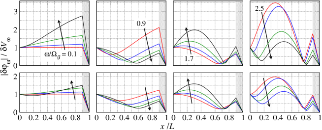
Figure 3 shows the spatial distributions of the ac potential distribution in the gated structures calculated using Eqs. (23) and (24) for different ratios at different ratios (i.e.,different values of the plasma oscillations quality factor . It is assumed that and and . If, in particular, s-,the upper and lower panels of Fig. 3 correspond to THz and THz, as well as s and s, respectively
The spatial distributions for (in two left-side upper pannels) correspond to the plasma wavelength . As seen from Fig. 3 and follows from Eqs. (23), (24), and (26), the absolute value of the ac potential can markedly exceed at the plasmonic resonances which are close to , where . In the latter cases the potential drop across the Schottky contact is large and [see Eq. (39), in which the denominator reaches a minima at the plasmonic resonances]. the distribution in two left-side panels correspond to the frequency range around the fundamental plasmonic resonance (), while two right-side panels correspond to the next resonance (). Similar situation occurs when in the ungated structures the ratio approaches to .
IV Detector responsivity
IV.1 Photocurrent
The variation of the dc current density due to the THz radiation (THz photocurrent) , which is associated with the rectified current component generated by the THz radiation, can be presented as
| (41) |
with given by Eqs. (27) or (32).
Considering that the current density across the Schottky barriers in the s-CNT-electrode junction is given by , where is the saturation current of a single-CNT junction and the height of the Schottky barrier, one can obtain . Taking this into account from Eq. (42), we obtain
| (42) |
IV.2 Current responsivity
Considering the variation of the dc current (where is the device size in the lateral direction perpendicular to the current direction) under the incoming THz radiation of intensity as the output signal, the detector current responsivity (in A/W) is defined as
| (43) |
where is the antenna aperture, is the antenna gain, and the factor ( or ) characterizes the radiation loss and reflection (effects of mismatching of the antenna and the CNT detector structure). Taking into account that , where is the speed of light and is the wavelength of the incident THz radiation, and using Eqs. (13), (16), (27), and (32), for the CNT detectors based on the gated and ungated structures we respectively obtain
| (44) |
| (45) |
Here
| (46) |
is the responsivity without the plasmonic effects. Naturally it is proportional to the density of the s-CNTs and depends on the parameters of their Schottky contact to the metal electrode ( and ). The maximum of is achieved when , i.e., when meV at room temperature.
The second terms in the right-hand sides of Eqs. (44) and (45) describe the effect of the plasma oscillations excitation by the incident THz radiation. These terms can exhibit a pronounced resonant behavior as a function of the signal frequency and the plasma frequencies (or ) provided the quality factor of the plasma oscillations is large.
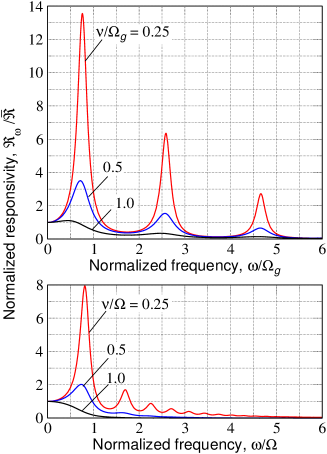
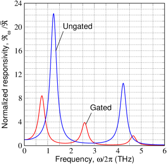
Figure 4 shows the spectral characteristics frequency dependences of the normalized current responsivity of the gated and ungated detectors calculated using Eqs. (45) and (46) respectively, with different ratios (upper panel) and (lower panel) assuming and and . As seen from Fig. 4, the responsivities of both gated and ungated detectors exhibit resonant maxima with the sharpness increasing with decreasing and (with increasing resonance quality factors). The responsivities can achieve rather high values markedly exceeding the those at low-frequencies.
As an example, Fig. 5 demonstrates the frequency dependences of the gated and ungated detector responsivity with THz and THz, respectively. These values correspond to m and m (in the gated device), m (in the ungated device), and the same hole densities ( cm-2) in both. The collision frequency is assumed to be s-1, so that s; other parameters are the same as for Fig. 4.
Both Fig. 4 and Fig. 5 show a marked shift of the resonances from their nominal values and toward smaller frequencies. Some deviation of the plasmonic resonant frequencies from and is associated with the finiteness of its depletion width () resulting in an effective shortening of the plasmonic cavity, and the plasma oscillations damping due to the hole scattering proportional to . The first reason provides some increase in the resonant frequencies [by a factor of ], while the second effect leads to a vary decrease in the resonant frequencies in the ungated devices (see Appendix A). Both mechanisms are relatively weak at the parameters used in the calculations: and . The main contribution to a substantial decrease in the resonant frequencies is associated with the effect of the Schottky contact capacitance.
The resonant peak width is determined by the plasma resonance quality factors, and [see Eqs. (A5) and (A6) in the Appendix A]. As for the height of the resonant peaks with different index , its decrease with increasing in the gated devices is solely due to the capacitance effect characterized by the quantity . Our calculations shows an equalizing of the peak heights, whose positions tend to the nominal resonant frequencies, when the charging time and the capacitance decrease. However, in the ungated devices, lowering of the peaks associated with the capacitance effect is reinforced by entirely plasmonic mechanism. This explains a more dramatic responsivity roll-off in the ungated devices compared to the gated ones seen in Figs. 4 and 5.
IV.3 Voltage responsivity
In the absence of the applied bias voltage, the quantity can be considered as the induced photovoltage. The latter is determined by the balance between the photocurrent and the dc current density caused by the induced photovoltage . As a result, using Eq. (43), assuming that (i.e., at relatively low radiation intensities), for the voltage responsivity we find
| (47) |
where
| (48) |
From Eq. (48) we obtain that in the structures with not too small fraction of the m-CNTs in which can be rather small. In contrast, in the structures with the destructed m-CNTs or disconnected from the right contact (the Schottky contact for the s-CNTs) by the scorching (burning) of the near contact portions of the m-CNTs can be rather large. Indeed, setting , from Eq. (48) we obtain . One needs also to point out that in the former case, the current responsivity can be much smaller than in the latter case. Thus, the elimination of the m-CNTs can lead to a marked increase in the low-frequency current responsivity but even stronger relative increase in the low-frequency voltage responsivity. In principle, the elimination of the m-CNTs can result in a significant change of the plasmonic properties.
V Comparison with the experimental data
We compare the above theoretical results with the recent experimental data related to the THz detectors based on asymmetric devices with one the Ohmic and the Schottky contacts and the conduction channels are formed by lateral arrays of CNTs 34 and some new our experimental results shown below. Assuming A, , and K, we obtain A/V2, that is consistent with the experimental value 34 A/V2. For (), and , Eq. (46) yields A/W. Taking into account that in the experiments 34 and setting also , we find A/W and somewhat lower values for GHz (that is markedly smaller than the plasmonic frequency). Taking into account that , for the sub-THz frequency range we obtain V/W. These values of the current and voltage responsivities are in a reasonable agreement with the data obtained experimentally 34 . To achieve higher responsivities, the devices with higher antenna efficiency should be used. Another opportunity is to realize the resonant plasmonic response predicted above using the structures with relatively high ratios or .
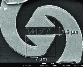
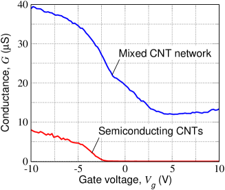
As predicted above, the elimination of the m-CNTs might also lead to a substantial increase in the responsivity. To verify this, we fabricated and measured device structures similar to those fabricated and studied as in Ref. 34 . The spacing between the contacts and the gate thickness are nm and nm, respectively. It includes eight CNTs connecting the electrodes (so that cm-1) and was supplied with a spiral antenna. The SEM image of such a CNT device is shown in Fig. 6. The structure corresponds to that schematically shown in Fig. 1. Originally the CNT network was formed with a mixture of the s- and m-CNTs. This is confirmed by the analysis of the device transfer characteristics. The response of the structure was measured at the negative gate voltage V) as a function of the radiation frequency in the sub-THz range from 140 to 220 GHz The CNT network was coupled to the radiation by a spiral antenna. Then the m-CNTs that provided a substantial current path between the electrodes were destroyed, so that the current between the electrodes was associated with the s-CNTs. The response of this structure after the destruction of of the m-CNTs was measured as a function of the radiation frequency (at the same gate voltage and in the same frequency range as in the case of original structure). The results of the transfer characteristics measurements are shown in Fig. 7. As seen from Fig. 7, the maximum device conductance (ON-conductance) at the negative gate voltage originally was about of S. After some CNTs were destroyed, the conductance droped down to S. This implies that the contribution of the destroyed m-CNTs was about of S, and that the hole density in the s-CNTs was about one fifth of the net density. The minimum conductance (OFF-conductance) of the original structure was about of S.
As seen from Fig. 8, the voltage responsivity of the device with the destructed m-CNTs in the frequency range 150 - 160 GHz is much larger (about five times) than that of the original device with a mixture of the m- and s-CNTs.
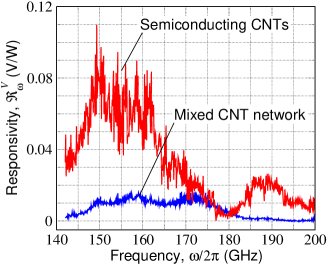
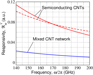
First of all, our model describes the mechanism of the THz response of the devices under consideration in terms of the rectification of the signals at the Schottky contacts of the s-CNTs and the electrode. As shown, the shunting effect caused by relatively low contact resistance of m-CNTs can substantially suppress the effect of rectification. The elimination (disconnection from the electrode or destruction) of the CNTs lead to an efficient increase in the responsivity. This is confirmed by the data shown in Fig. 8.
Second, the device model developed above predicts the resonant response of the CNT devices under consideration to the THz radiation associated with the excitation of the 2D-plasmons.
Although the experimental data shown in Figs. 7 and 8 are related to rather delute CNT networks, we apply the obtained above formulas for, at least, qualitative consideration of the experimental situation.
Since the gate layer thickness nm is close the quantity nm, , so that both Eqs. (21) and (36) can be used for rough estimates. There are two plausible scenario: (a) due to burning, the m-CNTs are disconnected from the electrode, which forms the Schottky contacts with the s-CNTs, and (b) the m- CNTs are fragmented into small fractions much shorter than the spacing between the electrodes.
In the case ”a”, the holes belonging to the both types of the CNTs contribute to the plasma frequencies and . The analysis of the measurement results provides the hole density induced by the gate voltage V about of cm-2. The acceptor-induced hole density could be roughly estimated from the threshold gate voltage (, see Fig. 6) to be about cm-2. Setting , g, , V, and cm-2, from Eqs. (20) and (35) we obtain GHz. In contrast, in the case ”b”, when only the holes in the s-CNTs determine the plasma frequencies, assuming cm-2, we arrive at GHz.
We calculated the current and voltage responsivities of the detectors with the above parameters in a wide range of hole collision frequencies . Figure 9 shows an example of the voltage responsivity as a function of the signal frequency calculated using Eqs. (44) - (48) for the CNT structures with a mixture of the m- and s-CNTs with GHz and for the CNT structure with disconnected m-CNTs with GHz) as well as fragmented m-CNTs with GHz assuming the hole collision frequency s-1 and the pertinent charging time s . In line with Fig. 7, it is also assumed that the ratio of the conductance for the structure with the CNT mixture and for the structure with destroyed m-CNTs is equal to five. According to Fig. 9 (as well as according to the calculations with other values of ), the frequency dependences of the voltage responsivity are monotonically decreasing not exhibiting any resonant peaks. This can be attributed to relatively low quality factor ( in the case of fragmented m-CNTs) and to the signal frequencies well below the plasmonic resonance frequency in the case of the mixed CNT array and the array with disconected m-CNTs). Due to this, t the responsivity maxima in Fig.8 are most probably attributed to to antenna shape -induced effects.
VI Discussion
VI.1 Self-consistent 2D model
As it was assumed in the model under consideration, each electrons interact with a large number of others. This is in line with the consideration of the collective effects in different plasmonic media with a large number of charged particles in the Debye sphere 60 .
In our case, assuming for simplicity that the Debye screening length is the same as in the standard 2DEG with effective (or fictituous) mass g, , and cm-2, for the number of the electron inside the region with the area (inside the ”Debye circle”) we find . Setting cm-2, we obtain . However, one needs to point out that the effects of the self-consistent electric field can really be important in different plasmas even if the parameter of ideality .
The value cm-2 (which is determined either by the gate voltage and doping level) can correspond to cm-1. The quantity cm-1 implies that the average distance between CNTs is about of nm, which is orders of magnitude larger that the size of the electron localization around the CNTs (slightly larger than the diameter the CNTs under consideration nm), so that the overlap of the electron wave functions of individual CNTs is negligible. As was mentioned above, the crossing of the CNTs, at which the CNTs touch each other, can play the role of the electron scattering (collision) points. Due to the deformation mechanism of such scattering the effective collision frequency is smaller than the frequency of the crossing of these points by electrons. For cm-1 and the average electron velocity along the CNTs cm/s, this yields for the pertinent collision frequency the following estimate: s-1. The interaction of the electrons belonging to different CNTs near the crossing of the latter, does not change the momentum of the pairs of colliding electrons, and, hence, does not contribute to the electron momentum relaxation and the quantity . The latter implies that the ”crossing” collision mechanisms in question should not suppress the plasmonic resonant response when THz.
VI.2 Bolometric mechanism
The absorption of the THz radiation in the CNT network and similar sistemscan lead to a heating of the hole system in the CNTs (see, for example, Refs. 61 ; 62 ; 63 ; 64 . The excitation of the plasmonic oscillation can result in the enhancement of the absorption at the plasmonic resonances. In this case, apart from the rectified current, an extra dc current associated with the difference of the electron temperature in the CNT network and the contacts can appear if the contacts have different thermal properties. The calculation of the bolometric contribution to the responsivity under the conditions of the plasmonic effects, requires a more complex model than that used above. The spatial distribution of the effective hole temperature might be essentially nonuniform due to the nonuniform spatial distribution of the ac electric field (which heats the DHG in the CNT network under consideration) and due to thermal flows from the CNT network toward the contacts. Therefore, the equations of more strict device model should be supplemented by the heat conductivity equation and related boundary conditions accounting for the contact properties. This model will be considered elsewhere. Below we estimate the bolometric contribution to the responsivity using a fairly simple model.
Assuming that (1) the variation of the current due to the hole heating is associated primarily with the variation of the Schottky contact electrical conductivity (due to higher thermal conductivity of the Ohmic contact and, hence, smaller temperature gradient near the latter), (2) the variation of the effective hole temperature near the Schottky contact is close to that averaged over the entirely CNT network and the plasmonic oscillation period , and (3) only the s-CNTs contribute to the effect in question. In such a situation, the expression for the density of the rectified current given by Eqs. (41) and (42) should be generalized as follows:
| (49) |
where characterized the variation of the current density trough the Schottky contact due to an increase of the hole effective temperature in the s-CNTs. Since is determined by the balance between the THz power absorbed by the CNT network and the power which goes to the lattice (and the contact), one can write , where is the effective energy relaxation time. Considering this, one can arrive at the the following formulas for the rectified current density and the net responsivity (associated with both the rectification and bolometric effects):
| (50) |
and
| (51) |
Here
| (52) |
is the ratio of the hole bolometric response and the effect of the rectification, where . Setting meV, g, and m, s-1 at THz, we obtain . This implies that can be comparable with unity or exceed it if the hole energy relaxation time is sufficiently long. According to these estimates, there should s for the sub-THz frequencies and s for the frequencies about 1 THz. At sufficiently low temperatures, the latter conditions can be satisfied.
If the hole heating leads to stronger hole current from the CNT network to the Ohmic contact due to, in particular, special thermal isolation of the pertinent CNT network (as in device A in Ref. 34 ), the bolometric responsivity can be relatively high and exhibit the opposite sign.
VII Conclusions
We investigated the hole transport and the plasmonic oscillations excited by incoming THz radiation in the device structures with lateral CNT networks and asymmetric contacts (one Ohmic contact and one Schottly contact) and evaluated their effect on the operation of the THz detectors using such structures. We developed the device models accounting for the 2D nature of the collective behavior of the hole system in lateral CNT networks, i.e., treating this system as a 2DHG, including both the s- and m-CNTs and the specifics of the contact phenomena. As demonstrated, the rectification of the ac current stimulated by the THz radiation at the Schottky contact of the s-CNTs (associated with the nonlinearity of the current-voltage characteristics of this contact) is an effective mechanism of the THz detection. The excitation of plasmonic oscillations of the self-consistent electric field by the THz radiation can lead to a substantial increase in the rectified current and, hence, to the elevated detector responsivity. Due to the resonant character of the plasmons excitation, the responsivity can exhibit sharp resonant peaks. The positions of these peaks can be controlled by the gate voltage. We showed that the disconnection (or fragmentation) of the m-CNTs from the contact electrode results in a marked increase in the responsivity due to the elimination of the partial shunting of the Schottky contact. This was confirmed experimentally by comparing the CNT structures with natural ratio of the s- and m-CNTs densities (usually two to one) with the structures with the destructed m-CNTs. The resonant THz CNT detectors with sufficiently high density s-CNT networks can surpass other THz detectors using plasmonic effects at room temperatures.
Acknowledgments
One of the authors (V.R.) is grateful to Dr. N. Ryabova for assistance. The work was supported by the Japan Society for Promotion of Science (Grant-in-Aid for Specially Promoted Research 23000008) and the Russian Scientific Foundation (Projects 14-29-00277 and 14-19-01308). G.F., I.G., and G.G. acknowledge support of the Russian Foundation for Basic Research (Grants 15-02-07787 and 15-02-07841). The works at RPI was supported by the US Army Research Laboratory Cooperative Research Agreement.
Appendix A. Lowering and smearing of resonant plasmonic peaks
In a wide range of frequencies the responsivities of the gated in ungated detectors are
| (A1) |
and
| (A2) |
respectively
Maxima of functions (A1) and (A2) are achieved at the resonant frequencies (if )
| (A3) |
and, neglecting the term ,
| (A4) |
For the broadening of the resonant peaks from Eqs. (A1) and (A2) we obtain: at
| (A5) |
and
| (A6) |
As follows from Eq. (A1), the resonant peaks height in the gated detectors is given by
| (A7) |
At , becomes proportional to a factor , so that drops as . This implies that the peaks roll-off in such devices is associated primarily with the capacitance effect characterized by the charging time . In the case of ungated devices, Eq. (A2) yields
| (A8) |
Hence, in the ungated devices, decreases with the index starting from its moderate values. At , , the capacitance effects lead to an additional roll-off of the responsivity peaks height with increasing .
References
- (1) M. Dyakonov and M. Shur, ”Shallow water analogy for a ballistic field effect transistor: New mechanism of plasma wave generation by dc current,” Phys. Rev. Lett. 71, 2465 (1993).
- (2) M. I. Dyakonov and M. S. Shur, ”Plasma wave electronics: novel terahertz devices using two-dimensional electron fluid,” IEEE Trans. Electron Devices, 43, 1640 (1996).
- (3) W. Knap, Y. Deng, S. Rumyantsev, J.-Q. Lu, M. S. Shur, C. A. Saylor, and L. C. Brunel, ”Resonant detection of subterahertz radiation by plasma waves in a submicron field-effect transistor,” Appl. Phys. Lett. 80, 3433 (2002).
- (4) T. Otsuji, M. Hanabe and O. Ogawara, ”Terahertz plasma wave resonance of two-dimensional electrons in InGaP/InGaAs/GaAs high-electron mobility transistors,” Appl. Phys. Lett. 85, 2119 (2004).
- (5) W. Knap, F. Teppe, Y. Meziani, N. Dyakonova, J. Lusakowski, F. Boeuf, T. Skotnicki, D. Maude, S. Rumyantsev and M. S. Shur, ”Plasma wave detection of sub-terahertz and terahertz radiation by silicon field-effect transistors,” Appl.Phys. Lett., 85, N 4, pp.675-677 (2004).
- (6) A. V. Antonov, V. I. Gavrilenko, E. V. Demidov, S. V. Morozov, A. A. Dubinov,J. Lusakowski, W. Knap, N. Dyakonova, E. Kaminska, A. Piotrowska, K. Golaszewska, and M. S. Shur, ”Electron transport and terahertz radiation detection in submicrometer-sized GaAs/AlGaAs field-effect transistors with two-dimensional electron gas,” Phys. Solid State, 46, pp.146-149, (2004).
- (7) J. Lusakowski, W. Knap, N. Dyakonova, L. Varani, J. Mateos, T. Gonzales, Y. Roelens, S. Bullaert, A. Cappy and K. Karpierz, ”Voltage tuneable terahertz emission from a ballistic nanometer InGaAs/InAlAs transistor,” J. Appl. Phys. 97, 064307 (2005).
- (8) F. Teppe, D. Veksler, V. Yu. Kachorovski, A. P. Dmitriev, X. Xie, X.-C. Zhang, S. Rumyantsev, W. Knap, and M. S. Shur, P”lasma wave resonant detection of femtosecond pulsed terahertz radiation by a nanometer field-effect transistor,” Appl. Phys. Lett. 87, 022102, (2005).
- (9) F. Teppe, W. Knap, D. Veksler, M. S. Shur, A. P. Dmitriev, V. Yu. Kacharovskii, and S. Rumyantsev, ”Room-temperature plasma waves resonant detection of sub-terahertz radiation by nanometer field-effect transistor,” Appl. Phys. Lett. 87, 052105 (2005).
- (10) F. Teppe, M. Orlov, A. El Fatimy, A. Tiberj, W. Knap, J. Torres, V. Gavrilenko, A. Shchepetov, Y. Roelens, and S. Bollaert, ”Room-temperature tunable detection of subterahertz radiation by plasma waves in nanometer InGaAs transistors,” Appl. Phys. Lett. 89,222109, (2006).
- (11) D. Veksler, F. Teppe, A. P. Dmitriev, V. Yu. Kachorovskii, W. Knap, and M. S. Shur Detection of terahertz radiation in gated two-dimensional structures governed by dc current Phys. Rev. B, 89, 125328, (2006).
- (12) A. El Fatimy, F. Teppe, N. Dyakonova, W. Knap, D. Seliuta, G. Valusis, A. Shcherepetov, Y. Roelens, S. Bollaert, A. Cappy, and S. Rumyantsev, ”Resonant and voltage-tunable terahertz detection in InGaAs/InP nanometer transistors,” Appl. Phys. Lett. 89, 131926 (2006).
- (13) V. I. Gavrilenko , E. V. Demidov, K. V. Marem’yanin, S. V. Morozov, W. Knap and J. Lusakowski ”Electron transport and detection of terahertz radiation in a GaN/AlGaN submicrometer field-effect transistor,” Semiconductors, 41, 2 , pp.232-234, (2007).
- (14) W. Knap, M. Dyakonov,D. Coquillat, F. Teppe, N. Dyakonova, J. Lusakowski, K. Karpierz, M. Sakowicz, G. Valusis, D. Seliuta, I. Kasalynas,A. El Fatimy, Y. M. Meziani, and T. Otsuji, ”Field effect transistors for terahertz detection: physics and first imaging applications,” J. Infrared Millimeter Terahertz Waves, 30, 1319–1337, (2009).
- (15) S. Nadar, H. Videlier, D. Coquillat, F. Teppe, M. Sakowicz, N. Dyakonova, W. Knap, D. Seliuta, I. Kašalynas, and G. Valušis, ”Room temperature imaging at 1.63 and 2.54 THz with field effect transistor detectors,” J. Appl. Phys. 108, 054508, (2010)
- (16) A. Satou, I. Khmyrova, V. Ryzhii, and M. S. Shur, ”Plasma and transit-time mechanisms of the terahertz radiation detection in high-electron-mobility transistors,” Semicond. Sci. Technol. 18, 460-469 (2003).
- (17) V. Ryzhii, A. Satou, T. Otsuji, and M.S. Shur, ”Plasma mechanism of resonant terahertz detection in a two-dimensional electron channel with split gates, J. Appl. Phys. 103, 014504 1-6 (2008).
- (18) V. V. Popov, D. V. Fateev, T. Otsuji, Y. M. Meziani, D. Coquillat, and W. Knap Plasmonic terahertz detection by a double-grating-gate field-effect transistor structure with an asymmetric unit cell Appl. Phys. Lett. 99, 243504, 2011
- (19) S.A. Boubanga Tombet, Y. Tanimoto , A. Satou , T. Suemitsu , Y. Wang , H. Minamide, H. Ito, D. V. Fateev, V.V. Popov , and T. Otsuji, ”Current driven detection of terahertz radiation in dual-grating-gate plasmonic detector Appl. Phys. Lett., 104, 262104 (2014).
- (20) Y. Kurita, G. Ducournau, D. Coquillat, A. Satou, K. Kobayashi, S.A. Boubanga-Tombet, Y.M. Meziani, V.V. Popov, W. Knap, T. Suemitsu, and T. Otsuji ”Ultrahigh sensitive sub-terahertz detection by InP-based asymmetric dual-grating-gate high-electron-mobility transistors and their broadband characteristics,” Appl. Phys. Lett., 104, 251114 (2014).
- (21) L. Vicarelli, M. S. , D. Coquillat, A. Lombardo, A. C. Ferrari, W. Knap, M. Polini, V. Pellegrini, and A. Tredicucci, ”Graphene field-effect transistors as room-temperature terahertz detectors,” Nature Mat. 11, 865 (2012).
- (22) V. Ryzhii, ”Resonant detection and mixing of terahertz radiation by induced base hot electron transistors,” Jpn. J. Appl. Phys. 37, 5937 (1998).
- (23) I. Khmyrova and V. Ryzhii, ”Resonant detection and frequency multiplication in barrier-injection heterostructure transistors,’ Jpn. J. Appl. Phys. 39, 4727-4732 (2000).
- (24) V. Ryzhii and M. S. Shur, ”Resonant terahertz detector utilizing plasma oscillations in two-dimensional electron system with lateral Schottky junction,” Jpn. J. Appl. Phys. 45, L1118 (2006).
- (25) A. Satou, V. Ryzhii, T. Otsuji, and M. S. Shur, Resonant terahertz detection antenna utilizing plasma oscillations in lateral Schottky diode, Int. J. High Speed Electron. Systems, 17, 539 (2007)
- (26) V. Ryzhii1, T. Otsuji, M. Ryzhii, and M. S. Shur, ”Double graphene-layer plasma resonances terahertz detector,” J. Phys. D: Appl. Phys. 45, 302001 (2012).
- (27) V. Ryzhii, A. Satou1, T. Otsuji, M. Ryzhii, V. Mitin, and M. S. Shur, ”Dynamic effects in double graphene-layer structures with inter-layer resonant-tunnelling negative conductivity”, J. Phys. D: Appl. Phys. 46, 315107 (2013).
- (28) D. Spirito, D. Coquillat, S.L. De Bonis, A. Lombardo, M. Bruna, A.C. Ferrari, V. Pellegrini, A. Tredicucci, W. Knap, M.S. Vitiello ”High performance bilayer-graphene terahertz detectors,” Applied Physics Letters, 104, 061111 (2014)
- (29) D. Coquillat, V Nodjiadjim, A Konczykowska, N Dyakonova, C Consejo, S Ruffenach, F Teppe, M Riet, A Muraviev, A. Gutin, M. Shur, J Godin, and W Knap, ”InP Double Heterojunction Bipolar Transistor for broadband terahertz detection and imaging systems,” J. Phys.: Conf. Ser. (2015).
- (30) H. M. Manohara, E. W. Wong, E. Schlecht, B. D. Hunt, and P. H. Siegel, Nano Lett. 5, 1469 (2005).
- (31) J. D. Chudov, D. F. Santavicca, C. B. McKitterick, D. E. Prober, and P. Kim, Appl. Phys. Lett. 100, 163503 (2012).
- (32) G. Fedorov, A. Kardakova, I. Gayduchenko, I. Charayev, B. M. Voronov, M. Finkel, T. M. Klapwijk, S. Morozov, M. Presniakov, I. 584 Bobrinetskiy, R. Ibragimov, and G. Goltsman, Appl. Phys. Lett. 103, 585 181121 (2013).
- (33) X. He, N. Fujimura, J. M. Lloyd, K. J. Erickson, A. A. Talin, Q. Zhang, W. Gao, Q. Jiang, Y. Kawano, R. H. Hauge, F. Leonard, and J. Kono, 588 Nano Lett. 14(7), 3953 (2014).
- (34) I. Gayduchenko, A. Kardakova, G. Fedorov, B. Voronov, M. Finkel, D. Jimenez, S. Morozov, M. Presniakov, and G. Goltzman, ”Response of asymmetric carbon nanotube network devices to sub-terahertz and terahertz radiation,” J. Appl. Phys. 118,194303 (2015).
- (35) X. He, F. Léonard , and J. Kono, ”Uncooled Carbon nanotube photodetectors,” Advanced Optical Materials, 3, 989 (2015).
- (36) H. E. Ruda and A. Shik, Phys. Rev. B 72, 115308 (2005).
- (37) G. Ya. Slepyan, M. V. Shuba, and S. A. Maksimenko, Phys. Rev. B 73, 195416 (2006).
- (38) A. P. Dmitriev and M. S. Shur, ”One dimensional plasmons… J. Appl. Phys. 103, 084511 (2008).
- (39) T. Nakanishi and T. Ando, J. Phys. Soc. Japan 78, 114708 (2009).
- (40) G. Ya. Slepyan, M. V. Shuba, and S. A. Maksimenko, C. Thomsen, and A. Lakhtakia, Phys. Rev. B 81, 205423 (2010).
- (41) Qi Zhang, E. H. Haroz, Z. Jin, L. Ren, X. Wang, R. S. Arvidson, A. Luttge, and J. Kono, ”Plasmonic nature of the terahertz conductivity peak in SW CNTs,” Nano Lett. 13, 5991 (2013).
- (42) X. He, W. Gao, Qi Zhang, L. Ren, and J. Kono, ”Carbon-based THz devices”-review - plasmonic response +aligned CNT + THz detectors,” Proc. SPIE 9476, 947612 (2015).
- (43) T. Morimoto, S.-K. Joung, T. Saito, D. N. Futaba, K. Hata, and T. Okazaki, ”Length-dependent plasmon resonance in single-walled Carbon nanotubes,” ACS Nano, 8, 9897 (2014).
- (44) Zh. Shi, X. Hong, H. A. Bechtel, Bo Zeng, M. C. Martin, K. Watanabe, T. Taniguchi, Y-R. Shen1, and F. Wang, ”Observation of a Luttinger-liquid plasmon in metallic single-walled carbon nanotubes,” Nat. Photonics (2015)
- (45) J. Zhang, H. Gui, B. Liu, J. Liu, Ch. Zhou, ”Comparative study of gel-based separated arcdischarge, HiPCO, and CoMoCAT carbon nanotubes for macroelectronic applications,” Nano Research, 6, 906 (2013).
- (46) R. Saito, G. Dresselhaus, and M. S. Dresselhaus, Physical Properties of Carbon Nanotubes (Imperial College Press, London, 1998).
- (47) M. S. Shur Physics of Semiconductor Devices, (Prentice Hall, Mew Jersey, 1990).
- (48) S. Luryi, Appl. Phys. Lett.52, 501 (1988). ”Quantum capacitance devices,”
- (49) V. Ryzhii, A. Satou, and T. Otsuji, ”Plasma waves in two-dimensional electron-hole system in gated graphene heterostructures,” J. Appl. Phys. 101, 024509 (2007).
- (50) Y. Noshom Y. Ohno, S. Kishinoto, and T. Mizutani, Nanotechnol. 17, 3412 (2006).
- (51) A. Vijayaraghavan, S. Kar, S. Rumyantsev, A. Khanna, C. Soldano, N. Pala, R. Vajtai, K. Kanzaki, Y. Kobayashi, O. Nalamasu, M. S. Shur, and P. M. Ajayan, J. Appl. Phys. 100, 024315 (2006).
- (52) V.Ryzhii A. Satou, I. Khmyrova, M. Ryzhii, T. Otsuji, V. Mitin, ans M.S.Shur, Plasma effects in lateral Schottky junction tunneling transit-time terahertz oscillator J. Phys. Conf. Ser. 38, 228 (2006).
- (53) B.L. Gelmont, M. S. Shur, and C. Moglestue, IEEE Trans. Electron Devices 39 1216 (1992).
- (54) D. B. Chklovskii, B. I. Shklovskii,and L. I. GlazmanI, Phys. Rev. B 46, 4026 (1992
- (55) F. Leonard and A. A. Talin, Nat. Nanotech. 6, 773 (2011).
- (56) V. Ryzhii, A. Satou, and M. S. Shur, Admittance of a slot diode with a two-dimensional electron channel” J. Appl. Phys. 93, 10041 (2003).
- (57) V. Ryzhii, A. Satou, I. Khmyrova, A. Chaplik, and M. S. Shur, ”Plasma oscillations in a slot diode structure with a two-dimensional electron channel,” J. Appl. Phys. 96, 7625 (2004).
- (58) W. King, A.Javey, R. Tu, J. Cao, O. Wang, and H.J.Dai, Appl. Phys. Lett. 87, 173 (2005).
- (59) Y. Chai, A. Hazeghi, K. Takei, H.-Y.Chen, P. C. H. Chan, A. Javey, and H.-S. Wong, IEEE Trans. Electron Devices 59, 12 (2012).
- (60) E.M. Lifshitz and L. P. Pitaevskii, Physical Kinetics ,(Elsevier, Amsterdam, 2008).
- (61) A. G. Petrov and S. V. Rotkin, Energy relaxation of hot carriers in single-wall carbon nanotubes by surface optical phonons of the substrate,” JETP Lett. 84, 156 (2006).
- (62) O. A. Dyatlova, C. Koehler, P. Vogel, E. Malic, R. M. Jain, K. C. Tvrdy, M. S. Strano, A. Knorr, and U. Woggon, ”Relaxation dynamics of carbon nanotubes of enriched chiralities,” Phys. Rev. B 90, 155402 (2014).
- (63) O. Postupna, R. Long, and O. V. Prezhdo, ”Time-domain ab initio simulation of energy transfer in double-walled Carbon nanotubes,”J. Phys. Chem. C, 119, 12088 (2015).
- (64) X. Cai, A. B. Sushkov, R. J. Suess, M. M. Jadidi, G. S. Jenkins, L. O. Nyakiti, R. L. Myers-Ward, S. Li, J. Yan, D. K. Gaskill, T. E. Murphy, H. D. Drew, and M. S. Fuhrer ”Sensitive room-temperature terahertz detection via the photothermoelectric effect in graphene,” Nature Nanotechnology 9, 814 (2014).