Observation of a nonradiative flat band for spoof surface plasmons in a metallic Lieb lattice
Abstract
We demonstrate a nonradiative flat band for spoof surface plasmon polaritons bounded on a structured surface with Lieb lattice symmetry in the terahertz regime. First, we theoretically derive the dispersion relation of spoof plasmons in a metallic Lieb lattice based on the electrical circuit model. We obtain three bands, one of which is independent of wave vector. To confirm the theoretical result, we numerically and experimentally observe the flat band in transmission and attenuated total reflection configurations. We reveal that the quality factor of the nonradiative flat band mode decoupled from the propagating wave is higher than that of the radiative flat band mode. This indicates that the nonradiative flat band mode is three-dimensionally confined in the lattice.
pacs:
81.05.Xj, 41.20.Jb, 42.25.BsI Introduction
In the terahertz (THz) region and lower frequency regions, surface plasmon polaritons confined at a metal-dielectric interface cannot exist because of the high conductivity of metals Maier (2007). However, if the surface of the metal is artificially structured, electromagnetic modes similar to the surface plasmons can be realized Maier et al. (2006); Williams et al. (2008); Pendry et al. (2004). These surface-plasmon-like modes are called spoof surface plasmon polaritons. The dispersion relation of spoof surface plasmon polaritons can be controlled by appropriately designing the structure of the metal surface Maier et al. (2006); Fernndez-Domínguez et al. (2008); Gan et al. (2008); Yu et al. (2010). Especially, if the group velocity of the spoof surface plasmon polaritons is slowed down, the plasmon-matter interaction is enhanced as is the case in light-matter interaction. To realize the slow group velocity of the spoof surface plasmon polaritons, we focus on the fact that the electron dispersion relation in crystals with specific lattice structures, such as Lieb-type Lieb (1989), Tasaki-type Tasaki (1992), and Mielke-type Mielke (1991) is independent of wave number and the group velocity becomes zero in any direction owing to destructive interference. The wave-number-independent band is called a flat band. Recently, flat bands for electromagnetic waves have been realized in photonic crystals Takeda et al. (2004); Vicencio et al. (2015); Mukherjee et al. (2015). They are also expected to exist in metallic waveguide networks Endo et al. (2010); Feigenbaum and Atwater (2010).
In previous work Nakata et al. (2012a), utilizing electrical circuit models, we showed that the dispersion relations of metal structures with various lattice symmetries have flat bands. We confirmed the formation of the electromagnetic flat bands for a metallic kagom lattice by illumination of propagating waves theoretically and experimentally Nakata et al. (2012b). In this case, however, the flat-band mode is only two-dimensionally localized in the in-plane directions and the energy escapes into free space. This is because the flat band is located inside the light cone or in a radiative region. Thus the mode, which is coupled with free-space modes, is considered as spoof plasmon polaritons, not spoof surface plasmon polaritons. For complete three-dimensional confinement of spoof surface plasmon polaritons, we have to implement a flat band outside the light cone or in a nonradiative region decoupled from free-space modes. In this paper, we demonstrate that the flat band for spoof surface plasmon polaritons can be realized in a metallic Lieb lattice. In the metallic Lieb lattice, the nonradiative flat-band mode appears in lower frequencies than in the metallic kagom lattice for the same design parameters, and the nonradiative flat-band region is broadened compared with that of the kagom lattice. The nonradiative flat-band mode for spoof surface plasmon polaritons is excited by illumination of evanescent waves.
This paper is organized as follows: In Sec. II, we theoretically derive the dispersion relation of spoof plasmons in Lieb-type bar-disk resonators based on an electrical circuit model. In Sec. III, we numerically calculate the electromagnetic response of Lieb-type bar-disk resonators using a finite-element method. In Sec. IV, we describe our experimental setup for the observation of the flat band and show the experimental results and compare them with the simulation results. In Sec. V, we discuss the results in detail. Finally, in Sec. VI, we conclude our study and propose some applications of the nonradiative flat-band mode.
II theoretical model
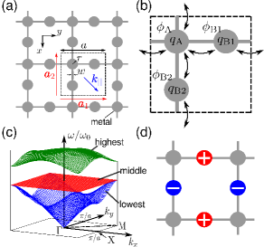
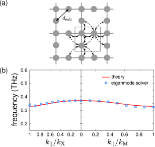
Using a model similar to the one in our previous study Nakata et al. (2012b), we derive the dispersion relation for spoof plasmons in the Lieb-type bar-disk resonators (LBDRs), as shown in Fig. 1(a). The lattice formed by the disks connected to four disks is named the main lattice, and the lattice formed by the disks connected to two disks is named the sublattice. We assume that the structure is made of an infinitely thin, lossless metal and the electric charge is stored only on each disk and oscillates alternately. The electric potential of the th disk can be expressed with the electric charge on the th disk as follows:
| (1) |
We only consider the self- and nearest-neighbor capacitive couplings, as shown in Fig. 1(b). The constants and are the potential coefficients, and is an adjacency matrix of the lattice; i.e., if the th and th disks are connected directly by a bar and otherwise . Using the wave vector on the plane of the LBDRs and the unit-lattice vectors and shown in Fig. 1(a), we can obtain the relation between the electric potentials and the electric charges of the three disks (A, B1, and B2) in the unit cell as follows:
| (4) |
where
| (8) |
with . We use tildes to represent complex amplitudes, and a harmonic time dependence with angular frequency is assumed.
Next, we introduce the current flowing from the th disk to the th disk and the self-inductance of the bar connecting the th and th disks. Then we have
| (9) |
From Eq. (9) and the charge conservation law at the th disk, we obtain
| (10) |
For the LBDRs, Eq. (10) is reduced to
| (13) |
in the frequency domain. The matrix is defined as follows:
| (17) |
Equations (4) and (13) give the following eigenvalue equation:
| (20) |
where and . Solving Eq. (20), we finally derive the dispersion relations
| (21) |
where . From these equations, we obtain the two-dimensional band structure shown in Fig. 1(c) for . Note that corresponds to neglecting the nearest neighbor capacitive couplings between the disks, but the disks are sufficiently coupled through currents flowing in the bars. There are three bands, and the middle band at is flat. Although usual tight-binding models with the same on-site potential present the degeneracy of a flat band and one Dirac cone at the point, only the lowest band touches the flat band at the point in Fig. 1(c). This is caused by on-site potential difference on the main lattice and sublattice for spoof plasmons on the Lieb lattice. From Eqs. (1) and (10) with , we have
| (22) |
where is the number of bars connected to the th disk. In Eq. (22), the first term and the second term represent hopping and on-site potential, respectively. We can see that on-site potentials on the main lattice and sublattice are actually different in Eq. (22). In this study, we focus our attention on the flat band.
The flat bands are formed by the localized modes with the charge distribution shown in Fig. 1(d). In the flat-band mode, the charges oscillate in antiphase on the sublattice and no charges are induced on the main lattice owing to destructive interference. Hence, spoof plasmons in the flat band are two-dimensionally confined.
III Simulation
To confirm the result of the previous theoretical calculation, we numerically simulate the electromagnetic response of the LBDRs. We use a commercial finite-element method solver (Ansys HFSS). The design parameters of the LBDRs in Fig. 1(a) are as follows: the length of the unit cell is , the bar width is , and the disk radius is . In our simulation, the LBDRs are made of infinitely thin, perfect electric conductors. To observe the flat band both in the radiative region and in the nonradiative region, we treat two cases: free-space transmission and attenuated total reflection (ATR) configurations Maier (2007). The transmission and ATR spectra, respectively, reflect the band structure of the LBDRs in the radiative and nonradiative regions.
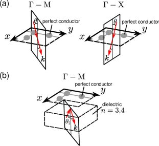
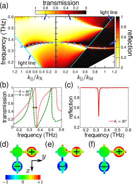
Figure 2(a) shows the setup of the transmission simulation. A plane wave enters into the LBDRs at an incident angle , which is varied from to . In this case, the magnitude of the wave vector on the sample plane is given by , where is the speed of light in vacuum. In order to excite the flat band mode, the incident wave is in the transverse electric (TE) mode for the – scan, and the transverse magnetic (TM) mode for the – scan.
Figure 2(b) shows the setup of the ATR simulation. The distance between the LBDRs and the dielectric is set to to reduce the proximity effect of the dielectric, as described in Sec V. A plane wave enters from the dielectric, which has refractive index , into the air. If the incident angle is larger than the critical angle , the incident wave is totally reflected, generating evanescent waves in the air. The refractive index of the dielectric is set to , assuming the use of silicon in the THz region Grischkowsky et al. (1990). The incident angle is varied from to , all of which are greater than . In this case, the magnitude of the wave vector on the sample plane is given by . The incident wave is in the TE mode for the – scan. The nonradiative region is negligibly small in the 1st Brillouin zone along the – line, so the ATR simulation is performed only in the – line.
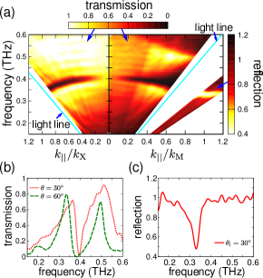
By using periodic boundary conditions with phase shifts, the transmission, reflection, and surface electric charge distribution in the unit cell are calculated for various incident angles. Figure 3(a) displays the simulation results of the transmission and ATR spectra in the wave-vector–frequency plane. We can observe a narrow band insensitive to the wave vector in the nonradiative region. We also observe a broader band in the radiative region from to .
To find where the flat band is located exactly, we use the eigenmode solver of HFSS, which provides the field distributions of resonant modes and their resonant frequencies for given structures and environments. In this simulation, we use periodic boundary conditions and the perfectly matched layer (PML). The PML regions are about half-wavelength apart from the LBDRs. In this configuration, the solver calculates the resonant mode propagating along the surface. The calculated eigenfrequencies are indicated by the open circles in Fig. 3(a). The charge distribution of this eigenmode corresponds to the flat-band mode illustrated in Fig. 1(d); therefore, we find that the narrow band in the nonradiative region is the flat band. On the other hand, the flat band in the radiative region is embedded in the high-transmission regions that are broadly distributed around to and is located on the boundary between the high- and low- transmission regions around . It is revealed that the flat band is bending, and the degree of the bend is about of the bottom frequency of the flat band along the – line, and along the – line. The reason for the bend is discussed in Sec. V.
Figure 3(b) shows the transmission spectra at incident angles and in the – scan, and Fig. 3(c) shows the ATR spectrum at an incident angle in the – scan. The ATR spectrum is simpler than the transmission spectra. For the transmission spectra, it is presumed that the flat-band mode interferes with the broad mode, as is the case in Fano interference Fano (1961).
Figures 3(d) and 3(e) show the surface electric charge distributions in the transmission configuration at the resonant frequencies: 0.362 THz for and 0.338 THz for in the – scan. Figure 3(f) shows the surface electric charge distributions of the ATR configuration at the resonant frequency 0.322 THz for in the – scan. It is clear that the surface charge oscillates in antiphase on the two disks of the sublattice in the unit cell. This resonant mode coincides with the theoretical charge distribution of the flat-band mode described in Sec. II. Therefore, we can conclude that the flat band is observed.
We also calculate the group velocity and the quality factor of the flat-band mode in the nonradiative region from the eigenfrequencies obtained by the eigenmode solver along the – line. The group velocity is obtained from the slope of the straight line fitted to the eigenfrequencies in the nonradiative region. In our simulation, we obtain the quality factor in the nonradiative region, which is a factor of 350 higher than the quality factor in the radiative region.
IV Experiments
IV.1 Experimental setup
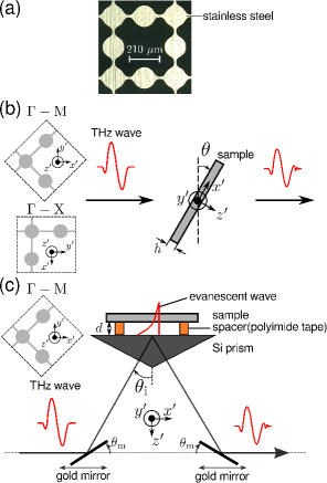
Figure 4(a) shows the LBDRs patterned on a stainless-steel (SUS304) sheet with thickness by etching. The period of the lattice is and the whole area is . To observe the dispersion relation in the radiative and nonradiative regions experimentally, we perform a transmission measurement using THz time-domain spectroscopy (THz-TDS), as shown in Fig. 4(b) Nakata et al. (2012b), and a total reflection measurement using THz time-domain attenuated total reflection (TD-ATR) spectroscopy, as shown in Fig. 4(c) Hirori et al. (2004). We use a THz emitter and detector (EKSPLA, Ltd.) with dipole antennas. The antennas are fixed on low-temperature-grown GaAs photoconductors illuminated by a femtosecond fiber laser (F-100, IMRA America, Inc.) with a wavelength of and pulse duration of . A silicon lens is used to produce a collimated THz beam with diameter of . The electric field of the THz wave, is measured in the time domain. In the TD-ATR measurement, a silicon prism Grischkowsky et al. (1990) with refractive index is used. The distance between the LBDRs and the prism is (the thickness of the polyimide spacing tape). We can obtain the transmission spectrum and the ATR spectrum from and , where and are the Fourier-transformed electric fields with and without the sample, respectively.
To observe the band structure experimentally, the incident angle is changed in each measurement as follows: (a) In the transmission measurement, the sample is rotated by around the axis from normal incidence, as shown in Fig. 4(b). The incident angle is changed from to in steps of , and the corresponding wave number is given by . The incident wave is in the TE mode for the – scan, and the TM mode for the – scan. (b) In the total reflection measurement, the gold mirrors are rotated from to by , corresponding to changing the incident angle from to , as shown in Fig. 4(c). The incident wave is in the TE mode. The angle, or in-plane wave vector, is limited by the finite size of the mirror mounts and the finite area of the LBDRs. The corresponding wave number is given by .
IV.2 Results
Figure 5 displays the results of the experiments. The transmission and ATR spectra mapped on the wave-vector–frequency plane are shown in Fig. 5(a). In the nonradiative region, a single ATR dip that is insensitive to the wave number is observed. In the radiative region, there exists a broader band from to . These results are qualitatively and almost quantitatively in good agreement with the simulation shown in Fig. 3(a). Figure 5(b) shows the transmission spectra at the incident angles and in the – scan. Figure 5(c) shows the ATR spectrum at the incident angle in the – scan. These results also agree well with the results of the simulation.
Compared with the simulation result obtained for ideal conditions, the resonant frequency of the flat-band mode is a little higher, and the line width of the spectrum broadens. The possible reasons for these disagreements are as follows: First, although the LBDRs are assumed to be perfect conductors in the simulation, the fabricated LBDRs used in the experiment have the finite conductivity of the stainless steel. It has been confirmed that the line width of the spectrum broadens also in the simulation for the LBDRs with finite conductivity (see Sec. V). Second, owing to the lack of precision of the etching, the width of the bar is widened. This causes a decrease of the effective inductance of the bar, and the resonant frequency shifts higher. Finally, the distance between the LBDRs and the prism, in the experiment differs from the simulation parameter . The dependence of the ATR spectra on the distance between the LBDRs and the prism is discussed in Sec. V.
V Discussion
V.1 Origin of the bend of the flat band
The flat-band frequency is slightly dependent on the wave vector both in the simulation and in the experiment. As a major cause we consider the second-nearest-neighbor capacitive couplings, as shown in Fig. 6(a), in addition to the nearest-neighbor couplings. In this model, Eq. (1) is replaced with
| (23) |
We define the distance between the centers of the two disks of the sublattice in a unit cell as . if the th disk exists within a radius from the center of the th disk; otherwise .
By using Eq. (23) instead of Eq. (1), in Eq. (4) is replaced with
| (27) |
where . The dispersion relation is obtained by solving the eigenvalue problem .
The solid line in Fig. 6(b) is the theoretical curve fitted to the eigenfrequencies (shown as open circles) that are obtained by the eigenmode solver. By solving the eigenvalue problem of , we obtain the frequencies of the flat-band mode at the point as , the point as , and the point as . By averaging of the eigenfrequencies and at the and points, the parameter is determined. From the eigenfrequency at the point, the parameter is determined. We note that the variation of the curve is affected only by the parameter , not by . This is because the second-nearest-neighbor couplings break the condition on the formation of the localized modes. For simplification, we assume the value of as . If , the band takes its minimal value at ; in contrast, if , it takes its maximal value. In the static limit (), positive charges on a disk create positive electric potential on the other disks; hence the parameter is expected to be positive. However, the actual value of is negative. This can be explained by the retardation effect Liu et al. (2012); Tatartschuk et al. (2012). The phase difference between the second-nearest disks is given by at . The negative sign of is caused by this shift being greater than . Note that the second-nearest-neighbor coupling is weakened by reducing the disk radius and the bar width without changing the length of the unit cell, and we could further suppress the degree of the bend by improving the precision of the fabrication.
V.2 Dependence of ATR spectra on the distance between the LBDRs and the prism
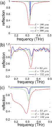
The flat band in the nonradiative region cannot couple with free-space modes; theoretically, this mode has no energy radiation into free space and is perfectly confined at the surface. However, in our situation, the nonradiative flat-band mode is excited by evanescent waves. The evanescent waves are generated by the total reflection of the propagating waves; that is, the flat-band mode couples with the propagating waves. This coupling strength depends on the distance between the LBDRs and the prism. It is expected that the width of the ATR dip becomes narrower by increasing the distance because the coupling strength is weakened.
To verify the coupling effect, we perform total reflection measurements with several distances in the simulation and the experiment. The simulation is performed for , 200, and under the same conditions of the ATR configuration in Sec. III. In the experiment, the distance is changed by increasing the number of polyimide spacer layers from one to three. Figures 7(a) and 7(b) show the results of the simulation and the experiment, respectively. These results demonstrate that the ATR dip becomes narrower and shallower as increases. Furthermore, we see that, as the distance between the LBDRs and the prism is increased, the resonant frequency shifts to higher frequency and converges to the resonant frequency in free space. Figure 7(c) shows the ATR spectra obtained by the simulation in the case where the finite-conductivity boundary condition with the DC conductivity of SUS304 is applied to the infinitely thin LBDRs region Davis (1998). From this result, we can confirm that the spectra are broadened owing to the finite conductivity in the ATR experiment.
VI Conclusion
In this paper, we demonstrated the three-dimensionally confined flat-band mode for spoof surface plasmons. We analytically calculated the dispersion relation of spoof plasmons on the LBDRs based on the electrical circuit model. We obtained three bands, the middle of which is a flat band. To confirm this theoretical result, we numerically simulated the electromagnetic response of the LBDRs using the finite-element method. The simulation results revealed that the flat band in the nonradiative region shows narrower line width than that in the radiative region. Besides, we found that the flat-band bend can be explained by the second-nearest-neighbor capacitive coupling. Finally, we performed transmission and total reflection measurements using the THz-TDS and the TD-ATR methods. The experimental results showed qualitatively good agreement with the simulation results.
In the total reflection measurement, as the distance between the sample and the coupling prism is increased, the coupling strength between the spoof surface plasmons and the evanescent wave is weakened, and the ATR dip becomes narrower. Because spatially localized modes can be formed, these modes can be applied to sensitive plasmon sensors Yoshida et al. (2007) with high spatial resolution. Furthermore, combined with the low group velocity, the flat-band mode with a high quality factor can be used to enhance the nonlinear response of materials Tamayama et al. (2015).
Acknowledgements.
We gratefully thank Dr. Atsushi Yao and Professor Takashi Hikihara for allowing us to use their equipment and Professor Fumiaki Miyamaru for fruitful discussions. The present research is supported by JSPS KAKENHI Grants No. 22109004, No. 25790065, and No. 25287101.References
- Maier (2007) S. A. Maier, Plasmonics: fundamentals and applications (Springer Science & Business Media, New York, 2007).
- Maier et al. (2006) S. A. Maier, S. R. Andrews, L. Martin-Moreno, and F. J. Garcia-Vidal, Phys. Rev. Lett. 97, 176805 (2006) .
- Williams et al. (2008) C. R. Williams, S. R. Andrews, S. Maier, A. Fernández-Domínguez, L. Martín-Moreno, and F. Garcia-Vidal, Nature Photon. 2, 175 (2008) .
- Pendry et al. (2004) J. B. Pendry, L. Martin-Moreno, and F. J. Garcia-Vidal, Science 305, 847 (2004) .
- Fernndez-Domínguez et al. (2008) A. I. Fernndez-Domínguez, L. Martín-Moreno, F. J. García-Vidal, S. R. Andrews, and S. A. Maier, IEEE J. Sel. Topics in Quantum Electron. 14, 1515 (2008) .
- Gan et al. (2008) Q. Gan, Z. Fu, Y. J. Ding, and F. J. Bartoli, Phys. Rev. Lett. 100, 256803 (2008) .
- Yu et al. (2010) N. Yu, Q. J. Wang, M. A. Kats, J. A. Fan, S. P. Khanna, L. Li, A. G. Davies, E. H. Linfield, and F. Capasso, Nature Mater. 9, 730 (2010) .
- Lieb (1989) E. H. Lieb, Phys. Rev. Lett. 62, 1201 (1989) .
- Tasaki (1992) H. Tasaki, Phys. Rev. Lett. 69, 1608 (1992) .
- Mielke (1991) A. Mielke, J. Phys. A Math Gen. 24, 3311 (1991) .
- Takeda et al. (2004) H. Takeda, T. Takashima, and K. Yoshino, J. Phys. Condens. Matter 16, 6317 (2004) .
- Vicencio et al. (2015) R. A. Vicencio, C. Cantillano, L. Morales-Inostroza, B. Real, C. Mejía-Cortés, S. Weimann, A. Szameit, and M. I. Molina, Phys. Rev. Lett. 114, 245503 (2015) .
- Mukherjee et al. (2015) S. Mukherjee, A. Spracklen, D. Choudhury, N. Goldman, P. Öhberg, E. Andersson, and R. R. Thomson, Phys. Rev. Lett. 114, 245504 (2015) .
- Endo et al. (2010) S. Endo, T. Oka, and H. Aoki, Phys. Rev. B 81, 113104 (2010) .
- Feigenbaum and Atwater (2010) E. Feigenbaum and H. A. Atwater, Phys. Rev. Lett. 104, 147402 (2010) .
- Nakata et al. (2012a) Y. Nakata, T. Okada, T. Nakanishi, and M. Kitano, Phys. Status Solidi (b) 249, 2293 (2012a) .
- Nakata et al. (2012b) Y. Nakata, T. Okada, T. Nakanishi, and M. Kitano, Phys. Rev. B 85, 205128 (2012b) .
- Grischkowsky et al. (1990) D. Grischkowsky, S. Keiding, M. Van Exter, and C. Fattinger, J. Opt. Soc. Am. B 7, 2006 (1990) .
- Fano (1961) U. Fano, Phys. Rev. 124, 1866 (1961) .
- Hirori et al. (2004) H. Hirori, K. Yamashita, M. Nagai, and K. Tanaka, Jpn. J. Appl. Phys. 43, L1287 (2004) .
- Liu et al. (2012) M. Liu, D. A. Powell, I. V. Shadrivov, and Y. S. Kivshar, Appl. Phys. Lett. 100, 111114 (2012) .
- Tatartschuk et al. (2012) E. Tatartschuk, N. Gneiding, F. Hesmer, A. Radkovskaya, and E. Shamonina, J. Appl. Phys. 111, 094904 (2012) .
- Davis (1998) J. R. Davis, Metals handbook (ASM international, Materials Park, OH, 1998).
- Yoshida et al. (2007) H. Yoshida, Y. Ogawa, Y. Kawai, S. Hayashi, A. Hayashi, C. Otani, E. Kato, F. Miyamaru, and K. Kawase, Applied physics letters 91, 253901 (2007) .
- Tamayama et al. (2015) Y. Tamayama, K. Hamada, and K. Yasui, Phys. Rev. B 92, 125124 (2015) .