Topological insulator homojunctions including magnetic layers: the example of n-p type (-QLs Bi2Se3/Mn-Bi2Se3) heterostructures
Abstract
Homojunctions between Bi2Se3 and its Mn-doped phase are investigated as a sample geometry to study the influence of spin degrees of freedom on topological insulator properties. quintuple layers (QLs) of Bi2Se3 are grown ontop of Mn-doped Bi2Se3 by molecular beam epitaxy for QLs, allowing to unhamperedly monitor the development of electronic and topological properties by surface sensitive techniques like angle resolved photoemission spectroscopy. With increasing , a Mn-induced gap at the Dirac point is gradually filled in an ”hourglass” fashion to reestablish a topological surface state at QLs. Our results suggest a competition of upwards and downwards band bending effects due to the presence of an n-p type interface, which can be used to tailor topological and quantum well states independently.
The material class of topological insulators (TIs) is presently in the focus of research, due to its fascinating fundamental physics but also its potential for future spintronic applications Hasan and Kane (2010); Qi and Zhang (2011). Experimentally, the TI phase was first observed in 2D HgTe/HgCdTe quantum well systems, possessing spin-polarised helical 1D edge states König et al. (2007); Bernevig, Hughes, and Zhang (2006). Later, chalcogenide-type materials like Bi2Te3 and Bi2Se3 with large spin-orbit coupling were shown to host 2D topological surface states (TSSs), defined by a Dirac-like dispersion, which locks momentum solutions and to opposite spin Pesin and MacDonald (2012).
The intimate link between time reversal symmetry and TI properties soon raised the fundamental question how magnetic degrees of freedom influence TI properties. Stable local moments with perpendicular to the surface should break time reversal symmetry and are predicted to cause an energy gap at the Dirac point (DP) Liu et al. (2009); Henk et al. (2012).
Strategies to couple magnetic moments to the TSS are so far devided into surface concepts (magnetic adatoms) and bulk strategies (magnetic dopants). Surface concepts included adsorbed magnetic single atoms Honolka et al. (2012); Scholz et al. (2012); Eelbo et al. (2014); Sessi et al. (2014) and superparamagnetic clusters Wray et al. (2011). The disadvantage of surface approaches are the lack of stable moments in the impurity limit (fluctuating moments with ) and the obstructed access to the TSS at larger coverages by experimental techniques such as surface sensitive angle-resolved photoelectron spectroscopy (ARPES). Bulk strategies promise larger potential since a stable ferromagnetic phase can be induced within the TI bulk material itself, potentially influencing the TSSs within their decay length into the bulk over several nanometers Song et al. (2010). For chalcogenide based materials theory predicts several possible magnetic interaction mechanisms (Biswas and Balatsky, 2010; Abanin and Pesin, 2011; Efimkin and Galitski, 2014; Choi et al., 2012) and ferromagnetic ordering was reported e.g. for 3 elements Fe, Mn, and Cr in bulk Bi2Te3 or Bi2Se3 samples Xu and et al (2012); Zhang et al. (2012); von Bardeleben et al. (2013) with Curie temperatures ranging from K to K.
Although bulk concepts are vividly studied, reports on the influence of ferromagnetic bulk phases on TSSs are contradictive and controversively dicussed Xu and et al (2012); Růžička et al. (2015). Moreover, assignments to existing theory on magnetic ordering is difficult, since 3 atoms tend to integrate into the host matrix in various ways, strongly depending on sample preparation parameters.
In this work, we follow a different approach based on layered Bi2Se3 heterostructures with a buried magnetic phase. Using molecular beam epitaxy (MBE), an increasing number of pure Bi2Se3 quintuple layers (QLs) is grown ontop of Mn-doped Bi2Se3. ARPES and X-ray photoelectron spectroscopy (XPS) were done in Aarhus at the synchrotron ASTRID 2 Hoffmann et al. (2004) and in Prague using an Omicron NanoESCA instrument with laboratory light sources. Our band structure data suggest a gradual decoupling of the Bi2Se3 TSS from influences of the buried magnetic phase, and non-monotoneous band bending (BB) profiles caused by the proximity of the n-p type interface with Mn-doped Bi2Se3. Our results stress the potential of such systems to study time reversal symmetry breaking influences on TSSs under well-defined pertubative conditions exploiting band engineering strategies.
Bi2Se3-based systems were epitaxially grown on insulating BaF2(111)
and the structural order of the material was monitored by reflection high energy electron diffraction (RHEED). Since the (0001) basal plane of the trigonal Bi2Se3 lattice is nearly lattice-matched to BaF2(111), two-dimensional layer growth with good crystalline quality can be obtained. For details on the growth procedure see Ref. Caha et al. (2013).
Mn-doped Bi2Se3 thin films of different thickness were grown at C under Se-rich conditions to support 3d substitutional implementation with respect to e.g. interstitial defects Song et al. (2010). Additional quintuple layers of pure Bi2Se3 were grown continuously ontop the Mn-doped phase at slightly lower temperatures C to form -QLs Bi2Se3/Mn-Bi2Se3 heterostructures. In this work data of two sample series () and () on respective Mn-doped Bi2Se3 films of 500nm and 300nm thickness are shown.
The epitaxial heterostructures were finally protected against oxidation by amorphous Se cap layers, which allows to recover large, atomically flat terraces by an in-situ decapping procedure under ultra-high vacuum conditions (see detailed information supplementary, Fig. S1). Se desorption was monitored by mass spectrometry, and successful decapping was verified in Se and Bi XPS core level (CL) data for each sample shown in this work.
From bulk sensitive energy dispersive X-ray spectroscopy (EDX) maps with a lateral resolution of about 1m we can exclude significant variations of the Mn concentration or crystal precipitations on this length scale and beyond. Estimations of Bi, Se, and Mn concentrations are summarized in Table 1 for two sample series and , respectively. Comparing the stoichiometry of films with and without Mn, we find that the Bi/Se ratio 2/3 is not significantly altered by Mn implementation. At Mn concentrations we find Curie temperatures of about 5K in SQUID measurements. Bulk sensitive X-ray diffraction studies,
moreover, prove a high degree of order in the film. For details we refer the reader to our separate work focused on bulk properties Tarasenko et al. (2016).
| [%] | [%] | [K] | |||
|---|---|---|---|---|---|
| Series (nm) | 36.6 | 51.3 | 0.71 | 12.1 | 5.4 |
| Series (nm) | 34.6 | 51.1 | 0.68 | 13.8 | 5.2 |
| Melt-grown Bi2Se3 | 40.5 | 59.5 | 0.68 | 0 | – |
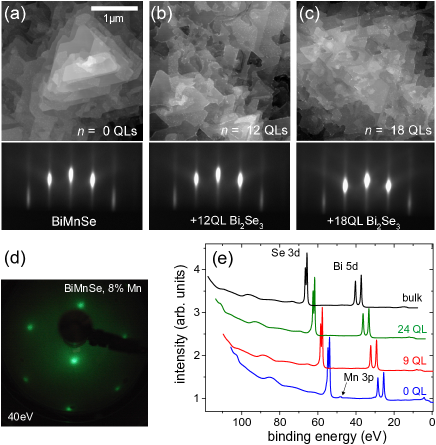
Fig. 1 summarizes the overgrowth properties of (-QLs Bi2Se3/Mn-Bi2Se3) heterostructures with different number of QLs. AFM images (a)-(c) at and show material-typical pyramidal growth during MBE.
We find that the height corrugation at and is similar to the homogeneous phase with , and triangular terraces show mirrored geometries typical for twinning in chalcogenide TIs under the influence of 3 metal dopants. In addition, the average terrace width is reduced compared to pure MBE-grown Bi2Se3.
The corresponding RHEED patterns do not significantly change with , indicating that despite the increased corrugation, the crystal growth conditions do not change dramatically at the interface between Mn-doped and undoped Bi2Se3. LEED images in Fig. 1(d) and XPS Se 3 and Bi 5 core level spectra shown in (e) confirm well-defined (111)-oriented and chemically ordered surfaces after decapping.
Highly-resolved XPS allows to detect chemical shifts in Mn, Bi and Se CLs, which depend on the atom‘s chemical environments within the XPS sampling depth .
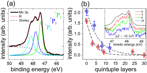
First we are interested in the electronic ground state of Mn dopants itself. The Mn 3 core level spectrum in Fig. 2(a) for exhibits a sharp multiplet structure, suggesting a well defined Mn electronic configuration in the Bi2Se3 host. This is in contrast to a metallic Mn phases where a broad almost featureless 3 spectrum is observed at same photon energies due to solid state broadening Noh et al. (2015); von dem Borne et al. (2000). The comparison proves that Mn atoms are not significantly clustered in our samples. Instead, the spectrum can be perfectly described by a (, , ) multiplet of a Mn ground state, which under the influence of core hole interactions splits in binding energy (BE) with the according intensities (see Fig. 2(a)). The width of the three Voigt components increases with BE, as expected from increasing super-Coster-Kronig decay processes caused by the large overlap of the Mn 3 with the 3 wavefunctions Martins et al. (2006). For a direct comparison of the line shape evolution with , the inset of Fig. 2(b) presents the scaled Mn 3 signals, which shows that the width of the Mn multiplet does not change significantly. As we will discuss in more detail below, the gradual and rigid shifts of the triplet structure by up to eV towards higher kinetic energies suggests upwards band bending (UBB) effects within the probed buried Mn-doped Bi2Se3 phase with inreasing .
The XPS probing depth can be directly estimated from the Mn XPS peak intensities of sample series and for photon energies eV and eV, respectively, as summarized in Fig. 2(b). Mn 2 and 3 intensities decay approximately exponentially with increasing and the fits using Lambert-Beer’s law correspond to effective electron mean free paths nm and nm. is expected due to higher kinetic energy of electrons excited with eV. The value is larger than expected for the given kinetic energy.
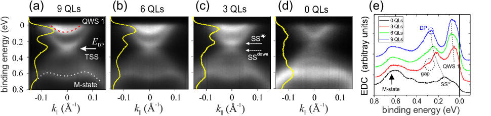
The heterostructure geometry allows the unobstructed study of the TSS under the influence of the buried magnetic phase. Fig. 3(a)-(d) summarizes the ARPES spectra of the sample series measured at K and and photon energy eV. We stress that precise cuts through the point were extracted from data sets covering the full Fermi surface range.
The ARPES cuts along reveal clear trends with decreasing .
Starting from large numbers of QLs, at a typical n-doped Bi2Se3 TSS is observed in Fig. 3(a) with a DP located at eV. In addition, a parabolic band is visible close to and M-shaped states dominate at eV. Both are well-known features for n-doped Bi2Se3, originating from conduction and valence band states, respectively Bianchi et al. (2011). Fig. 4 proves that in our case the parabolic states close to do not disperse with photon energy, typical for 2D quantum well states (QWS) formed in a near-surface downwards band bending (DBB) potential.
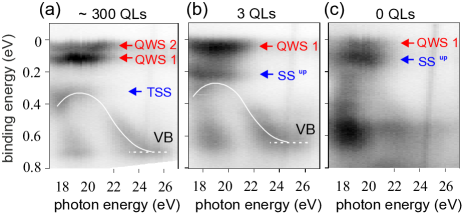
Reducing the number of QLs, the TSS gradually becomes massive forming a gap at the DP, limited at the top and bottom by the bands SS and SS as indicated in Fig. 3(c). We emphasize that ARPES was done in the paramagnetic phase . Fig. 4(b) shows that SS does not disperse with photon energy and thus inherits the TSS‘s 2D nature as expected. Finally, Fig. 3(d) shows that for , disctinct resonances appear in a seemingly increased gap between the M-state and SS.
Trends of intensity around the point are best visible in energy distribution curves (EDCs) averaged in the range [, ], which are plotted in the respective ARPES images and for direct comparison in Fig. 3(e). Starting as an intact TSS at , a gap at manifests itself as a dip at in the EDC, best visible for .
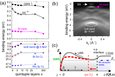
The development of SS, QWS 1 and M-state with are shown in the top panel of Fig. 5(a).
SS shifts up towards lower BEs by more than eV between and , while QWS and M-state shift by less than eV.
The parallel development of QWS and M-states with suggests subtle changes of near-surface DBB, similar to those induced e.g. by adsorbates on bulk Bi2Se3 Bianchi et al. (2012). In contrast, the much stronger shift of SS in the range QLs proves an independent development for states of topological origin, e.g. due to subsurface Mn impurities creating a gap and introducing resonances around the DP Black-Schaffer and Balatsky (2012) as observed in our ARPES data. We briefly mention that below QLs the overlap of degenerate front and backside TSS wavefunctions in free standing Bi2Se3 films should create a gap Park (2015), however, this effect can be disabled due to the Mn-doped Bi2Se3 interface, which induces onesided energy shifts Eremeev et al. (2015).
The interpretation of our data is complicated by the fact that in contrast to SSs and QWSs, CLs in XPS move to lower BEs with as discussed above for Mn 3, and observed much more distinctively for Bi 5 and Se CLs in both sample series and (see Fig. 5(a), bottom panel and Supplementary Fig. S2). For a better understanding we measured ARPES up to BEs of eV as shown in Fig. 5(b). A characteristic Bi2Se3 bulk band maximum at BE eV is visible Zhang et al. (2010), which shifts strictly parallel to the localized Bi and Se CLs with increasing (see Fig. 5(a), lower panel), suggesting UBB in a surface volume according to our probing depth 3-4 QLs.
UBB effects of meV on length scales larger than 3-4 QLs have indeed been predicted for heavily and intermediately n-doped Bi2Se3 Veyrat et al. (2015); Förster, Krüger, and Rohlfing (2015) in the absence of surface doping as a consequence of bulk charge transfer from donor states (e.g. Se-vacancy states) into available SSs. For our heterostrucures we seem to be able to tune this effect by the parameter . From the fact that Mn CL shifts are considerably smaller, we infer that BB happens mostly in the Bi2Se3 overlayers. Taking the shifts of all states into account we propose that near-surface DBB only affect QWS in a very small subsurface range ,
while UBB governs deeper layers as shown in the conduction BB schemes in Fig. 5(c) for the cases and QLs. Such a band bending model is supported by recent theoretical predictions Park, Beule, and Partoens (2013). This model, which assumes Mn to create midgap or shallow p-type levels Zhang et al. (2014); Choi et al. (2012)
and thus a p-n-interface with Bi2Se3 overlayers, qualitatively explains both the independent spectroscopic trends of QW, surface, and bulk electron states, as well as the different degrees of UBB effects observed in buried Mn and overlayer Bi/Se CLs.
In summary, we studied MBE-grown layered Bi2Se3 heterostructures with a buried Mn-doped phase.
The geometry of quintuple layers (QLs) Bi2Se3 ontop of Mn-doped Bi2Se3 allows to unhamperedly monitor the development of surface electronic properties, which reveals a gradual recovery of a gapped topological surface state with increasing , but also strong band bending effects due to the surface proximity of the heterostructure interface. Our results stress the potential of such sample geometries as a model system to study magnetic influences on topological insulator phases under well-defined pertubative conditions with the option to exploit band engineering techniques.
Acknowledgements.
The authors acknowledge financial support from the Czech Science Foundation (Grant P204/14/30062S), CALIPSO, the DFG under SPP1666, Villum fonden and the Aarhus University Research foundation. J.H. acknowleges the Purkyně Fellowship of the ASCR.References
- Hasan and Kane (2010) M. Z. Hasan and C. L. Kane, Rev. Mod. Phys. 82, 3045 (2010).
- Qi and Zhang (2011) X.-L. Qi and S.-C. Zhang, Rev. Mod. Phys. 83, 1057 (2011).
- König et al. (2007) M. König, S. Wiedmann, C. Brüne, A. Roth, H. Buhmann, L. W. Molenkamp, X.-L. Qi, and S.-C. Zhang, Science 318, 766 (2007).
- Bernevig, Hughes, and Zhang (2006) B. A. Bernevig, T. L. Hughes, and S.-C. Zhang, Science 314, 1757 (2006).
- Pesin and MacDonald (2012) D. Pesin and A. H. MacDonald, Nature Materials 11, 409 (2012).
- Liu et al. (2009) Q. Liu, C.-X. Liu, C. Xu, X.-L. Qi, and S.-C. Zhang, Phys. Rev. Lett. 102, 156603 (2009).
- Henk et al. (2012) J. Henk, M. Flieger, I. V. Maznichenko, I. Mertig, A. Ernst, S. V. Eremeev, and E. V. Chulkov, Phys. Rev. Lett. 109, 076801 (2012).
- Honolka et al. (2012) J. Honolka, A. A. Khajetoorians, V. Sessi, T. O. Wehling, S. Stepanow, J.-L. Mi, B. B. Iversen, T. Schlenk, J. Wiebe, N. B. Brookes, A. I. Lichtenstein, P. Hofmann, K. Kern, and R. Wiesendanger, Phys. Rev. Lett. 108, 256811 (2012).
- Scholz et al. (2012) M. R. Scholz, J. Sánchez-Barriga, D. Marchenko, A. Varykhalov, A. Volykhov, L. V. Yashina, and O. Rader, Phys. Rev. Lett. 108, 256810 (2012).
- Eelbo et al. (2014) T. Eelbo, M. Waśniowska, M. Sikora, M. Dobrzański, A. Kozłowski, A. Pulkin, G. Autès, I. Miotkowski, O. V. Yazyev, and R. Wiesendanger, Phys. Rev. B 89, 104424 (2014).
- Sessi et al. (2014) P. Sessi, F. Reis, B. Thomas, K. A. Kokh, O. E. Tereshchenko, and M. Bode, Nature Communications 5, 5349 (2014).
- Wray et al. (2011) L. A. Wray, S.-Y. Xu, Y. Xia, D. Hsieh, A. V. Fedorov, Y. S. Hor, R. J. Cava, A. Bansil, H. Lin, and M. Z. Hasan, Nat Phys 7, 32 (2011).
- Song et al. (2010) C.-L. Song, Y.-L. Wang, Y.-P. Jiang, Y. Zhang, C.-Z. Chang, L. Wang, K. He, X. Chen, J.-F. Jia, Y. Wang, Z. Fang, X. Dai, X.-C. Xie, X.-L. Qi, S.-C. Zhang, Q.-K. Xue, and X. Ma, Applied Physics Letters 97, 143118 (2010).
- Biswas and Balatsky (2010) R. R. Biswas and A. V. Balatsky, Phys. Rev. B 81, 233405 (2010).
- Abanin and Pesin (2011) D. A. Abanin and D. A. Pesin, Phys. Rev. Lett. 106, 136802 (2011).
- Efimkin and Galitski (2014) D. K. Efimkin and V. Galitski, Phys. Rev. B 89, 115431 (2014).
- Choi et al. (2012) Y. H. Choi, N. H. Jo, K. J. Lee, H. W. Lee, Y. H. Jo, J. Kajino, T. Takabatake, K.-T. Ko, J.-H. Park, and M. H. Jung, Applied Physics Letters 101, 152103 (2012).
- Xu and et al (2012) S.-Y. Xu and et al, Nature Physics 8, 616 (2012).
- Zhang et al. (2012) J.-M. Zhang, W. Zhu, Y. Zhang, D. Xiao, and Y. Yao, Phys. Rev. Lett. 109, 266405 (2012).
- von Bardeleben et al. (2013) H. J. von Bardeleben, J. L. Cantin, D. M. Zhang, A. Richardella, D. W. Rench, N. Samarth, and J. A. Borchers, Phys. Rev. B 88, 075149 (2013).
- Růžička et al. (2015) J. Růžička, O. Caha, V. Holý, H. Steiner, V. Volobuiev, A. Ney, G. Bauer, T. Duchoň, K. Veltruská, I. Khalakhan, V. Matolín, E. F. Schwier, H. Iwasawa, K. Shimada, and G. Springholz, New Journal of Physics 17, 013028 (2015).
- Hoffmann et al. (2004) S. V. Hoffmann, C. Søndergaard, C. Schultz, Z. Li, and P. Hofmann, Nuclear Instruments and Methods in Physics Research, A 523, 441 (2004).
- Caha et al. (2013) O. Caha, A. Dubroka, J. Humlíček, V. Holý, H. Steiner, M. Ul-Hassan, J. Sánchez-Barriga, O. Rader, T. N. Stanislavchuk, A. A. Sirenko, G. Bauer, and G. Springholz, Crystal Growth & Design 13, 3365 (2013).
- Tarasenko et al. (2016) R. Tarasenko, M. Vališka, M. Vondráček, K. Horáková, V. Tkáč, K. Carva, P. Baláž, V. Holý, G. Springholz, V. Sechovský, and J. Honolka, Physica B: Condensed Matter 481, 262 (2016).
- Noh et al. (2015) H.-J. Noh, J. Jeong, E.-J. Cho, J. Park, J. S. Kim, I. Kim, B.-G. Park, and H.-D. Kim, Phys. Rev. B 91, 121110 (2015).
- von dem Borne et al. (2000) A. von dem Borne, R. L. Johnson, B. Sonntag, M. Talkenberg, A. Verweyen, P. Wernet, J. Schulz, K. Tiedtke, C. Gerth, B. Obst, P. Zimmermann, and J. E. Hansen, Phys. Rev. A 62, 052703 (2000).
- Martins et al. (2006) M. Martins, K. Godehusen, T. Richter, P. Wernet, and P. Zimmermann, Journal of Physics B: Atomic, Molecular and Optical Physics 39, R79 (2006).
- Bianchi et al. (2011) M. Bianchi, R. C. Hatch, J. Mi, B. B. Iversen, and P. Hofmann, Phys. Rev. Lett. 107, 086802 (2011).
- Bianchi et al. (2012) M. Bianchi, R. C. Hatch, D. Guan, T. Planke, J. Mi, B. B. Iversen, and P. Hofmann, Semiconductor Science and Technology 27, 124001 (2012).
- Black-Schaffer and Balatsky (2012) A. M. Black-Schaffer and A. V. Balatsky, Phys. Rev. B 86, 115433 (2012).
- Park (2015) B. C. Park, Nature Communications 6, 6552 (2015).
- Eremeev et al. (2015) S. Eremeev, V. Men׳shov, V. Tugushev, and E. Chulkov, Journal of Magnetism and Magnetic Materials 383, 30 (2015), selected papers from the sixth Moscow International Symposium on Magnetism (MISM-2014).
- Zhang et al. (2010) W. Zhang, R. Yu, H.-J. Zhang, X. Dai, and Z. Fang, New Journal of Physics 12, 065013 (2010).
- Veyrat et al. (2015) L. Veyrat, F. Iacovella, J. Dufouleur, C. Nowka, H. Funke, M. Yang, W. Escoffier, M. Goiran, B. Eichler, O. G. Schmidt, B. Büchner, S. Hampel, and R. Giraud, Nano Letters 15, 7503 (2015), pMID: 26479681.
- Förster, Krüger, and Rohlfing (2015) T. Förster, P. Krüger, and M. Rohlfing, Phys. Rev. B 91, 035313 (2015).
- Park, Beule, and Partoens (2013) K. Park, C. D. Beule, and B. Partoens, New Journal of Physics 15, 113031 (2013).
- Zhang et al. (2014) X. M. Zhang, G. Z. Xu, Y. Du, E. K. Liu, Z. Y. Liu, W. H. Wang, and G. H. Wu, Journal of Applied Physics 115, 083704 (2014).