Scanning gate imaging in confined geometries
Abstract
This article reports on tunable electron backscattering investigated with the biased tip of a scanning force microscope. Using a channel defined by a pair of Schottky gates, the branched electron flow of ballistic electrons injected from a quantum point contact is guided by potentials of a tunable height well below the Fermi energy. The transition from injection into an open two-dimensional electron gas to a strongly confined channel exhibits three experimentally distinct regimes: one in which branches spread unrestrictedly, one in which branches are confined but the background conductance is affected very little, and one where the branches have disappeared and the conductance is strongly modified. Classical trajectory-based simulations explain these regimes at the microscopic level. These experiments allow us to understand under which conditions branches observed in scanning gate experiments do or do not reflect the flow of electrons.
pacs:
73.23.AdWhoever has looked at twinkling starlight witnessed how atmospheric inhomogeneity randomly focuses light Lynch and Livingston (2001). The inhomogeneity consists of small, random, but spatially correlated fluctuations of the refractive index. This rather common phenomenon is only one out of many examples, in which small random potentials generate regions of exceedingly high flow density, a bunching of particle trajectories, also known as caustics Berry (1975). In two-dimensional systems caustics form pairs of lines with an appearance like the branches of a tree. Topinka and coworkers were the first to observe such branches at the nano-scale in high quality two-dimensional electron gases Topinka et al. (2001). In this system charged doping atoms randomly placed in a plane remote from the electron gas generate a smooth spatially correlated potential landscape. At liquid helium temperatures and below, the electrons emanating from a narrow constriction into this landscape exhibit branched flow Heller and Shaw (2003). Topinka observed it using the strongly repulsive electrostatic potential of a scanning tip to scatter channels of high flow density back through the constriction. Placing the tip along a caustic thereby measurably reduced the system’s conductance. A spatially resolved image of the branch pattern was obtained by mapping the conductance as a function of tip-position. The method, known as scanning gate microscopy Eriksson et al. (1996a), sparked hopes to observe other predicted phenomena of electron trajectories in nanostructured systems, such as wave function scars in ballistic stadiums. However, experimental success was very limited Crook et al. (2003); Burke et al. (2010); Ferry et al. (2011); Aoki et al. (2012). Theoretically it is straight forward to calculate a backscattering pattern from known wave functions. The other way round, to extract the pattern of wave functions from an experimentally observed branch pattern is difficult to impossible. Furthermore, scanning gate measurements are by definition intrusive experiments and the conclusion one can draw about unperturbed wave functions are limited. Imaging and understanding the evolution of branches and caustics in geometries tunable between free and confined electron motion therefore remains an interesting experimental challenge. Here we tackle the problem using a sample-geometry simple enough to interpret the resulting conductance maps conclusively. Our experiments lead to striking general insights into the imaging mechanism and spatial resolution of the scanning gate technique in structures with tunable confinement.
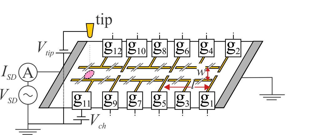
We measured two similar samples (labeled A and B) that are based on a molecular-beam-epitaxy-grown GaAs/AlGaAs heterostructure (the same as in Refs. Kozikov et al., 2014, 2013; Steinacher et al., 2015) with a two-dimensional electron gas (2DEG) 120 nm below the surface. The electron gas in sample A has a density and a mobility ; for sample B, and , both at a temperature of 300 mK. The structure was fabricated on a Hall bar of 200 m width and 2 mm contact separation with Au/Ge/Ni ohmic contacts. Schottky gates (Ti/Au) defined by electron-beam lithography complete the device structure schematically shown in Fig. 1. It consists of three consecutive channels of width m (channel 1 defined by gates g3 and g4, channel 2 by g7 and g8, and channel 3 by g11 and g12) and three quantum point contacts with a lithographic gap of 300 nm (QPC 1 defined by g1 and g2, QPC 2 by g5 and g6, and QPC 3 by g9 and g10). Neighboring quantum point contacts are separated by m along the channel axis. The Schottky gates deplete the 2DEG at voltages below V.
The samples were mounted in a home-built scanning force microscope operated in a 3He-cryostat Ihn (2004) with a base temperature of mK. A phase-locked loop controlled the microscope’s tuning fork sensor Rychen et al. (1999, 2000), to which a Pt/Ir wire was glued that had been sharpened in a focussed-ion-beam. With a voltage V applied between tip and 2DEG, we raster-scanned the tip 60 nm above the sample surface. At this voltage, the tip depleted the 2DEG within a disk of about 800 nm diameter Steinacher et al. (2015). While the tip scanned above the surface of the structure, we determined the two-terminal conductance by applying an alternating source–drain voltage Vrms to the Hall bar and measuring the alternating current with a home-built current–voltage converter and a commercial lock-in amplifier. In this way, we recorded maps of linear conductance vs. tip-position .
In the following, we investigate branched electron flow in sample A applying depleting voltages to the split gates g1 and g2, such that QPC 1 has a quantized conductance of . All the other gates have 0 V applied. The resulting scanning gate image in Fig. 2(a) has the outline of the gates superimposed with grey solid lines. In Fig. 2(b) the tip-position dependent variations of the conductance are emphasized by showing the horizontal derivative of the conductance in Fig. 2(a). On a large scale, both images consist of three regions that we label I–III in Fig. 2(a), with region II being within the channel, and regions I and III outside. Most remarkably, the spatial conductance variations induced by the scanning tip are confined to the channel region II, whereas the conductance images are smooth in the outer regions I and III. This made us suspect that placing the tip-induced potential outside the channel does not lead to scattering of electrons back through the QPC.
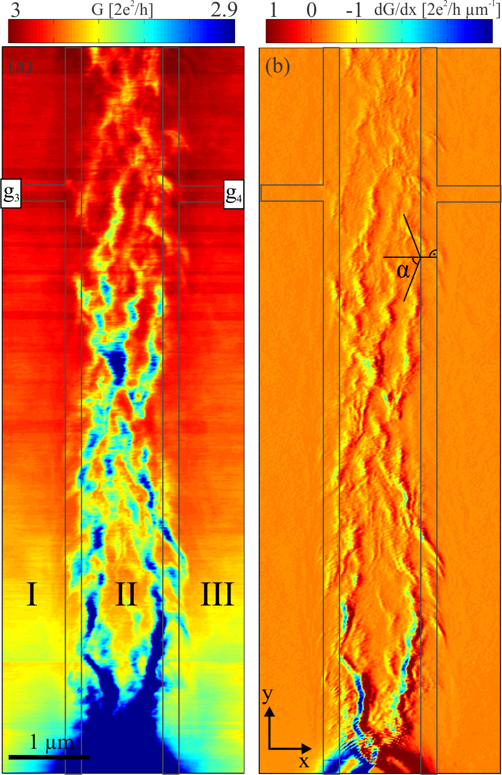
The branching pattern of conductance variations observed within the channel region II are reminiscent of the branched electron flow that Topinka Topinka et al. (2000, 2001) and later also Kozikov Kozikov et al. (2013) found in scanning gate experiments, where a QPC tuned to a quantized value of the conductance injects electrons into a 2DEG reservoir. Heller explained the formation of these branches in Ref. Heller and Shaw, 2003 as a conspiracy between random focusing of electron flow in a weak long-range spatially fluctuating potential in the absence of the tip, and time reversal symmetry at zero magnetic field which leads to backscattering through the QPC of a selected subset of electron trajectories by the tip.
The finding in Fig. 2, that the branching pattern is confined to the channel region although we apply zero volts to the channel gates g3 and g4, suggests, that these gates induce a small potential barrier with height much less than the Fermi energy. The GaAs surface pins the Fermi energy roughly in the center of the band gap Spicer et al. (1979a, b); Colleoni et al. (2014). Depositing the metallic gate on top of the surface nevertheless changes the surface potential by an amount small compared to the band gap, and thereby induces a small potential barrier in the 2DEG. In addition, strain fields originating from a difference of the thermal expansion coefficients of the gate metal and the semiconductor will induce a small potential in the 2DEG via deformation or piezoelectric coupling Winkler et al. (1989); Yagi and Iye (1993); Davies and Larkin (1994); Larkin et al. (1997); Petticrew et al. (1998); Kato et al. (1998). Therefore we interpret the confinement of the branching pattern of the conductance to be the result of a shallow potential barrier below the unbiased gate electrodes.
In regions I and III of Fig. 2(a), the smoothly varying change of the background conductance arises due to the long-range capacitive influence of the tip on the potential in QPC 1. The closer the tip moves towards the constriction, the more will the saddle-point of the QPC potential be lifted towards the Fermi energy. As a consequence the conductance gradually reduces Topinka et al. (2000, 2001); Kozikov et al. (2013).
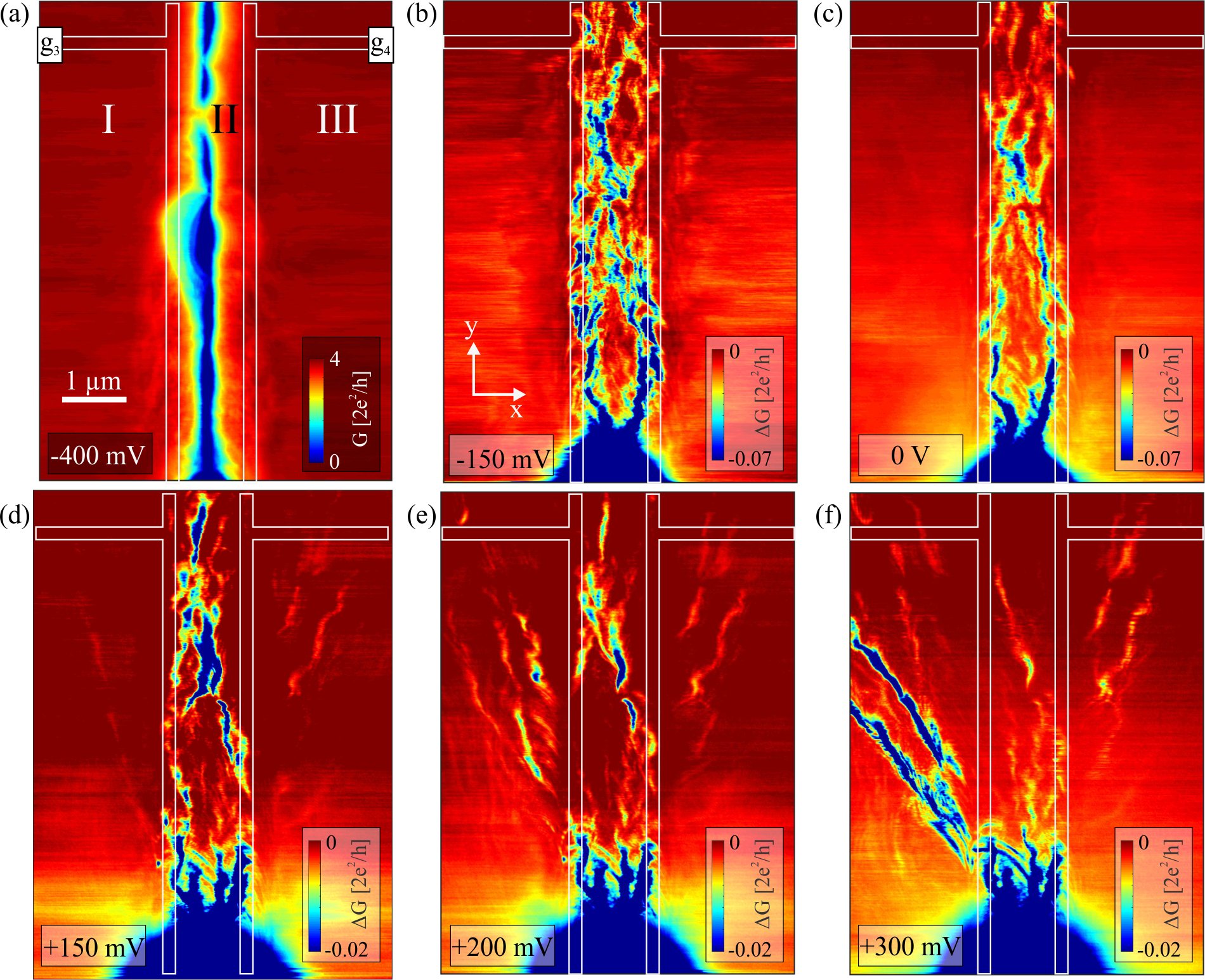
In the next step we compensate the shallow potential barrier existing at zero applied voltage for electrons below gates g3 and g4 by the application of finite positive voltages. Figure 3(b)–(f) shows scanning gate images for a selection of gate-voltages between mV and mV, where the QPC supports two spin-degenerate modes. In this transmission mode the guiding of the branches can be seen best without making the density of branches inside the channel too high (for V V). Figure 3(c) reproduces Fig. 2(a) for convenience, whereas Fig. 3(d) was obtained with mV applied to the channel gates g3 and g4. Faint branches appear in this image in regions I and III, where no structure had been seen at zero applied gate voltage. The branches penetrate into these regions even more in Figs. 3(e) and (f), where even more positive voltages were applied to the channel gates. In these images, the presence of the channel gates cannot easily be guessed from the measured image without prior knowledge.
We see contrasting behavior in Figs. 3(b) and (c), where the channel gate voltage becomes increasingly negative. In Fig. 3(b) the conductance pattern reminds us of mesoscopic conductance fluctuations, but the underlying branch pattern seen in Fig. 3(c) still leaves its traces. The potential barrier below the channel-gate is still lower than the Fermi energy in Fig. 3(b).
Figure 3(a) shows a scan where the electron gas below the gates is completely depleted. In contrast to (b)–(f) we plot conductance rather than conductance change . No matter what color-scale we choose for this image the branches have disappeared and given way to smooth variations of the conductance on a scale of m along the channel axis. Placing the tip in the center of the channel blocks transport completely, because electrons can not escape into regions I and III.
This series of measurements demonstrates that the branches of enhanced backscattering observed in scanning gate measurements near a QPC can be guided by intentionally patterned shallow potentials. This main experimental finding is natural given the notion that the observation of branches are a result of the shallow random potential landscape in the 2DEG. However, it opens new opportunities for controlling mesoscopic fluctuations in ultra-high mobility structures where artificial shallow potential landscapes steer the electron flow and thus dominate over the static potential fluctuations.
We may ask a number of questions at this point: how is it possible that the branching pattern is confined by a shallow potential barrier? Does the large and invasive tip-induced potential still image the electron flow in the absence of the tip as it does in an open 2DEG? How does the presence of the tip change the electron flow? What can we learn from our measurements for the general case of scanning gate measurements in confined geometries? Let us answer these questions by presenting additional analysis and by digging deeper into the microscopic physics of the experiment.
The branch-guiding property of a shallow potential may be seen as an effect of geometric electron optics. The potential barrier below the channel gates plays the role of a medium reflecting or transmitting incoming electron beams according to Snell’s law. Electrons at the Fermi energy impinging on the barrier of height at an angle (measured with respect to the barrier normal) larger than the critical angle are totally reflected back into the channel with their momentum parallel to the channel axis conserved [see schematics in Fig. 2(b)]. In our structure we estimate at zero channel gate voltage 111For this estimate we assume complete compensation of the barrier (flat band) at +200 mV and pinch-off at -350 mV. At 0 V we therefore find . The precision of compensation-voltage is on the order of mV giving . Collimation of the electron beam due to QPC 1 is expected to lead to an injection characteristic essentially cut off by a critical injection angle (measured with respect to the channel axis) Beenakker and van Houten (1991); Crook et al. (2000). We may obtain an experimental estimate of the angular distribution of injected electrons from Fig. 3(c). In this figure we see that the observed backscattering branches outside the wire fan out at a maximum angle . This maximum injection angle leads to a fraction of 85% of electrons that would remain within the channel boundaries after the first reflection. The remaining 15% are typically not visible because of the experimental limit in sensitivity.
Classical trajectory-based simulations of the conductance Beenakker and van Houten (1989); Baranger et al. (1991) help us to understand electron branching and the classical background resistance. We find that they qualitatively reproduce the experimental behavior [see Fig. 5(d)] and give further insight into the flow of electrons in the structure with and without the tip, and therefore on the imaging mechanism at work. We calculate trajectories by solving Newton’s equations in two dimensions for a given potential landscape. Gate-induced potentials are modeled using the analytic expressions of Davies Davies et al. (1995). A Lorentzian profile represents the tip-induced potential Topinka et al. (2001); Eriksson et al. (1996b)222Note that the tip-depletion size for the simulation is smaller than the one in the experiment to get similar scanning gate maps. Electrostatic screening of the tip-induced potential, finite resolution and signal-to-noise in the experiment naturally lead to less sensitivity compared to the simulation. We introduce a random disorder potential landscape caused by ionized impurities in the doping plane which accounts for Thomas-Fermi screening Ando et al. (1982), finite thickness of the 2DEG Fang and Howard (1966); Ando et al. (1982), and charge correlations in the doping plane Efros et al. (1990). All the parameters of the disorder potential are given by the sample geometry and the electron density at zero gate-voltage, except for the correlation parameter which is used to tune the theoretical electron mobility to be the same as in the experiment. The conductance is a weighted sum of individual trajectory contributions.
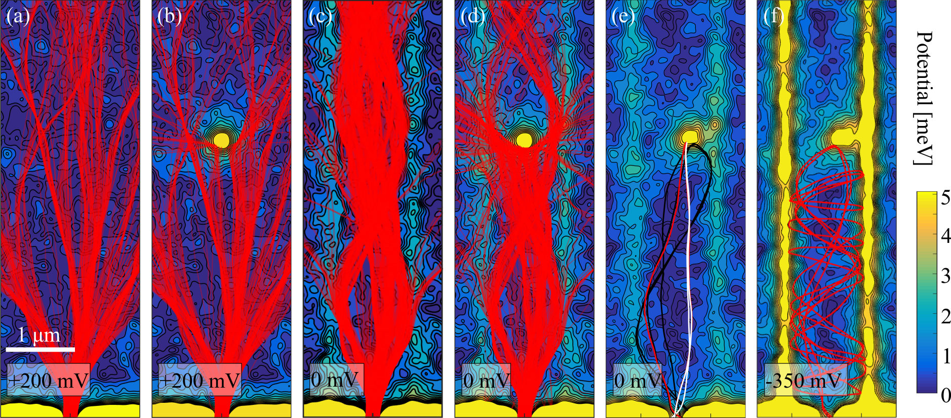
In agreement with Topinka Topinka et al. (2001), Heller Heller and Shaw (2003), and Metzger Metzger et al. (2010); Metzger (2010) our model reproduces the formation of caustics and branched electron flow in the absence of the scanning tip in an open 2DEG past a QPC [Fig. 4(a)]. Caustics are bundles of higher than average (in theory even diverging) trajectory-density caused by accidental lensing in the random disorder potential. Heller argued in Ref. Heller and Shaw, 2003 that a hard-wall cylinder-shaped tip-potential would reflect branches with close to normal incidence back through the QPC on time-reversed paths. He explained in this way the superb spatial resolution of scanning gate microscopy which is much better than the diameter of the tip. A more realistic soft tip-potential modifies this description in two ways: First, the disorder potential distorts the Fermi-contour of the tip-induced potential changing the direction of normal incidence [see the distorted Fermi-contour in Fig. 4(b), (d), and (e)]. Second, the long-range tail of the tip-potential slightly diverts the branches present in the absence of the tip. Both effects lead to differences between the branched flow in the absence of the tip and the scanning-gate images. Less severe for the appearance of the scanning-gate image is the fact that the electron flow is strongly modified by the presence of the tip [c.f. Figs. 4(a) and (b)]: trajectories that are only diverted but not backscattered will not reduce the measured conductance.
The trajectory model confirms that the branches are guided by shallow channel-potentials [see Fig. 4(c)]. Like in the open 2DEG the tip scatters most trajectories out of the channel but not back trough the QPC [Fig. 4(d)] and hence does not change the conductance. Nevertheless, an increasingly negative channel-gate voltage increases the proportion of trajectories scattered back through the QPC. In the open system only direct backscattering from the tip is possible [like the white trajectory in Fig. 4(e)], whereas the channel-potential gives rise to trajectories scattering once [see red curve in Fig. 4(e)] or multiple times [black curve in Fig. 4(e)] from the channel-gates before they are backscattered through the QPC. These trajectories include paths with normal incidence on the tip but also others that enclose a finite area. This implies that the ability to image branch-like classical trajectory-families is reduced the stronger the channel is confined. When the channel-gate voltage depletes the underlying electron gas most trajectories spend a long time in the cavity between the QPC and the tip, bouncing chaotically from wall to wall leaving the structure only accidentally through the QPC [see Fig. 4(f)] or the opening between the tip and the channel gate.
Since the spatial potential fluctuations are caused by the random distribution of ionized donors, the branching pattern differs from sample to sample, and even for different cool downs. To compare experiment and simulation not only qualitatively [see Fig. 5(d) for simulated scanning gate images] we therefore average the measured conductance, such that only the classical background remains. Accordingly, we compare these averaged quantities with simulations without a disorder potential.
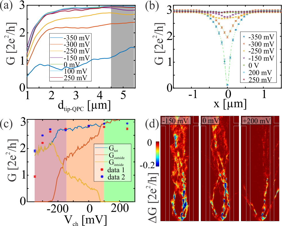
To this end we analyzed a series of scanning gate images at QPC 3 with different voltages applied to channel 3 of sample B. In Fig. 5(a) we plot the conductance of the system along a line parallel to the channel axis. We smoothen the cuts with a running average of nm width to remove most of the modulations that are caused by branches from the background. It is not possible to remove them completely: variations on length scales larger than nm remain.
In Fig. 5(a) the conductance increases with increasing tip–QPC distance reaching a constant value at m. The strong increase of the conductance within the first two microns is due to strong backscattering with the tip in close vicinity to the constriction as well as due to the gating effect. We obtain the curves shown in Fig. 5(b) by taking average saturation values [see grey-shaded region in (a)] of similar curves taken parallel to the channel-axis at different -coordinates. The channel is seen as a pronounced dip in the conductance with a strength that increases with increasing confinement of the channel, as expected. Figure 5(c) shows the conductance values at of two channels (data 1 and data 2) on sample B plotted against the channel-voltage. The trajectory physics differs significantly in the regions colored differently. In the green-shaded region most electrons scattered off the tip are not backscattered through the QPC. Backscattering occurs preferentially along branches modulating the conductance at a level of a few percent. In the red region the electron flow is strongly channeled by the gate-induced potential in the absence of the tip. This effect leads to the observed guiding of branches. However, the channel-potential is still too low to prevent the majority of electrons scattering off the tip from propagating into regions I and III. This changes in the violet region where the electrons are increasingly kept inside the channel, enhancing their chance to scatter back through the QPC.
We compare the experimental behavior in Fig. 5(c) with the transmission and reflection probabilities calculated with the classical trajectory model. The transmission probability is split into two contributions, namely, the probability of being transmitted and leaving the structure through regions I or III (red denotes G), and the probability of transmitting beyond the tip within the wire region II (yellow denotes G). The model supports our interpretation by showing that in the green region almost all electrons are scattered out of region II whereas in the red region the electrons increasingly stay in the channel with growing wire potential. In the violet region, however, the number of electrons that make it past the tip starts to decrease, because the channels between tip and wire potential shrink.
In summary, we have studied branched electron flow in a wire geometry tunable between weak and strong confinement using scanning gate microscopy. A comprehensive understanding of the measured conductance was reached based on classical trajectories. Weak confinement guides the branches known from open two-dimensional electron gases. In contrast, stronger confinement generates a chaotic cavity with strongly enhanced backscattering. Hand in hand with the change in trajectory dynamics the scanning gate technique gradually loses its spatial resolution for backscattered electron flow from the weakly to the strongly confined regime. These insights bear importance for previous experiments Crook et al. (2000); Burke et al. (2010); Ferry et al. (2011); Aoki et al. (2012) on scanning gate imaging of open quantum dots. Our results will lead to educated designs of future scanning gate experiments on cavities. Guiding branches with shallow potentials promises experiments in the realm of mesoscopic physics, in which caustics are controlled by external voltages. Our results raise the interesting theoretical question, which information about the disorder potential can be extracted from measurements of the branch pattern.
Acknowledgements.
We thank Beat Bräm, Dietmar Weinmann, Rodolfo Jalabert, Guillaume Weick, and Boris Brun for helpful discussions. We acknowledge financial support from the Swiss National Science Foundation, the NCCR ”Quantum science and Technology” and ETH Zürich.References
- Lynch and Livingston (2001) D. Lynch and W. Livingston, Color and Light in Nature (Cambridge University Press, 2001).
- Berry (1975) M. Berry, J. Phys. A: Math. Gen. 8, 566 (1975).
- Topinka et al. (2001) M. Topinka, B. LeRoy, R. Westervelt, S. Shaw, R. Fleischmann, E. Heller, K. Maranowski, and A. Gossard, Nature 410, 183 (2001).
- Heller and Shaw (2003) E. J. Heller and S. Shaw, Int. J. Mod. Phys. B 17, 3977 (2003).
- Eriksson et al. (1996a) M. Eriksson, R. Beck, M. Topinka, J. Katine, R. Westervelt, K. Campman, and A. Gossard, Appl. Phys. Lett. 69, 671 (1996a).
- Crook et al. (2003) R. Crook, C. Smith, A. Graham, I. Farrer, H. Beere, and D. Ritchie, Phys. Rev. Lett. 91, 246803 (2003).
- Burke et al. (2010) A. Burke, R. Akis, T. Day, G. Speyer, D. Ferry, and B. Bennett, Phys. Rev. Lett. 104, 176801 (2010).
- Ferry et al. (2011) D. Ferry, A. Burke, R. Akis, R. Brunner, T. Day, R. Meisels, F. Kuchar, J. Bird, and B. Bennett, Semicond. Sci. Technol. 26, 043001 (2011).
- Aoki et al. (2012) N. Aoki, R. Brunner, A. Burke, R. Akis, R. Meisels, D. Ferry, and Y. Ochiai, Phys. Rev. Lett. 108, 136804 (2012).
- Kozikov et al. (2014) A. Kozikov, R. Steinacher, C. Rössler, T. Ihn, K. Ensslin, C. Reichl, and W. Wegscheider, New J. Phys. 16, 053031 (2014).
- Kozikov et al. (2013) A. Kozikov, C. Rössler, T. Ihn, K. Ensslin, C. Reichl, and W. Wegscheider, New J. Phys. 15, 013056 (2013).
- Steinacher et al. (2015) R. Steinacher, A. Kozikov, C. Rössler, C. Reichl, W. Wegscheider, T. Ihn, and K. Ensslin, New J. Phys. 17, 043043 (2015).
- Ihn (2004) T. Ihn, Electronic quantum transport in mesoscopic semiconductor structures, Vol. 192 (Springer Verlag, 2004).
- Rychen et al. (1999) J. Rychen, T. Ihn, P. Studerus, A. Herrmann, and K. Ensslin, Rev. Sci. Instrum. 70, 2765 (1999).
- Rychen et al. (2000) J. Rychen, T. Ihn, P. Studerus, A. Herrmann, K. Ensslin, H. Hug, P. van Schendel, and H. Guntherodt, Rev. Sci. Instrum. 71, 1695 (2000).
- Topinka et al. (2000) M. Topinka, B. LeRoy, S. Shaw, E. Heller, R. Westervelt, K. Maranowski, and A. Gossard, Science 289, 2323 (2000).
- Spicer et al. (1979a) W. Spicer, P. Chye, P. Skeath, C. Y. Su, and I. Lindau, J. Vac. Sci. & Technol. 16, 1422 (1979a).
- Spicer et al. (1979b) W. Spicer, P. Chye, C. Garner, I. Lindau, and P. Pianetta, Surf. Sci. 86, 763 (1979b).
- Colleoni et al. (2014) D. Colleoni, G. Miceli, and A. Pasquarello, J. Phys.: Cond. Mat. 26, 492202 (2014).
- Winkler et al. (1989) R. Winkler, J. Kotthaus, and K. Ploog, Phys. Rev. Lett. 62, 1177 (1989).
- Yagi and Iye (1993) R. Yagi and Y. Iye, J. Phys. Soc. Jap. 62, 1279 (1993).
- Davies and Larkin (1994) J. H. Davies and I. A. Larkin, Phys. Rev. B 49, 4800 (1994).
- Larkin et al. (1997) I. A. Larkin, J. H. Davies, A. R. Long, and R. Cuscó, Phys. Rev. B 56, 15242 (1997).
- Petticrew et al. (1998) D. Petticrew, J. Davies, A. Long, and I. Larkin, Physica B: Cond. Mat. 249, 900 (1998).
- Kato et al. (1998) M. Kato, A. Endo, S. Katsumoto, and Y. Iye, Phys. Rev. B 58, 4876 (1998).
- Note (1) For this estimate we assume complete compensation of the barrier (flat band) at +200 mV and pinch-off at -350 mV. At 0 V we therefore find . The precision of compensation-voltage is on the order of mV.
- Beenakker and van Houten (1991) C. Beenakker and H. van Houten, Solid State Physics 44, 1 (1991).
- Crook et al. (2000) R. Crook, C. Smith, C. Barnes, M. Simmons, and D. Ritchie, J. Phys.: Cond. Mat. 12, L167 (2000).
- Beenakker and van Houten (1989) C. Beenakker and H. van Houten, Phys. Rev. Lett. 63, 1857 (1989).
- Baranger et al. (1991) H. Baranger, D. DiVincenzo, R. Jalabert, and A. Stone, Phys. Rev. B 44, 10637 (1991).
- Davies et al. (1995) J. H. Davies, I. A. Larkin, and E. Sukhorukov, J. Appl. Phys. 77, 4504 (1995).
- Eriksson et al. (1996b) M. Eriksson, R. Beck, M. Topinka, J. Katine, R. Westervelt, K. Campman, and A. Gossard, Superlatt. Microstruct. 20, 435 (1996b).
- Note (2) Note that the tip-depletion size for the simulation is smaller than the one in the experiment to get similar scanning gate maps. Electrostatic screening of the tip-induced potential, finite resolution and signal-to-noise in the experiment naturally lead to less sensitivity compared to the simulation.
- Ando et al. (1982) T. Ando, A. B. Fowler, and F. Stern, Rev. Mod. Phys. 54, 437 (1982).
- Fang and Howard (1966) F. Fang and W. Howard, Phys. Rev. Lett. 16, 797 (1966).
- Efros et al. (1990) A. Efros, F. Pikus, and G. Samsonidze, Phys. Rev. B 41, 8295 (1990).
- Metzger et al. (2010) J. J. Metzger, R. Fleischmann, and T. Geisel, Phys. Rev. Lett. 105, 020601 (2010).
- Metzger (2010) J. J. Metzger, Branched Flow and Caustics in Two-Dimensional Random Potentials and Magnetic Fields, Ph.D. thesis, Max-Planck Institut f. Dynamik und Selbstorganisation (2010).