Tunable plasmonic reflection by bound 1D electron states in a 2D Dirac metal
Abstract
We show that surface plasmons of a two-dimensional Dirac metal such as graphene can be reflected by line-like perturbations hosting one-dimensional electron states. The reflection originates from a strong enhancement of the local optical conductivity caused by optical transitions involving these bound states. We propose that the bound states can be systematically created, controlled, and liquidated by an ultranarrow electrostatic gate. Using infrared nanoimaging, we obtain experimental evidence for the locally enhanced conductivity of graphene induced by a carbon nanotube gate, which supports this theoretical concept.
Plasmon scattering and plasmon losses in Dirac materials, such as graphene and topological insulators, are problems of interest to both fundamental and applied research. It is an outstanding challenge to understand various kinds of interaction (electron-electron, electron-phonon, electron-photon, electron-disorder) responsible for these complex phenomena Das Sarma et al. (2011); Kotov et al. (2012); Basov et al. (2014); Principi et al. (2014); Woessner et al. (2014). At the same time, control of plasmon scattering is critical if this class of materials is to become a new platform for nanophotonics Jablan et al. (2009); Vakil and Engheta (2011); Grigorenko et al. (2012); García de Abajo (2014).
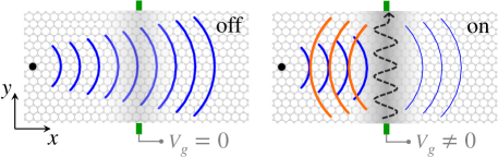
One source of plasmon scattering is long-range inhomogeneity of the electron density, which causes local fluctuations in the plasmon wavelength . If the inhomogeneities are weak, those of size comparable to the average are expected to be the dominant scatterers Kechedzhi and Das Sarma (2013); Garcia-Pomar et al. (2013) Surprisingly, recent experiments have revealed that one-dimensional (1D) defects of nominally atomic width can act as effective reflectors for plasmons with wavelengths as large as a few hundred nm. Strong plasmon reflection was observed near grain boundaries Fei et al. (2013); Schnell et al. (2014), topological stacking faults Ju et al. (2015), as well as nanometer-scale wrinkles and cracks Fei et al. (2013); Garcia-Pomar et al. (2013) in graphene. If this anomalous reflection is indeed an ubiquitous effect largely unrelated to the specific nature of a defect, it calls for a universal explanation. In this Letter we attribute its origin to electron bound states commonly occurring near 1D defects. We show that optical transitions involving the bound states can produce strong dissipation at small distances from the defect and therefore, alter plasmon dynamics. To support this idea we present a theoretical analysis of an exactly solvable model, which illustrates qualitative and quantitative characteristics of the bound states and predicts how their optical response depends on the tunable parameters of a 1D potential well. We also report an attempt to probe the predicted effects experimentally. Our approach is to employ an ultranarrow electric gate in the form of a carbon nanotube (CNT) to create a precisely tunable 1D barrier in graphene. This device enables a systematic investigation and control of plasmon propagation, including, in principle, an implementation of a plasmon on-off switch (Fig. 1). What we find is that the measured real-space profile of the plasmon amplitude (Fig. 4) cannot be accounted for by a local change in alone. Instead, the data are consistent with the presence of an enhanced dissipation in the region next to the CNT. The amount of this dissipation agrees in the order of magnitude with the power absorption due to 1D bound states in our model.
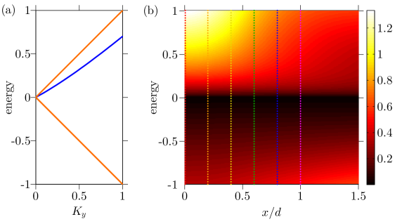
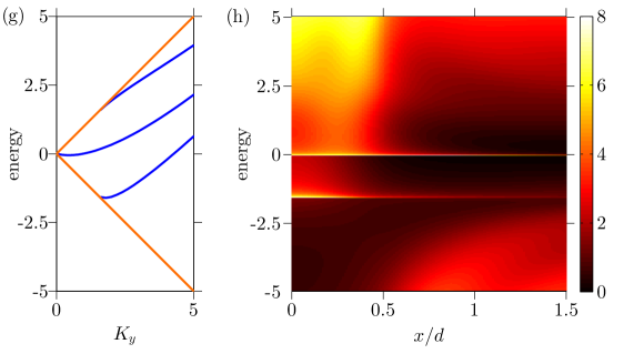
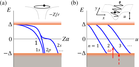
Model.—We assume that the graphene quasiparticles can be described by a 2D Dirac Hamiltonian , where , are the Pauli matrices and is the total (screened) potential induced by the 1D gate. For simplicity, we assume that is a square well of width and depth although more realistic potentials Kennedy (2002); Hartmann and Portnoi (2014); Candemir and Bayrak (2013); Villalba and Greiner (2003) can also be considered. In the present case the eigenfunctions are combinations of plane waves and/or exponentials that have to be matched at , see Appendix A. The electron momentum along the perturbation (in the -direction) is conserved, so that the gapless 2D Dirac spectrum is effectively replaced by a 1D one with a gap . Within the gap electron states localized at the well exist [Fig. 2(b)]. The energies of these bound states, where , are the solutions of the transcendental equation Beenakker et al. (2009)
| (1) |
Here is the dimensionless energy and
| (2) |
are, respectively, the dimensionless -momentum and the well depth. The dispersions of the three lowest bound states for are shown in Fig. 2(a).
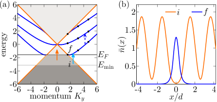
The response of the system to an optical excitation of frequency polarized in the -direction is described by an effective conductivity given by the Kubo formula sup , which determines the local current density in the approximation that the total electric field due to the optical excitation is uniform. Below we focus on the real part of , which determines local power dissipation. We assume that graphene is doped and consider only frequencies , for which the optical conductivity of an infinite graphene sheet vanishes (if we neglect disorder, many-body scattering, and thermal broadening Basov et al. (2014)). This implies that in the absence of the perturbation, , we must have at all . On the other hand, when the potential well is present, a finite exists. There are two types of relevant optical transitions: those that involve the bound states [as either the initial or the final states, Fig. 2(a)] and those that do not. The contribution of the former to is maximized near the potential well and decays exponentially at due to the localized nature of the bound states. The contribution of the latter is small, oscillating, and decaying algebraically with sup . Resolving the detailed real-space features of in an optical experiment is challenging (see below). A more practical observable is the normalized integrated conductivity:
| (3) |
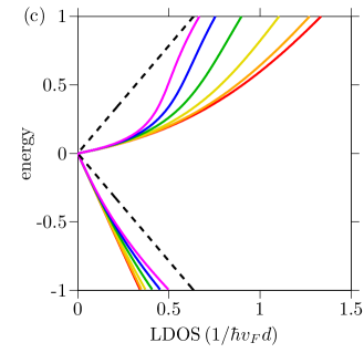
According to our simulations, transitions that involve the bound states give the dominant contribution to . In particular, bound-to-bound state transitions produce numerically large values of expressed in units of . Such transitions are possible at discrete where the energy difference between the states of the same momentum matches provided the lower (higher) state is occupied (empty). If the chemical potential is gradually increased, e.g., by electrostatic gating, the state occupations would change, leading to either blocking or unblocking of these transitions. Accordingly, would either sharply drop or jump, see Fig. 3(a). These changes persist, albeit blurred, at finite temperatures, see the dashed curve in Fig. 3(a).
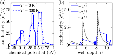
Sharp drops in also occur when the bound states merge with the continuum and get liquidated (become extended). The drop is abrupt if the optical transitions probe a single or a narrow range of . In principle, this situation can be realized in a graphene ribbon running perpendicular to the linelike perturbation. In such a ribbon the allowed are discrete, as shown schematically by the dots in Fig. 2(b). The coupling to a single bound state can be achieved under the condition , i.e., by using a ribbon of a narrow width or the excitation of a low frequency . In Fig. 3(b) we show three numerically calculated traces of as a function of the well depth for a fixed dimensionless chemical potential . The first trace is computed for a ribbon of width probed at the excitation energy . It exhibits pronounced oscillations of . In particular, drops to zero when a bound state merges with the continuum. The other two traces correspond to a 2D graphene sheet. Although the sharp drops become blurred, they remain pronounced at a low excitation energy and still evident at .
The enhanced local optical conductivity around the 1D gates described above causes plasmons to be strongly reflected. According to the first-order perturbation theory Fei et al. (2013); Garcia-Pomar et al. (2013); sup , the reflection coefficient of a normally incident plasmon wave is
| (4) |
For arbitrary perturbations, we can use the approximation . Using the results of Fig. 3(b) we estimate at the chemical potential of where the predicted . This roughly corresponds to the regime probed by our experiments (see below). At the chemical potential of where the calculated local conductivity is much larger, , the reflection coefficient should approach unity, realizing the “reflector on” state in Fig. 1.
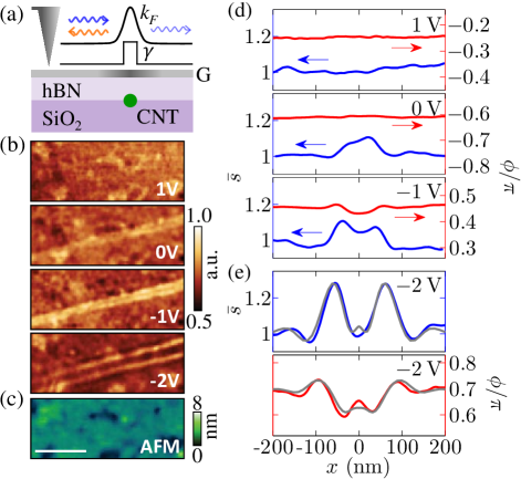
Experiment and analysis.—To investigate the described above phenomena experimentally we fabricated a nanodevice that contained (bottom to top) a Si/SiO2 substrate, a -thick layer of hexagonal boron nitride (hBN), and a mechanically exfoliated graphene flake. A metallic single-wall CNT was placed between hBN and SiO2. The local charge density of graphene was tunable by the voltage applied between the CNT and graphene. The average carrier density in graphene was produced by uncontrolled ambient dopants (acceptors) Ni et al. (2015). To infer the local optical conductivity we used scattering-type scanning near-field optical microscopy (s-SNOM) Keilmann and Hillenbrand (2009); Atkin et al. (2012); Basov et al. (2014), see Fig. 4(a). The s-SNOM utilizes a tip of an atomic force microscope (AFM) with a radus as an optical antenna that couples incident infrared light to graphene plasmons. The backscattered light is analyzed to extract the amplitude and the phase of the genuine near-field signal, Fig. 4(b,d,e). Crudely speaking, this signal is proportional to the electric field inside the tip-sample nanogap. The variation of this field with the tip position is caused by the standing-wave patterns of surface plasmons Fei et al. (2012); Chen et al. (2012). These standing waves are due to the interference of the plasmon waves launched by the tip with the waves reflected by the charge inhomogeneity induced by the CNT. The spacing of the interference fringes is equal to one half of the plasmon wavelength . The latter is given by , where is the complex plasmon momentum and is the average permittivity of the media surrounding graphene Basov et al. (2014). Therefore, s-SNOM images combined with the formula for give a direct estimate of . The extraction of requires an electromagnetic simulation of the coupled tip-graphene system, which was done using the numerical algorithm developed previously Fei et al. (2012, 2013); sup . To facilitate connection with that previous work, we parametrized the conductivity via
| (5) |
which was modelled after the long-wavelength Drude (intraband) conductivity of graphene Basov et al. (2014) with Fermi momentum and dimensionless damping factor . The goal of the data analysis was to determine the profiles of and that yield the best fit to the s-SNOM data. In this parametrization, the presence of the bound states should increase the local damping, so the signature we were looking for was the enhanced value of .
Our experimental data are presented in Fig. 4. The AFM topography image, Fig. 4(c), shows that the CNT does not produce any visible topographic features. However, in the near-field signal, up to two pairs of intereference fringes appear on each side of the CNT [the bright lines in Fig. 4(b)]. Similar twin fringes have been observed in prior s-SNOM imaging Fei et al. (2013); Schnell et al. (2014); Ju et al. (2015); Ni et al. (2015) of linear defects in graphene. Importantly, the intensity and spacing of the fringes we observe here evolve with the CNT voltage , which attests to their electronic (specifically, plasmonic) origin.
In addition to the controlled perturbation induced by the CNT, graphene contains uncontrolled ones due to random defects. To reduce the random noise caused by those, we averaged the near-field signal over a large number of linear traces taken perpendicular to the CNT. Thus obtained line profiles of both the amplitude and the phase are plotted in Fig. 4(d) and (e). We focus on the trace, which shows the strongest modulation. The accurate determination of functions and is impacted by the s-SNOM resolution limit . In our fitting we assumed that is given by the perfect screening model, , which should be a good approximation for high doping Jiang and Fogler (2015). The adjustable parameters are and . For we considered trial functions in the form of a peak (dip) at , with adjustable width and height (depth), as sketched in Fig. 4(a). The trial and were fed as an input to the electromagnetic solver described previously Fei et al. (2012, 2013). As detailed in Appendix D, a good agreement with the observed form of the twin fringes requires a strong peak in near the CNT. The shape of the fringes was found to depend primarily on the integral of , so in the end we modeled by a box-like discontinuity with a central region of a fixed width and two adjustable parameters , . The best fits [the gray curves in Fig. 4(e)] to the s-SNOM data were obtained using .
To establish a rough correspondence between the profiles of Fig. 4(e) and the square-well model we take to be the thickness of the hBN spacer and to give the same integrated weight . This prescription implies , , and for sup . The square-well model in Fig. 3 yields a comparable optical conductivity although for a smaller . Given a number of simplifying assumptions we have made in the modelling, this level of agreement seems adequate.
Summary and future directions.—In this Letter, we proposed a model for the anomalous plasmon reflection by ultranarrow electron boundaries in graphene. We validated this concept in experiments with electrostatically tunable line-like perturbations. One broad implication of our work is that nanoimaging of collective modes can reveal nontrivial electron properties, in this case, 1D bound states. Recent experiments have demonstrated that this technique is not limited to plasmons or graphene or 2D systems Dai et al. (2014); Shi et al. (2015); Giles et al. (2016); Fei et al. . We hope that our work stimulates even wider use of this novel spectroscopic tool.
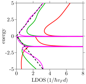
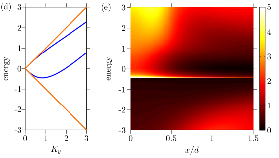
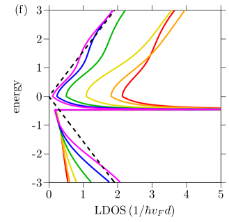
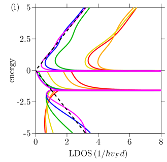
A particularly intriguing future direction is to complement s-SNOM with scanned probe techniques other than AFM topography. For example, scanning tunneling microscopy, which has a superior spatial resolution, can be used to measure the local electron density of states (LDOS). For the particular model system studied here, the features exhibited by the LDOS should be quite striking, see Fig. 5 and Appendix B. The origin of these features can be understood by examining the dispersions in Fig. 2(a). Within the selected energy interval there is the total of three bound states. The topmost one has a monotonic dispersion; the other two have energy minima at which the LDOS has van Hove singularities (diverges), see Fig. 5. The strength of these singularities decreases exponentially with because these bound states are localized near the well. At large , the LDOS displays the -shaped energy dependence characteristic of uniform graphene Basov et al. (2014). We anticipate that the combination of optical and tunneling nanoimaging and nanospectroscopy could provide a refined information about the local electronic structure. One example of a possible application of this knowledge is the design of optimized plasmon switches (Fig. 1) for Dirac-material-based nanoplasmonics.
We acknowledge support by the ONR under Grant N00014-13-0464 and by the NSF under Grant ECCS-1509958 (M.B.).
Appendix A Local optical conductivity of a nonuniform graphene
In this section we describe the details of our 1D square well model, including the analytical expressions for the wavefunctions and the calculation of the optical conductivity in the vicinity the well. We start from the 2D Dirac Hamiltonian for the quasiparticles,
| (6) |
where are the Pauli matrices acting on the sublattice pseudospin. The potential is taken to be a square well,
| (7) |
Without loss of generality, we take to be positive. As the system is invariant in the -direction, is conserved, and so our problem is effectively one-dimensional. We use the following terminology: region I is the part of the system to the left of the well (); region II is the strip containing the well (); region III is to the right of the well (). For an eigenstate to have the same energy across all three regions, the magnitude of its momentum must obey the following relations
| (8) |
with , II, or III. When , the wavefunction belongs in the conduction band and has the form
| (9) |
when , the wavefunction belongs to the valence band and is given by
| (10) |
The angle defines the direction of the momentum. In the following we use the notation for and for and similarly for all other quantities.
We find the complete expression for the wavefunction using the following device. We imagine that this wavefunction is generated by a plane wave incident from region I, which is then partially transmitted and reflected at each edge of the well. This yields
| (11) |
where is normalization factor equal to the area of the system and and can be either or . The coefficients , , and are determined by requiring the wavefunction to be continuous at the edges of the well, . If the wavefunction remains in the same band for all three regions, the coefficients are
| (12) | |||
| (13) | |||
| (14) | |||
| (15) |
where and , and
| (16) |
If the wavefunction switches band upon entering the well, the coefficients are
| (17) | |||
| (18) | |||
| (19) | |||
| (20) |
If is real, there is another wavefunction with the same magnitude of the momentum (same energy), which corresponds to the wave incident from region III. A quick method to obtain is by reflecting with respect to the -axis:
| (21) |
From and we construct the orthogonal eigenstates
| (22) |
which are labeled by their parity :
| (23) |
From the above expression we deduce that states localized within the potential well must also exist. Indeed, whenever there exist states with , so that is imaginary and the wavefunction is evanescent outside the well. This happens when the denominators vanish, , so that the eigenstate exists without an incident plane wave from outside the well. The dispersion of these bound states is found by solving
| (24) |
The wavefunction still has the form of Eq. (11), but with a normalization factor
| (25) |
Note that is now imaginary, with . Each branch of solution except the one terminating at is the continuation of Fabry–Pérot (FP) modes outside the continuum. The FP modes correspond directly to the supercritical or quasi-bound states. They satisfy the resonance condition with , so branches of smaller emerge at higher . This condition can be expanded to find the expression for the critical point at which the th bound state emerges from the valence band,
| (26) |
All the bound state branches asymptotically approach the line as . The wavefunction of each branch is alternatively even () or odd () with the lowest branch being even. An example of the normalized density of a bound state is shown in Fig. 6(a) along with the normalized density of continuum states for comparison.
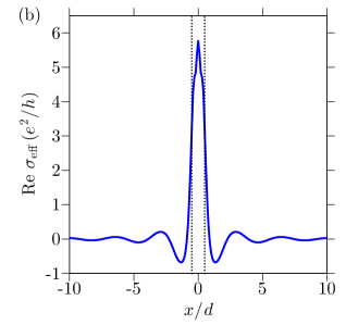
Having found the expression for the eigenstate wavefunctions, we use the Kubo formula to calculate the nonlocal conductivity,
| (27) |
where and represent initial and final states, is the Fermi-Dirac occupation factor of the state with and , is the energy of the state, and is the current operator. Assuming that the total field E is uniform and parallel to , the current-field relation can be simplified to
| (28) |
Note that the integral over enforces the conservation of ,
| (29) |
so that all and dependences cancel out in Eq. (28). We are interested in the real part of the effective conductivity. Transitions that contribute satisfy the relations
| (30) |
Additionally, the states must have the opposite parity as the matrix element
| (31) |
is odd in when the states have the same parity. To proceed, we impose periodic boundary conditions and extend the system size to infinity, so that
| (32) |
where is taken to be positive and is the total degeneracy, including spin, valley and contribution from negative . Applying the Sokhotski–Plemelj formula
| (33) |
to Eqs. (27) and (28), we find for the bound-to-bound state transitions,
| (34) |
where satisfies Eq. (30). For bound-to-continuum transitions, we get
| (35) |
The limits of are determined from the dispersion, the frequency and the doping level . Continuum-to-bound state transitions result in the same expression except that the labels and are interchanged. The resultant conductivity has a peak around the well and decays quickly away from the well [Fig. 6(b)]. Finally, continuum-to-continuum transitions yield
| (36) |
where
| (37) |
This results in an oscillating conductivity with a period of which can be negative, that is, the local current in real space can go in the opposite direction as the field. This is however no cause for alarm. Consider the case of uniform undoped graphene where the conductivity as a function of momentum at fixed is
| (38) |
The corresponding conductivity in the real-space is
| (39) |
so that can be negative. Thus conductivity oscillations with period is a general property in the presence of nonuniformity. For in our s-SNOM experiment this period is and such oscillations cannot be easily resolved. Therefore, we draw the reader’s attention to another feature of the computed local conductivity, which is the prominent peak near the origin, see Fig. 6(b). We conclude that our simple model does predict a strong enhancement of dissipation near the nanotube, in agreement with the experiment. The extra dissipation is caused by the bound-to-bound state optical transitions. Of course, these calculations are not meant to be quantitatively compared with the experiment because our model of the square-well potential is not fully realistic. The quantity more suitable for the purposes of a qualitative comparison is the average value of the effective conductivity
| (40) |
similar to Eq. (4) of the main text. As long as is larger than but smaller than the spatial resolution, the near-field profile is sensitive only to the product not the precise value of , see Appendix D. The results of our calculations of are shown in Fig. 3 of the main text. For simplicity, in these calculations we excluded the part of resulting from continuum-to-continuum transitions because it is relatively small at the potential well.
Appendix B Local density and density of states
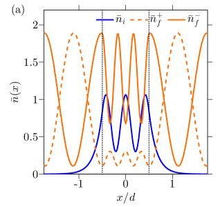
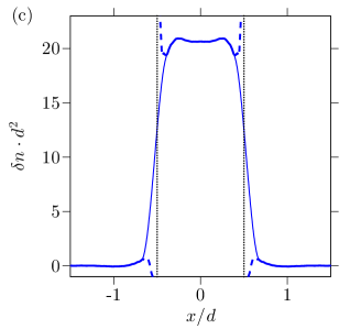
For better understanding of the effect of the potential well on electronic properties it is instructive to consider two other local observables: the carrier density and the local density of states. We begin with the density perturbation . To find this quantity we first find the square of the absolute value of the wavefunctions of the occupied eigenstates under the potential well, integrated over and . The integration is done over the energies bounded from above by the Fermi energy and from below by a cutoff energy , a large negative number. The same procedure is then repeated for the unperturbed eigenstates (without the potential well). The difference of the two results is . There is however a complication to this procedure rooted in the “chiral anomaly” in the quantum field-theory of free Dirac fermions. For inside the well, the lower cutoff for the unperturbed eigenstates must be changed to . Without this redefinition, would diverge as is decreased. Once this proper background subtraction is done, the integration converges to a finite value everywhere except at the edges of the well, . The remaining divergence can be traced to the discontinuity in the potential . To arrive at this conclusion we reasoned that the divergence is produced by large negative energies, and so it could be investigated using the perturbation theory. Therefore, we considered the linear-response theory expression for the density perturbation:
| (41) |
where
| (42) |
is the Fourier transform of the potential and is the static polarization function of graphene. At large this function behaves as
| (43) |
regardless of the doping level. Wunsch et al. (2006) Evaluation of the integral for using this asymptotic form yields
| (44) |
which matches the numerical results calculated as described above for undoped graphene [Fig. 6(c)]. In reality, i) the linear dispersion of Dirac fermions does not extend to infinite momenta and ii) the potential must be smooth. Either way the divergence is regularized and the perturbed density is smooth as well, see Fig. 6(c). Not surprisingly, this box-like density profile is different from the more realistic Lorentzian function [Eq. (66)] we used to fit the experimental data in the main text and in Appendix D below. However, as we argued in Appendix A, a qualitative comparison between the present model and the experiment is still meaningful.
Let us now turn to the local density of states (LDOS) . Previously, the LDOS of graphene around clusters of pointlike charged impurities has been measured by scanning tunneling spectroscopy. Wang et al. (2013) These experiments discovered peaks in LDOS, which were attributed to the emergence of the supercritical quasi-bound states. Shytov et al. (2007a) We find that for a 1D perturbation the bound states, instead of the quasi-bound ones, produce the dominant features in the LDOS.
The contribution of the bound states to the LDOS is given by
| (45) |
where are positive solutions of Eq. (24) at a given . The contribution of the delocalized states in the continuum is
| (46) |
We show in Fig. 7(a) the dispersion of bound states and in Fig. 7(b) the false color plot of the LDOS for the case of . The bound states contribute to the significant increase in at positive energies and for distances inside the well. This is seen more clearly in Fig. 7(c), where vertical cross sections of the false color plot is taken at several distances inside and outside the well. The contribution of the bound states drops quickly outside the well and approaches the unperturbed LDOS shown in dashed lines. Similar plots for cases and are shown in Fig. 7(d)-(f) and in (g)-(i), respectively. In these two cases the LDOS inside the well are similarly increased due to the bound states. However, the most prominent features of the LDOS are the van Hove singularities that are caused by the extrema in the bound state dispersions. For the singularity occurs at dimensionless energy , while for they occur at and . A quasi-bound state is present for the case of , whose contribution is manifest as the increase of the LDOS inside the well just before the van Hove singularity at , as shown in Fig. 7(i). The former is a relatively weak feature in comparison to the latter.
We think that these properties of the LDOS should be quite generic for hypercritical potentials in graphene. Therefore, despite the oversimplification of the square-well potential model, our analysis may provide a useful reference for future scanning tunneling experiments with such potentials.
Appendix C Plasmon reflection from a linelike charge perturbation
In this section we summarize the theory of plasmon reflections from a linelike charge perturbation. Fei et al. (2013) At this stage we are not yet discussing how the incident plasmon wave is created or how the reflected wave can be measured. Those questions are addressed in Appendix D devoted to realistic simulations of s-SNOM experiment. Here our purpose is to specify the model assumptions and to present the analytical results.
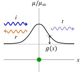
Our main assumption is that we can describe the response of graphene by a local conductivity . This assumption is readily justified if the density and the chemical potential of graphene are smoothly varying, see Fig. 8. Thus, if the plasmon energy is much smaller than everywhere, is given by [Eq. (5) of the main text],
| (47) |
Here is the Drude weight and the dimensionless function is the phenomenological damping rate. We assume that the system remains uniform in the -direction at all . The legitimacy of the local conductivity approximation is less obvious if the carrier density varies sharply, e.g., in a box-like fashion depicted in Fig. 6(c). However, it should be indeed valid in the context of the plasmon propagation if the plasmon wavelength is longer than the characteristic length scale of nonlocality (the Fermi wavelength or the characteristic width of the inhomogeneity, whichever is larger). The effective local conductivity can then be defined by averaging the nonlocal one over a suitable interval , see Eq. (40). In this case, Eq. (47) should be considered a formal parametrization of function . In particular, should be understood as damping averaged over the lengthscale .
Let us suppose that at , and approach constant values and , respectively and let us define the dimensionless function
| (48) |
If were constant, this function would be equal to , see Fig. 8.
We want to study how an incident plasmon plane wave with momentum is scattered by the inhomogeneity. We will show that the corresponding reflection coefficient is given by the formula
| (49) |
where
| (50) |
In particular, for normal incidence, , , the reflection coefficient is
| (51) |
similar to the usual first Born approximation. Note that because of the translational invariance in , the momentum is conserved.
Let us outline the derivation. Assuming , which is satisfied in our experiment, we can neglect retardation and treat the problem in the quasistatic approximation. As our main dependent variable we choose the electric potential . In general, is the sum of the external potential and the potential induced by charge density in graphene,
| (52) |
where is the Coulomb kernel and the asterisk denotes convolution,
| (53) |
Combining together these equations plus the continuity equation for current and charge density, we obtain
| (54) |
For an ideal uniform sample the solution of this equation has the form of a Fourier integral:
| (55) |
The zero of the dielectric function defines the plasmon momentum
| (56) |
introduced in the main text. The momentum is complex for any finite damping, , with having the physical meaning of the inverse propagation length. Indeed, in the absence of the external potential, one can find (unbounded) solutions with real and complex , , which can be thought of as decaying plane waves that are incident from the far left at some oblique angle. In the problem we study graphene is inhomogeneous, is -dependent,
| (57) |
and so the solution would contain the incident and the scattered (reflected plus transmitted) waves, see Fig. 8.
Setting and in Eq. (54), we obtain the equation for :
| (58) |
Here is the 1D Coulomb kernel and is the modified Bessel function of the second kind. Using the Green’s function
| (59) |
we find the equation for the scattered wave :
| (60) |
We expect at large negative , which implies
| (61) |
To the first order in the small parameter we can replace with in the integral, which leads to Eqs. (49). A particularly simple result is obtained if the plasmon wavelength
| (62) |
is much larger than the characteristic width of the inhomogeneity, in which case . Using Eqs. (47) and (51), we find the reflection coefficient
| (63) |
for the normal incidence. This simple equation gives a basic idea how may depend on and the local change in .
Appendix D Fitting the near-field profiles
As described in the main text, the near-field amplitude and phase measured in our imaging experiments reveals the presence of interference fringes, i.e., spatial modulations near the nanotube. For example, variations of are seen in Fig. 4(e) of the main text. Assuming these relative modulations should be of the order of the plasmon reflection coefficient , we can use Eq. (63) to estimate the perturbation of the conductivity caused by the nanotube. Using the representative value of at frequency at which the effective permittivity is equal to
| (64) |
we find from Eq. (56). Hence, we can reproduce if we assume, for example, that the reactive part of the conductivity is constant, while the dissipative part is enhanced to about over an interval of width near the origin. These numbers are generally consistent with the estimates in the main text.
To go beyond such rough estimates, additional modeling is required. For it to be more realistic, several important issues need to be accounted for. First, the plasmon waves launched and detected by the s-SNOM tip are not simple plane waves because the tip is positioned very close to the nanotube. Second, the intensity of such waves depends in a nontrivial way on the electric field concentration that occurs inside the tip-sample nanogap. Third, in the experiment the tip-sample distance is varying periodically with the tapping frequency . The complex near-field amplitude corresponds to the signal demodulated at the third harmonic . The normalized signal is the ratio , where is a coordinate point giving a fair approximation of the limit. [ in Fig. 4(d)-(e) of the main text.] Because of these complications, the quantitative modeling of and is possible only through numerical simulations.
Previously, an electromagnetic solver was developed, Fei et al. (2012, 2013) which takes these issues into account. The algorithm implemented in the solver Fei et al. (2013) finds a numerical solution of Eq. (54) discretized on a double grid of and . The external field is taken to be the sum of two terms. The first one, a constant, represents the incident infrared beam. The second one approximates the field created by the tip, modeled as an elongated metallic spheroid. The charge density distribution on the spheroid surface is found self-consistently from the condition that this surface is an equipotential. The total dipole moment of the tip, which represents the instantaneous amplitude of the scattered electromagnetic field is computed. Finally, is calculated by taking the appropriate Fourier transform and normalized to the reference point in order to yield and . The calculation is repeated for each tip position along the -axis.
Using this solver we were able to produce simulated near-field profiles that matched well the measured ones using a set of adjustable parameters. We will now describe this fitting procedure and the results, Figs. 9 and 10. As explained in Appendix C, these fitting results should be considered an estimate of the nonlocal conductivity of graphene averaged over the lengthscale .
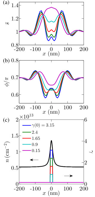
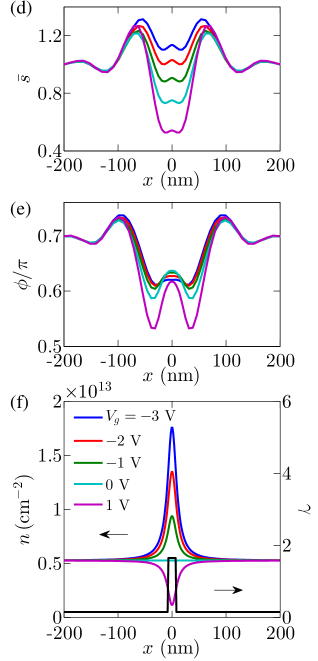
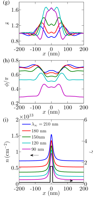
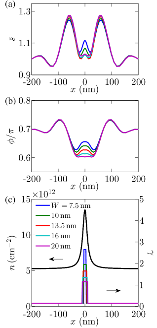
We took the trial damping function to be
| (65) |
where is the step-function, see the colored boxes in Fig. 9(c). For the carrier density profile we assumed the Lorentzian form [Fig. 9(c), black curve]
| (66) |
where is the graphene-nanotube distance and is the capacitance (per unit length) between them,
| (67) |
The effective static permittivity of the dielectric environment around the nanotube is
| (68) |
Equation (66) for is appropriate for our relatively highly doped () graphene which screens the electric field of the nanotube like a good metal. Jiang and Fogler (2015) We have not measured the radius of the nanotube directly, so there is an uncertainty in . This uncertainty is however small due to the logarithmic form of . On the other hand, the voltage difference between the nanotube and graphene is measured. Hence, our model contains four adjustable parameters: , , , and . Instead of the last of these we can use the asymptotic plasmon wavelength because they are directly related via Eqs. (47), (56), (62), and one more equation,
| (69) |
A brief comment on the trial form of and may be in order. The discontinuous box-like profile of the dimensionless damping rate may seem artificial; however, since the plasmon wavelength is much larger than the width of the box , the near-field amplitude is largely insensitive to the precise functional form of . In principle, we could also choose a box-like profile for . However, Eq. (66) is just as convenient and is better physically motivated.
In Fig. 9(a, b) we show the simulated profiles of the near-field amplitude and phase for several ’s for fixed , , and . The profiles for and match those measured in the experiment rather well. This fitting suggests that the electrified nanotube causes the density change by almost a factor of three and the damping enhancement by more than an order of magnitude. The former conclusion should be robust as it is a consequence of the simple electrostatics. On the other hand, the latter should be considered the experimental discovery. An explanation for this surprisingly high local damping was presented in the main text and the technical details were given in Appendix A.
A rough correspondence between the numbers obtained above and the parameters of the square-well model can be established as follows. The depth of the well is taken as the integrated potential divided by the width of the well, . The potential can be found through and Eq. (69). This results in the dimensionless well depth . The estimation of the integrated conductivity is more complicated. Due to the presence of a nonzero background , density variations will also contribute to the real part of the optical conductivity. To isolate the contribution of the optical transitions, the integrated conductivity is calculated as , where is the conductivity of a comparison system, which has the same density profile but the constant damping rate . This prescription yields .
The dependence of and profiles on the other adjustable parameters, such as , , and also on the gate voltage is illustrated in Fig. 10(a, b), (g, h), and (d, e), respectively. The profiles vary dramatically with the changes in these parameters, and so the determination of the best-fitting values of the adjustable parameters has very little uncertainty. This analysis is yet another illustration of how the s-SNOM nanoimaging can be a powerful and sensitive technique for probing the local surface conductivity of graphene and perhaps many other 2D materials as well.
Appendix E Device Fabrication
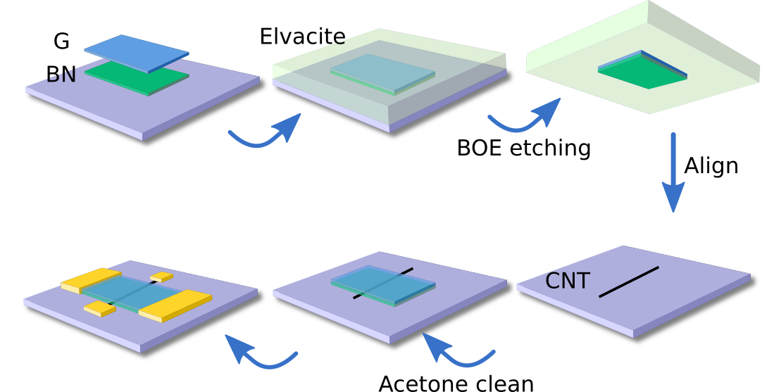
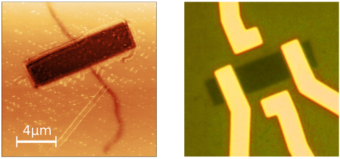
Our device consists of (from top to bottom) a graphene monolayer, a -thick hBN flake, a metallic single-wall CNT, and a SiO2/Si substrate. The CNT was grown by chemical vapor deposition, located using a scanning electron microscope, and transferred onto a SiO2/Si substrate. Monolayer graphene was mechanically exfoliated. Using a PPC/PDMS stamp, the graphene/hBN stack was transferred onto a separate SiO2/Si substrate. The stack was then picked up with an acrylic resin Elvacite Huang et al. (2015). It was subject to buffered oxide etch (BOE), aligned, and transferred to cover the CNT. The Elvacite was cleaned away with acetone. The final step of the fabrication was adding metallic contacts to the CNT and graphene. These steps are summarized in Fig. 11 (top). The AFM and optical images of the device are shown in Fig. 11 (bottom left and right).
Appendix F Supercritical transitions
Our problem has an intriguing parallel to the collapse of superheavy atoms in nuclear physics, which is as follows. For a very large nuclear charge , the extrapolated values of the first few atomic levels sink below the top of the positron energy band, Zeldovich and Popov (1972) , see Fig. 12(a). (Here is the fine-structure constant and is the electron mass.) Such supercritical states can no longer be bound to the nucleus but should be quasi-bound, being hybridized with the extended states in the positron band. In graphene where the role of is played by the Fermi velocity , the critical charge is rather small, Shytov et al. (2007b); Pereira et al. (2007). This has made it possible to observe the long-sought supercriticality experimentally by measuring the tunneling density of states near charged impurities Wang et al. (2013). Analogous transitions Kennedy (2002) are possible for the bound states studied in this Letter, Fig. 12(b). Compared to prior studies of a single Shytov et al. (2007b); Pereira et al. (2007); Fogler et al. (2007) or a few pointlike charges Wang et al. (2013); Pereira et al. (2007); De Martino et al. (2014); Gorbar et al. (2015), the 1D geometry examined in this work has several advantages. The gapless 2D Dirac spectrum is replaced by a gapped one with [Fig. 12(b)], making the analogy to the atomic collapse problem Zeldovich and Popov (1972) closer. Alternatively, it prompts an analogy to a hypothetical cosmic string Nascimento et al. (1999), previously used in graphene literature Pereira et al. (2010); Chakraborty et al. (2013) in a different context. More importantly, our “1D atom” permits continuous in situ tunability in terms of at least two parameters: the gate voltage and the optical excitation frequency. Experimental verification of these supercritical transitions can be attempted via two complementary approaches. One is to examine the changes in the LDOS. In fact, the detailed calculations of the LDOS presented in Appendix B were done exactly with such experiments in mind. The other approach is to look for abrupt drops in the local optical conductivity caused by the liquidation of the optical transitions, see Fig. 3(b) of the main text. Unfortunately, in either the conductivity or the LDOS, the supercritical signatures are very subtle compared to those of, say, van Hove singularities. Also, pinpointing these transitions requires an exhaustive search of the parameter space, which, for technical reasons, has not been possible in the devices we fabricated so far. Nevertheless, this can be an interesting and challenging problem for future work.
References
- Das Sarma et al. (2011) S. Das Sarma, S. Adam, E. H. Hwang, and E. Rossi, Rev. Mod. Phys. 83, 407 (2011).
- Kotov et al. (2012) V. N. Kotov, B. Uchoa, V. M. Pereira, F. Guinea, and A. H. Castro Neto, Rev. Mod. Phys. 84, 1067 (2012).
- Basov et al. (2014) D. N. Basov, M. M. Fogler, A. Lanzara, F. Wang, and Y. Zhang, Rev. Mod. Phys. 86, 959 (2014).
- Principi et al. (2014) A. Principi, M. Carrega, M. B. Lundeberg, A. Woessner, F. H. L. Koppens, G. Vignale, and M. Polini, Phys. Rev. B 90, 165408 (2014).
- Woessner et al. (2014) A. Woessner, M. B. Lundeberg, Y. Gao, A. Principi, P. Alonso-González, M. Carrega, K. Watanabe, T. Taniguchi, G. Vignale, M. Polini, J. Hone, R. Hillenbrand, and F. H. L. Koppens, Nature Mater. 14, 421 (2014).
- Jablan et al. (2009) M. Jablan, H. Buljan, and M. Soljačić, Phys. Rev. B 80, 245435 (2009).
- Vakil and Engheta (2011) A. Vakil and N. Engheta, Science 332, 1291 (2011).
- Grigorenko et al. (2012) A. N. Grigorenko, M. Polini, and K. S. Novoselov, Nature Photon. 6, 749 (2012).
- García de Abajo (2014) F. J. García de Abajo, ACS Photon. 1, 135 (2014).
- Kechedzhi and Das Sarma (2013) K. Kechedzhi and S. Das Sarma, Phys. Rev. B 88, 085403 (2013).
- Garcia-Pomar et al. (2013) J. L. Garcia-Pomar, A. Y. Nikitin, and L. Martin-Moreno, ACS Nano 7, 4988 (2013).
- Fei et al. (2013) Z. Fei, A. S. Rodin, W. Gannett, S. Dai, W. Regan, M. Wagner, M. K. Liu, A. S. McLeod, G. Dominguez, M. Thiemens, A. H. Castro Neto, F. Keilmann, A. Zettl, R. Hillenbrand, M. M. Fogler, and D. N. Basov, Nature Nano. 8, 821 (2013).
- Schnell et al. (2014) M. Schnell, P. S. Carney, and R. Hillenbrand, Nature Comm. 5, 3499 (2014).
- Ju et al. (2015) L. Ju, Z. Shi, N. Nair, Y. Lv, C. Jin, J. Velasco, C. Ojeda-Aristizabal, H. A. Bechtel, M. C. Martin, A. Zettl, J. Analytis, and F. Wang, Nature 520, 650 (2015).
- Kennedy (2002) P. Kennedy, J. Phys. A 35, 689 (2002).
- Hartmann and Portnoi (2014) R. R. Hartmann and M. E. Portnoi, Phys. Rev. A 89, 012101 (2014).
- Candemir and Bayrak (2013) N. Candemir and O. Bayrak, J. Math. Phys. 54, 042104 (2013).
- Villalba and Greiner (2003) V. M. Villalba and W. Greiner, Phys. Rev. A 67, 052707 (2003).
- (19) See Appendix for the calculation of , , and the s-SNOM data analysis.
- Beenakker et al. (2009) C. W. J. Beenakker, R. A. Sepkhanov, A. R. Akhmerov, and J. Tworzydło, Phys. Rev. Lett. 102, 146804 (2009).
- Ni et al. (2015) G. X. Ni, H. Wang, J. S. Wu, Z. Fei, M. D. Goldflam, F. Keilmann, B. Özyilmaz, A. H. Castro Neto, X. M. Xie, M. M. Fogler, and D. N. Basov, Nature Mater. 14, 1217 (2015).
- Keilmann and Hillenbrand (2009) F. Keilmann and R. Hillenbrand, “Nano-optics and Near-field Optical Microscopy,” (Artech House, Norwood, 2009) Chap. 11: Near-Field Nanoscopy by Elastic Light Scattering from a Tip, pp. 235–266, edited by A. Zayats and D. Richards.
- Atkin et al. (2012) J. M. Atkin, S. Berweger, A. C. Jones, and M. B. Raschke, Adv. Phys. 61, 745 (2012).
- Fei et al. (2012) Z. Fei, A. S. Rodin, G. Andreev, W. Bao, A. S. McLeod, M. Wagner, L. Zhang, Z. Zhao, M. Thiemens, G. Dominguez, M. M. Fogler, A. H. Castro Neto, C. Lau, F. Keilmann, and D. N. Basov, Nature 487, 82 (2012).
- Chen et al. (2012) J. Chen, M. Badioli, P. Alonso-Gonzalez, S. Thongrattanasiri, F. Huth, J. Osmond, M. Spasenovic, A. Centeno, A. Pesquera, P. Godignon, A. Zurutuza Elorza, N. Camara, F. J. García de Abajo, R. Hillenbrand, and F. H. L. Koppens, Nature 487, 77 (2012).
- Jiang and Fogler (2015) B.-Y. Jiang and M. M. Fogler, Phys. Rev. B 91, 235422 (2015).
- Dai et al. (2014) S. Dai, Z. Fei, Q. Ma, A. S. Rodin, M. Wagner, A. S. McLeod, M. K. Liu, W. Gannett, W. Regan, M. Thiemens, G. Dominguez, A. H. Castro Neto, A. Zettl, F. Keilmann, P. Jarillo-Herrero, M. M. Fogler, and D. N. Basov, Science 343, 1125 (2014).
- Shi et al. (2015) Z. Shi, X. Hong, H. A. Bechtel, B. Zeng, M. C. Martin, K. Watanabe, T. Taniguchi, Y.-R. Shen, and F. Wang, Nature Photon. 9, 515 (2015).
- Giles et al. (2016) A. J. Giles, S. Dai, O. J. Glembocki, A. V. Kretinin, Z. Sun, C. T. Ellis, J. G. Tischler, T. Taniguchi, K. Watanabe, M. M. Fogler, K. S. Novoselov, D. N. Basov, and J. D. Caldwell, Nano Lett. XX, XXX (2016).
- (30) Z. Fei, M. Scott, D. J. Gosztola, J. J. Foley, J. Yan, D. G. Mandrus, H. Wen, P. Zhou, D. W. Zhang, Y. Sun, J. R. Guest, S. K. Gray, W. Bao, G. P. Wiederrecht, and X. Xu, “Nano-optical imaging of exciton polaritons inside WSe2 waveguides,” arXiv:1601.02133.
- Wunsch et al. (2006) B. Wunsch, T. Stauber, F. Sols, and F. Guinea, New J. Phys. 8, 318 (2006).
- Wang et al. (2013) Y. Wang, D. Wong, A. V. Shytov, V. W. Brar, S. Choi, Q. Wu, H.-Z. Tsai, W. Regan, A. Zettl, R. K. Kawakami, S. G. Louie, L. S. Levitov, and M. F. Crommie, Science 340, 734 (2013).
- Shytov et al. (2007a) A. V. Shytov, M. I. Katsnelson, and L. S. Levitov, Phys. Rev. Lett. 99, 246802 (2007a).
- Huang et al. (2015) J.-W. Huang, C. Pan, S. Tran, B. Cheng, K. Watanabe, T. Taniguchi, C. N. Lau, and M. Bockrath, Nano Lett. 15, 6836 (2015).
- Zeldovich and Popov (1972) Y. B. Zeldovich and V. S. Popov, Sov. Phys. Uspekhi 14, 673 (1972).
- Shytov et al. (2007b) A. V. Shytov, M. I. Katsnelson, and L. S. Levitov, Phys. Rev. Lett. 99, 236801 (2007b).
- Pereira et al. (2007) V. M. Pereira, J. Nilsson, and A. H. Castro Neto, Phys. Rev. Lett. 99, 166802 (2007).
- Fogler et al. (2007) M. M. Fogler, D. S. Novikov, and B. I. Shklovskii, Phys. Rev. B 76, 233402 (2007).
- De Martino et al. (2014) A. De Martino, D. Klöpfer, D. Matrasulov, and R. Egger, Phys. Rev. Lett. 112, 186603 (2014).
- Gorbar et al. (2015) E. V. Gorbar, V. P. Gusynin, and O. O. Sobol, Phys. Rev. B 92, 235417 (2015).
- Nascimento et al. (1999) J. R. S. Nascimento, I. Cho, and A. Vilenkin, Phys. Rev. D 60, 083505 (1999).
- Pereira et al. (2010) V. M. Pereira, A. H. Castro Neto, H. Y. Liang, and L. Mahadevan, Phys. Rev. Lett. 105, 156603 (2010).
- Chakraborty et al. (2013) B. Chakraborty, K. S. Gupta, and S. Sen, J. Phys. Conf. Ser. 442, 012017 (2013).