Determining graphene’s induced band gap with magnetic and electric emitters
Abstract
We present numerical and analytical results for the lifetime of emitters in close proximity to graphene sheets. Specifically, we analyze the contributions from different physical channels that participate in the decay processes. Our results demonstrate that measuring the emitters’ decay rates provides an efficient route for sensing graphene’s optoelectronic properties, notably the existence and size of a potential band gap in its electronic bandstructure.
pacs:
81.05.ue,78.67.Wj,73.20.Mf,13.40.HqDriven by its successful isolation, graphene has not stopped fascinating the research community. Although, this allotropic form of carbon had been theoretically investigated for decades, experimental access to graphene has offered new perspectives as well as novel directions for fundamental research and technological applications Geim07 ; Geim09 . Graphene’s exotic properties Castro-Neto09 have lead to the investigation of a wide range of phenomena such as ballistic transport Bae13 , the quantum Hall effect Geim07 ; Novoselov07 , and thermal Balandin11 as well as electrical conductivity Wunsch_2006 ; Guo11 . Developing a detailed understanding, followed by appropriate engineering of these properties, lies at the heart of future graphene-based technologies. For this, an accurate determination of graphene’s properties in realistic experimental settings and the detailed validation of various theoretical models (cf. Ref Wunsch_2006 ; Hwang_2007 ; Bordag_2014 ; Bordag_2015 ) is indispensable. Promising designs where the semi-metal will play an important role, aim at combining condensed-matter with atomic systems. Such hybrid devices are geared towards reaping the best of the two worlds for advanced high-performance devices.
In this work, we demonstrate how the high degree of control and accuracy available in quantum systems like cold atoms and Si- and NV-centers in nano-diamonds, can be employed for detailed investigations of graphene’s optoelectronic properties Gomez-Santos_2011 ; Nikitin_2011 ; Tielrooij15 ; Kort_2015 . Specifically, we focus on modifications in the life times of emitters held in close proximity of graphene layers and show that these allow for direct experimental access to features like band gaps as well as plasmons and/or plasmon-like resonances. In graphene, a band gap (cf. Fig. 1) is created (i) when the atomically thin material is deposited on a substrate Giovannetti07 ; Jung_2015 , (ii) when strain is applied, (iii) when impurities are present, and (iv) in cases where graphene bilayers instead of a single layer are considered. Values for of the order of tens of meV have been predicted Giovannetti07 ; Jung_2015 , thus triggering corresponding experimental investigations. These band gaps and the features connected with them are still the subject of discussions Bai_2015 ; Kumar_2015 so that reliable experimental means for their analysis are highly desirable.
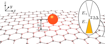
For planar geometries the decay rate of an emitter is a functional of the system’s optical scattering coefficients. We model a monoatomic graphene layer in terms of a 2+1-dimensional Dirac fluid Fialkovsky_2011 ; Chaichian_2012 ; Bordag_2014 and embed it in a non dispersive and non dissipative dielectric medium with permittivity . As a result, the graphene layer is characterized by an induced band gap and a chemical potential (cf. Fig. 1) while the corresponding electromagnetic reflection coefficients for transverse magnetic (TM) and transverse electric (TE) waves are Fialkovsky_2011 ; Chaichian_2012
| (1) |
where is the fine structure constant and
| (2) |
with . Further, and denote, respectively, the moduli of the out-of-plane and in-plane wave vectors in the dielectric medium. In addition, we use dimensionless variables, which amounts to the replacements , , and ( for graphene). Life time modifications are usually associated with the strength of scattering processes. Owing to its minute thickness (few Å), the optical response of a single graphene layer is rather small ( reflection Nair_2008 ). Thus, for emitters near a graphene layer, small life time modifications might naively be expected. However, graphene’s exotic properties introduce additional features that affect the emitters’ dynamics, such as TE plasmons and single (SPE)- and multiple (MPE)-particle excitations.
Different frequencies are associated with the different physical processes: propagating fields occur for and evanescent fields are characterized by . Further, we identify another regime where , which only exists if ,i.e., if the radiation frequency exceeds that associated with the band gap. In this regime, the 2+1-dimensional Dirac fluid model of graphene features the creation of electron-hole pairs. In the propagating regime, the scattering process in graphene systems is very similar to that in ordinary thin films. This similarity, however, already breaks down for evanescent waves, for which the scattering process is associated with surface plasmons or plasmon-like phenomena: While in ordinary materials these resonances are usually present only in TM polarization, graphene is known for admitting such excitations in both TM and TE polarization Mikhailov_2007 ; Bordag_2014 ; Stauber_2014 ; Bordag_2015 . TM polarized surface plasmons are associated with charge density oscillations and are dominated by the electric field. Conversely, TE plasmons result from resonances in the motion of the current density so that they are dominated by the magnetic field. Mathematically, these phenomena are related to divergences of the scattering coefficients and in our case they can be investigated by analyzing the poles of Eqs. (1). In our model TM plasmons do not occur, while the TE plasmon’s dispersion relation reads as
| (3) |
where . This agrees well with previous numerical results for vacuum () Bordag_2014 .
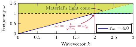
Albeit difficult to discern in Fig. 2, Eq. (3) indicates that the TE plasmon’s dispersion relation lies exclusively in the evanescent region and stays outside of the single-particle excitation region (SPE) TE-Plasmon-Paper-auf-ArXiV . Two distinct characterstics become apparent: For low frequencies (), the dispersion curve lies close to but below the medium’s light cone; For large frequencies (), the properties of the TE plasmon’s dispersion do not depend on the embedding dielectric but are solely determined by graphene itself.
With respect to the processes described above, the total decay rate of an emitter with dipole operator can be written as where is the decay rate in a homogeneous dielectric without graphene. The factor indicates the usually frequency-dependent local field correction one has to take into account to correctly describe the dynamics of an emitter embedded in a dielectric ( for ) Glauber91 ; Intravaia15a . For simplicity, we will not dwell on this issue and instead refer readers to the literature for further information Glauber91 ; Intravaia15a ; Scheel99 ; Vries98 . The functions are related to the matrix elements of the orthogonal and parallel components of the dipole with respect to the graphene layer (). In turn, each of these two contributions is the result of the three processes discussed above. Consequently, we have a the radiative term , which originates from the propagating region (including the radiative part of the SPE region), the contribution of the (non-radiative) SPE region , and the non-radiative contribution given by plasmonic excitations .
In order to analyze the above terms in more detail, we will first discuss the case of magnetic decay keeping in mind that a magnetic emitter ought to be more sensitive to the magnetic field associated with plasmonic TE resonances. The emitter has a transition frequency and is located at above the graphene layer at (see Fig. 1). Within second-order perturbation theory Henkel_1999 ; Novotny_2012 the modification of the decay rate can be written as
| (4a) | ||||
| (4b) | ||||
Here, , . We have also defined and . In Eqs. (4), the evanescent contribution is associated with the range , while the corresponds to the propagating region. The SPE range corresponds to .
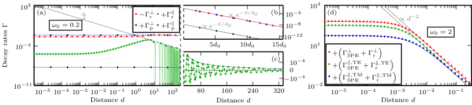
We first consider the contribution to the decay rate from the evanescent range, imputable only to the resonance in the reflection coefficients. In view of the above discussion of the dispersion relation, Eqs. (3), this contribution features two different regimes. For , i.e., when the dispersion curve is very close to the light cone, the resonance is located at . The leading terms of Eqs. (4) are then
| (5) |
Given the rather large characteristic decay length , these contribitions exhibit weak distance-dependencies for experimentally relevant emitter-graphene separations of a few microns. For , the resonance is instead located close to the boundary of the SPE region, and we obtain
| (6a) | ||||
| (6b) | ||||
Due to the small values of and , the above terms are strongly suppressed in graphene unless , which only occurs when .
For the same parameters, the propagating regime corresponds to a rather small integration range in Eqs. (4). Therefore, the integrands can be expanded around and after some rearrangements we obtain
| (7a) | ||||
| (7b) | ||||
Interestingly, because of the overall minus sign of , this contribution tends to increase the emitter’s life time, suppressing the decay process relative to . In addition, since , due to the dephasing between the propagating waves, exponentially decays for distances . It follows a behavior similar to the TE plasmon but with characteristic decay length . Therefore, since , is almost exactly canceled by (see Fig. 3(b)). For even larger distances (, not shown), due to the interference between incoming and scattered waves, oscillates in space like with a frequency (see Fig. 3(c)).
Finally, we consider the modification of the decay rate that stems from the SPE region. This contribution only occurs when the emitter’s transition frequency becomes larger than the electronic band gap (). Although, the total SPE region includes both evanescent and propagating contributions, the non-radiative part dominates at short distances and, as in the previous case, is almost constant for . Again, since , in this limit we can write
| (8) |
This demonstrates that varies non-monotonously with frequency and exhibits a maximum for , where it takes the value . At intermediate distances, the total (evanescent and propagating) SPE contribution decays as a power law, (see Fig. 3(d)). For , the propagating waves induce once again spatial oscillations with frequency (not shown).
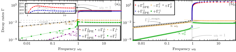
In Fig. 4(a) we present the frequency dependence of all the above-discussed contributions to the decay rate at a fixed distance from the graphene layer (corresponding to for an emitter with transition frequency of ). As discussed above, for emitters with transition frequencies smaller than graphene’s electronic band gap (), the two main decay channels are the TE plasmonic resonance and the radiative decay. Their relative importance differs, depending on the spatial orientation of the dipole-matrix elements. We see that in the plasmonic TE resonance provides an enhancement while the radiative contribution leads to a suppression. Also, over a very large range of frequencies. For , the radiative contribution dominates and leads to an enhancement of the decay rate. In this case, the plasmonic TE resonance, due to its proportionality to , represents a subleading contribution. For , the dominant contribution for both and stems from the SPE contribution (see Fig. 4(a), inset) and leads to an enhancement of the decay rate by three orders of magnitude. Note, that the increase of the decay rate occurs quite abruptly as the frequency of the emitter moves across the band gap and, for larger frequencies, takes on a weakly frequency-dependent value around . In both , the TE contributions are dominant and lead to the non-monotonic behavior discussed above.
Most of the above-described characteristics also qualitatively apply to the case of an electric dipole emitter (see Fig. 4(b)). Indeed, the relevant expressions can be easily obtained by swapping the reflection coefficients in Eqs. (4) Henkel_1999 ; Intravaia11 . For brevity we will only mention that, as a consequence of the replacement , some features are found in instead of . Curiously, for , due to the proximity of the TE plasmon dispersion relation to the light cone, its contribution to the decay rate is of the same order of magnitude for both emitters and for all distances, i.e., . More importantly, the SPE channel still provides a large enhancement of the decay rate for , featuring again a quite abrupt jump for frequencies near the electronic band gap of graphene. However, for the electric emitter both exhibit a monotonous frequency dependence.
In conclusion, the above results suggest atomic or atom-like emitters as sensitive quantum probes to determine the physical properties of graphene and, in particular, to investigate a band gap in its electronic bandstructure. Using these systems allows for an accurate analysis of this quantity, especially in complex (but relevant for graphene-based technologies) situations where it is no longer spatially homogenous: This occurs, e.g., when the sheet (i) is exposed to mechanical stress Zhu15 , (ii) is positioned on an inhomogeneous substrate or (iii) absorbs impurities (in a controlled Elias09 or uncontrolled fashion). In our approach, the emitter non-invasively probes graphene’s properties in different physical regimes, enabling experimental investigation of unusual graphene properties such as TE surface resonances (see also Gomez-Santos_2011 ; Nikitin_2011 ) and providing results complementary to those accessible when using other procedures. In addition, the possibility to engineer different internal quantum states of the emitter and study their lifetimes can also offer new opportunities which are presently not accessible with other techniques. As a concrete experimental approach, we suggest to extending the known use of microtrapped Bose-Einstein condensates Wildermuth_2005 ; Wildermuth_2006 to map the local band gap structure of graphene sheets with micron resolution. One would detect the splin flip rate by measuring the spatially dependent spin population after a known time since its preparation as a spin-polarized gas. For enhanced sensitivity, it will be advantageous to employ an optical dipole trap, ideally configured as a light sheet, tuned to a frequency below the main atomic transition. Fluorescence imaging following selective resonant excitation of the emitter decay target state will enable the measurement of even very slow decay rates down to a few events per time across the ensemble of typically atoms. The high temporal resolution of this technique can offer an important advantage in analyzing the different (relatively slow) processes cited above.
In addition to atomic quantum gases other very well suited candidates are Si- and NV-centers in nano-diamonds. They do not only show tunable magnetic and electric transitions from the MHz to the THz frequency range but also simultaneously allow for high position resolution Schell_2014 . Small band gaps can be investigated by cooling the system to the mK regime, such that magnetically tunable Zeeman Amsuss_2011 or hyperfine transitions Tkalcec_2014 can be utilized. Our work can open additional pathways to enhance the fundamental understanding of the validity of different graphene models Stauber_2014 ; Roldan_2013 ; Brida_2013 and also provides relevant information for realistic applications and new designs of interest, e.g., in atom-chip research Folman02 ; Fortagh07 ; Sinuco-Leon11 . Indeed, this material with its intrinsic, room-temperature quantum properties Geim09 ; Novoselov07 ; Tombros_2007 has been deemed as a particularly interesting addition to these systems in order to proceed further on the road to quantum computing Trauzettel_2007 ; Guo_2009 .
Acknowledgements.
We thank Ch. Koller, M. T. Greenaway and T. M. Fromhold for stimulating discussions. We acknowledge support by the Deutsche Forschungsgemeinschaft (DFG) through the Collaborative Research Center (CRC) 951 “Hybrid Inoganic/Organic Systems for Optoelectronics (HIOS)” within Project No. B10. P.K. acknowledges support from EPSRC (grant EP/K03460X). F.I. further acknowledges financial support from the EU through the Career Integration Grant No. PCIG14-GA-2013-631571 and from the DFG through the DIP Program (No. FO 703/2-1).
References
- (1) A. K. Geim and K. S. Novoselov, Nature Mater. 6, 183 (2007).
- (2) A. K. Geim, Science 324, 1530 (2009).
- (3) A. H. Castro Neto, F. Guinea, N. M. R. Peres, K. S. Novoselov, and A. K. Geim, Rev. Mod. Phys. 81, 109 (2009).
- (4) M.-H. Bae, Z. Li, Z. Aksamija, P. N. Martin, F. Xiong, Z.-Y. Ong, I. Knezevic, and E. Pop, Nature Comm. 4, 1734 (2013).
- (5) K. S. Novoselov, Z. Jiang, Y. Zhang, S. V. Morozov, H. L. Stormer, U. Zeitler, J. C. Maan, G. S. Boebinger, P. Kim, and A. K. Geim, Science 315, 1379 (2007).
- (6) A. A. Balandin, Nature Mater. 10, 569 (2011).
- (7) B. Wunsch, T. Stauber, F. Sols, and F. Guinea, New J. Phys. 8, 318 (2006).
- (8) B. Guo, L. Fang, B. Zhang, and J. R. Gong, Insciences J. 1, 80 (2011).
- (9) E. H. Hwang and S. DasSarma, Phys. Rev. B 75, 205418 (2007).
- (10) M. Bordag and I. G. Pirozhenko, Phys. Rev. B 89, 035421 (2014).
- (11) M. Bordag and I. G. Pirozhenko, Phys. Rev. D 91, 085038 (2015).
- (12) G. Gómez-Santos and T. Stauber, Phys. Rev. B 84, 165438 (2011).
- (13) A.Y. Nikitin, F. Guinea, F.J Garcia-Vidal and L. Martin-Moreno. Phys. Rev. B 84 195446 (2011).
- (14) W. J. M. Kort-Kamp, B. Amorim, G. Bastos, F. A. Pinheiro, F. S. S. Rosa, N. M. R. Peres,and C. Farina, Phys. Rev. B 92, 205415 (2015).
- (15) K. J. Tielrooij, L. Orona, A. Ferrier, M. Badioli, G. Navickaite, S. Coop, Nature Phys. 11, 281 (2015).
- (16) G. Giovannetti, P. A. Khomyakov, G. Brocks, P. J. Kelly, and J. van den Brink, Phys. Rev. B 76, 073103 (2007).
- (17) J. Jung, A. M. DaSilva, A. H. MacDonald, and S. Adam, Nat. Commun. 6, 6308 (2015).
- (18) K.-K. Bai, Y. C. Wei, J. B. Qiao, S. Y. Li, L. J. Yin, W. Yan, J. C. Nie, and L. He, Phys. Rev. B 92, 121405 (2015).
- (19) A. Kumar, A. Nemilentsau, K. H. Fung, G. Hanson, N. X. Fang, and T. Low, Phys. Rev. B 93, 041413R (2016).
- (20) I. V. Fialkovsky, V. N. Marachevsky, and D. V. Vassilevich, Phys. Rev. B 84, 035446 (2011).
- (21) M. Chaichian, G. L. Klimchitskaya, V. M. Mostepanenko, and A. Tureanu, Phys. Rev. A 86, 012515 (2012).
- (22) J. F. M. Werra, F. Intravaia, and K. Busch, J.Opt. 18, 034001 (2016).
- (23) R. J. Glauber and M. Lewenstein, Phys. Rev. A 43, 467 (1991).
- (24) F. Intravaia and K. Busch, Phys. Rev. A 91, 053836 (2015).
- (25) S. Scheel, L. Knöll, and D.-G. Welsch, Phys. Rev. A 60, 4094 (1999).
- (26) P. de Vries and A. Lagendijk, Phys. Rev. Lett. 81, 1381 (1998).
- (27) R. Nair, P. Blake, A. N. Grigorenko, K. S. Novoselov, T. J. Booth, T. Stauber, N. M. R. Peres, and A. K. Geim, Science 320, 1308 (2008).
- (28) S. A. Mikhailov and K. Ziegler, Phys. Rev. Lett. 99, 016803 (2007).
- (29) T. Stauber, J. Phys. - Condens. Mat. 26, 123201 (2014).
- (30) C. Henkel, S. Pötting, and M. Wilkens, Appl. Phys. B 69, 379 (1999).
- (31) L. Novotny and B. Hecht, Principles of Nano-Optics, 2nd ed. (Cambridge University Press, New York, 2012).
- (32) F. Intravaia, C. Henkel, and M. Antezza, in Casimir Physics, Vol. 834 of Lecture Notes in Physics, edited by D. Dalvit, P. Milonni, D. Roberts, and F. da Rosa (Springer, Berlin / Heidelberg, 2011), pp. 345–391.
- (33) S. Zhu, J. A. Stroscio, and T. Li, Phys. Rev. Lett. 115, 245501 (2015).
- (34) D. C. Elias, R. R. Nair, T. M. G. Mohiuddin, S. V. Morozov, P. Blake, M. P. Halsall, A. C. Ferrari, D. W. Boukhvalov, M. I. Katsnelson, A. K. Geim, and K. S. Novoselov, Science 323, 610 (2009).
- (35) S. Wildermuth, S. Hofferberth, I. Lesanovsky, E. Haller, L. M. Andersson, L Mauritz and S. Groth, I. Bar-Joseph, P. Krüger, and J. Schmiedmayer, Nature 435, 440 (2005).
- (36) S. Wildermuth, S. Hofferberth, I. Lesanovsky, S. Groth, P. Krüger, J. Schmiedmayer, and I. Bar-Joseph, Appl. Phys. Lett. 88, 264103 (2006).
- (37) A. W. Schell, P. Engel, J. F. M. Werra, C. Wolff, K. Busch, and O. Benson, Nano Lett. 14, 2623 (2014).
- (38) R. Amsüss, Ch. Koller, T. Nöbauer, S. Putz, S. Rotter, K. Sandner, S. Schneider, M. Schramböck, G. Steinhauser, H. Ritsch, J. Schmiedmayer, and J. Majer, Phys. Rev. Lett. 107, 060502 (2011).
- (39) A. Tkalc̆ec, S. Probst, D. Rieger, H. Rotzinger, S. Wünsch, N. Kukharchyk, A. D. Wieck, M. Siegel, A. V. Ustinov, and P. Bushev, Phys. Rev. B 90, 075112 (2014).
- (40) R. Roldán, J.-N. Fuchs, and M. Goerbig, Solid State Commun. 175, 114 (2013).
- (41) D. Brida, A. Tomadin, C. Manzoni, Y. J. Kim, A. Lombardo, S. Milana, R. R. Nair, K. S. Novoselov, A. C. Ferrari, G. Cerullo, and M. Polini, Nature Commun. 4, 1987 (2013).
- (42) R. Folman, P. Krüger, J. Schmiedmayer, J. H. Denschlag, and C. Henkel, Adv. At. Mol. Opt. Phys. 48, 263 (2002).
- (43) J. Fortágh and C. Zimmermann, Rev. Mod. Phys. 79, 235 (2007).
- (44) G. Sinuco-León, B. Kaczmarek, P. Krüger, and T. M. Fromhold, Phys. Rev. A 83, 021401 (2011).
- (45) N. Tombros, C. Jozsa, M. Popinciuc, H. T. Jonkman, and B. J. Van Wees, Nature 448, 571 (2007).
- (46) B. Trauzettel, D. V. Bulaev, D. Loss, and G. Burkard, Nature Phys. 3, 192 (2007).
- (47) G.-P. Guo, Z.-R. Lin, T. Tu, G. Cao, X.-P. Li, and G.-C. Guo, New J. Phys. 11, 123005 (2009).