Laboratori Nazionali di Frascati dell’INFN. Università degli Studi Roma Tre, dipartimento di Fisica. \PACSes \PACSit29.40.Mc29.40.Vj
Performance study of single undoped CsI crystals for the Mu2e experiment
Sommario
The Mu2e experiment at Fermilab aims to measure the charged lepton flavor violating neutrinoless muon to electron conversion. The goal of the experiment is to reach a single event sensitivity of , to set an upper limit on the muon conversion rate at in a three years run. For this purpose, the Mu2e detector is designed to identify electrons from muon conversion and reduce the background to a negligible level. It consists of a low mass straw tracker and a pure CsI crystal calorimeter.
In this paper, the performance of undoped CsI single crystal is reported. Crystals from many vendors have been characterized by determining their Light Yield (LY) and Longitudinal Response Uniformity (LRU), when read with a UV extended PMT, and their time resolution when coupled to a Silicon Photomultiplier.
The crystals show a LY of 100 photoelectrons per MeV when wrapped with Tyvek and coupled to the PMT without optical grease. The LRU is well represented by a linear slope that is on average 0.6%/cm. Both measurements have been performed using a 22Na source.
The timing performance have been evaluated exploiting minimum ionizing particles, with MPPC readout. A timing resolution better than 400 ps is achieved (at 20 MeV).
1 Introduction
The Mu2e experiment [1] at Fermi National Accelerator Laboratory, will search for the charged lepton flavor violating (CLFV) process of muon conversion in an aluminum nucleus field, .
Mu2e measure the ratio, , between the muon conversion and the muon capture rates, by Al nucleus, with a single event sensitivity (SES) of . This corresponds to set an upper limit of:
improving four orders of magnitude the previous result from SINDRUM II [2].
The signature of this neutrinoless conversion process is a mono energetic electron, with an energy slightly lower than the muon rest mass ( 104.96 MeV).
The Standard Model predicted rate for this process is , so that, observation of these processes could be a clear evidence for New Physics.
2 The Mu2e Calorimeter
The Mu2e detector consists of a low mass straw tracker and a crystal calorimeter. Both are located inside the evacuated warm bore of the Detector Solenoid in a uniform 1 T magnetic field, that is surrounded by a cosmic ray veto.
The detector is designed to identify the 105 MeV/c electrons from muons conversion, reducing the background to a negligible level.
The calorimeter, located behind the tracker, has to provide information about energy, timing and position to validate the charged particle reconstructed by the tracker and perform a particle identification.
To reach the SES required by the experiment and also maximize the acceptance for MeV conversion electrons, a crystal calorimeter with an energy resolution of and a timing resolution better than 500 ps in the energy region around 100 MeV is required. Moreover, the Mu2e environment implies the use of solid-state photodetectors immune to the presence of the magnetic field.
The baseline calorimeter is composed by 1400 pure CsI crystals, distributed in two annular disks and readout by two silicon photomultipliers (SiPMs) each.
In this paper the tests done on the light yield (LY) and the longitudinal response uniformity (LRU) of single CsI crystals are reported. Moreover, the timing performance has also been evaluated for some crystals, by coupling them to a SiPM.
2.1 Pure Csi crystals
Undoped Cesium Iodide (CsI) is a slightly hygroscopic crystal with an emission maximum at 315 nm, characterized by a relatively short decay time of 20 - 30 ns [3]. Together to this fast component, a much slower component with a decay time of about 1 ms is present which represents less than 15% of the total light output. The intensity of this slow component depends on the purity of the crystal since contamination with certain elements tends to degrade the fast-to-total ratio. This contribution is practically negligible in our CsI samples.
2.2 Silicon Photomultiplier, MPPC
Due to the high magnetic field, the CsI crystals readout has to be made by high-gain solid-state photodetectors, such SiPMs.
SiPMs are photon-counting devices made by one planar matrix of several avalanche photodiode (APD) pixels of the same shape, dimension and construction features that are operated in Geiger mode, with an inverse polarization above the breakdown. Each pixel is coupled to a quenching resistor [4].
At the wavelength emission peak of pure CsI (315 nm) the UV extended Hamamatsu SiPM, called Multi-Pixel Photon Counter (MPPC) is a good choice for the Mu2e calorimeter. In particular, the performance of S13361 series MPPCs are under study. It allows precision measurements, using the TSV (Through Silicon Via) technology [6]. There is no wire bonding, so the package outline is very close to the MPPC array. The outer gap from active area edge to package edge is only 0.2 mm.
3 Tests on single pure CsI crystals coupled to a UV extended PMT
To test the crystal production quality, we have procured 13 samples of pure CsI crystals from different high quality producers: 2 from Opto Materials (Italy), 7 from ISMA (Ukraine) companies, both with a crystal dimension of cm3 and four additional longer crystals cm3 from ISMA. The measurements have been performed at the INFN National Laboratory of Frascati (LNF) using a dedicated station for crystals testing.
3.1 Experimental setup
To study the LY and LRU of each crystal, we have used a low intensity collimated 22Na source which irradiates the crystal in a region of few mm2. The 22Na source produces 511 keV electron-positron annihilation photons and it is placed between the crystals and a small tagging system, constituted by a () mm3 LYSO crystal, readout by a () mm2 MPPC.
One of the two back-to-back photons produced by the source is tagged by this monitor, while the second one is used to calibrate the crystal under test, which is readout by means of a 2” UV extended photomultiplier tube (PMT) from ET Enterprises. This PMT has a quantum efficiency of at 310 nm, which is the wavelength where the undoped CsI reaches the emission maximum. The whole system is inside a light tight black box.
The data acquisition system is composed by a trigger board, which starts recording events applying a threshold of 20 mV on the tag signal, and a CAEN DT5751 digitizer at 109 samples per second, which acquires both tag and test signals.
For each crystal, a longitudinal scan is done irradiating eight points, of 2 cm step from the readout system. In the scan, the source and the tag are moved together along the axis of the crystal under test. All crystals have been tested when wrapped with a reflector material, which covers both the four surfaces along the longitudinal axis and the side opposite to the readout system.
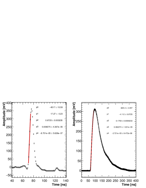
The digitizer has 1024 samples in the acquisition window, each sample corresponding to 1 ns. Examples of the pulse shapes, obtained for both tag and CsI crystals, are shown in Figure 1. The generic emission time distribution for a scintillator can be described as a fast component, generated by a two-step scintillation mechanism (absorption, emission) and a slow component [7]:
| (1) |
where , , are the time constants of the fast and slow scintillation process and of the rising part, respectively. is the ratio between the slow and the fast component. If we assume that the time resolution of our system can be described by a Gaussian, then the resulting distribution used to fit the waveforms is the convolution of with a Gaussian, as follows:
| (2) |
where:
| (3) |
is the error function, defined as:
| (4) |
and is the Gaussian standard deviation.
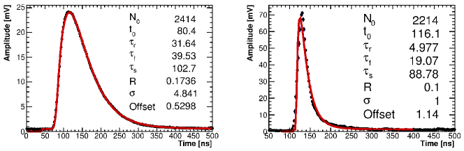
The profiles of the waveforms have been fit with Eq. 2 to evaluate the decay time of each crystal. Fit results are reported in Figure 1. Since CsI has a very small slow component, parameter has been fixed to 0.1, while the resolution function of our system has been set to ns. As shown in the same figure, in our setup, signals produced in CsI crystals are typically within 300 ns from the trigger, with a 50 ns delay offset, so that the charge is obtained integrating in the range () ns. The baseline is evaluated using the interval region above 700 ns.
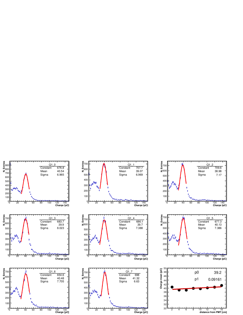
In Figure 2, the charge distributions for one of the crystals under test (Opto Materials 01), wrapped with Tyvek, are reported for the eight/one points of a single scan. The charge spectra are very clean and the peak due to the 511 keV photon is clearly visible. A Gaussian fit is applied to extract the mean values (): these values are then reported as a function of the distance of the source from the PMT, obtaining a linear slope parametrized as (Fig. 2, bottom right).
3.2 Light emission and longitudinal response uniformity performance
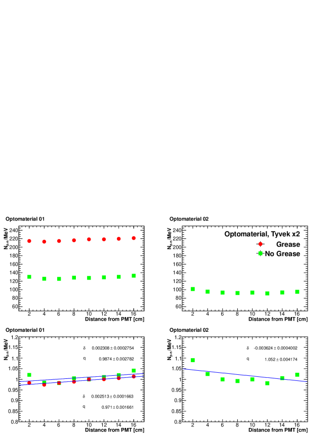
All crystals have been tested with the 22Na using just one orientation with respect to the readout system. For some of the crystals, the effect of the optical grease contact with the PMT has also been studied.
A reflector material wrapping is needed to improve the detection efficiency of scintillation photons. The Opto Materials pure CsI crystal number 02 has been tested with different wrapping materials: aluminum (Al), Tyvek, Teflon. The charge distributions have been fit with a gaussian function to extract the peak position and evaluate the LY, defined as the number of photoelectrons produced per MeV, :
| (5) |
where pC is the charge of the electron, keV is the energy of the annihilation photon and is the PMT gain.
The Al wrapping provided the worst LY (79 Np.e./MeV with the source in the central position), while the best performance, for every scan point, has been obtained with Teflon (91 Np.e./MeV) and Tyvek wrapping ( 89 Np.e./MeV), which provide a LY increase of a factor about 20% with respect to the configuration with Al. Therefore, tests on all the other crystals have been carried out with Tyvek wrapping, due to the fragility and difficulty to repair Teflon, especially when in presence of optical grease [5].
Examples of scan results are reported in Figure 3. In the top left figure, a comparison between optical grease and air coupling is also shown, an improvement of about 80% is clearly visible for all the scan points.
To summarize, tests on all the 13 crystals show that:
-
•
relevant differences between crystals from the same company exist. For instance, we observe a 45% better LY with Opto Materials sample 01 with respect to sample number 02 (Fig. 3);
-
•
similar performance for ISMA crystals, both long and short ones, and Opto Materials 02, while Opto Materials 01 has much better uniformity and LY (130 Np.e./MeV with respect to 100 Np.e./MeV);
-
•
larger signals are observed closer to the PMT, because of the collection of direct light;
-
•
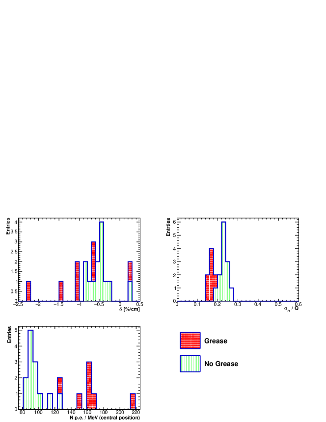
the charge resolution is 18% (25%) with (without) optical grease (Fig. 4).
To resume features of all the 13 crystals tested, the LY obtained with the source in the central scan position has been reported in Figure 4 (bottom left). To evaluate crystals LRU, the LY, normalized to its value in the central position, has been plotted as a function of the scan position and fit with a linear function (Fig. 3). Fits angular coefficients are reported in Figure 4, showing a LRU better than 0.5%/cm in most of the crystals.
4 Single channel Timing performance
A cm3 sample from each company, Opto Materials and ISMA, have been coupled to a SPL MPPC and tested with cosmic rays to evaluate the timing resolution.
4.1 Experimental setup
In order to optimize the light collection, crystals have been wrapped with 100 m-thick Tyvek foils, covering both the four faces along the crystal axis and the side opposite to the readout system. Each crystal has then placed between two small plastic scintillators, fingers, perpendicular to each other and positioned one below and one above the crystal under test. In this way, the two finger coincidence covers 1 cm2 area on the long surface of the crystal. For each crystal, the effect of the Rhodosil Paste 7 optical grease coupling has also been studied. The whole system has been assembled inside a light tight black box.
The data acquisition system is composed by a trigger board, that makes the coincidence between the two discriminated finger signals, and a CAEN DT5751 digitizer at 1 Giga samples per second, which acquires finger and crystal signals.
The goal of this test is to measure the time resolution achieved at the energy released by a minimum ionizing particle (MIP) in the crystal. In order to set the energy scale, we compare the charge spectra of the MIP with that from a radioactive source. Our 22Na source emits 511 keV back-to-back photons from annihilation and its charge spectrum has a corresponding mean value of () pC. For the cosmic rays charge plot, the most probable value is () pC. Comparing these two values, the energy released by a MIP in a crystal results to be around 20 MeV.
The amplifier used for the CR test was a prototype version with a gain of 3.
4.2 Timing analysis
Waveform examples obtained for one finger and for the crystal, are shown in Figure 5 (left and right respectively). To extract the time, the maximum value of pulse height for the finger and crystal signals has been evaluated and then a fit with a 4th order polynomial function has been performed between the times at two fixed thresholds: the position of the time sample corresponding to a pulse height of 10 mV above the signal baseline and the one at maximum pulse height less 1 ns ( - 1). The fit is shown in Figure 5.
Both for fingers and crystals the measured time is taken at a constant fraction CF, set at 25%, of the maximum signal amplitude. In order to eliminate the jitter due to the trigger, the half sum of the finger time has been subtracted:
| (6) |
where and are the time of the bottom and top fingers respectively and is the crystal time. The time jitter of the trigger, , is evaluated as the provided by the gaussian fit that is ps.
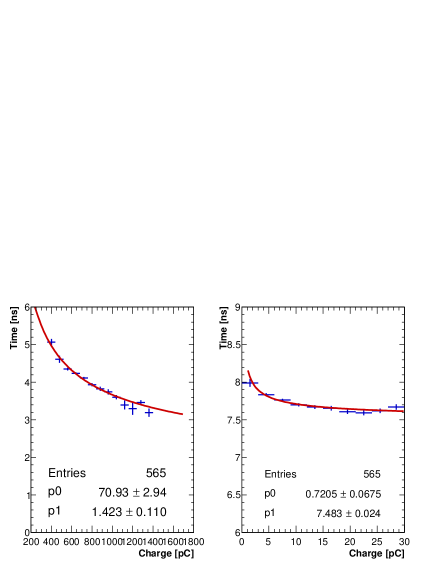
The detector timing properties are determined primarily by time slewing (or time walk) resulting from the signal rise time, shape and amplitude. The dependence of the time, , from the charge, , is shown in Figure 6. This behavior is described by the function:
| (7) |
where and are parameters evaluated by a fit to the dependence in FIg. 6 minimizing the .
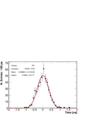
After the time slewing correction, the time distributions of the Opto Material 01 crystal tested, wrapped with Tyvek and Teflon and coupled with and without optical grease to the SPL MPPC, are reported in Figure 7. The time resolution, , is the ”Sigma” value of the gaussian fit, reported in the same figure.
 |
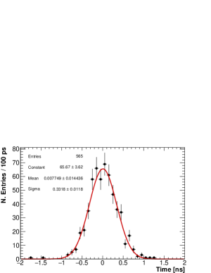 |
The best performance is obtained with optical grease coupling: () ps with Teflon and () ps with Tyvek wrapping. Coupling in air deteriorates the resolution: () ps with Teflon and () ps with Tyvek wrapping, as expexted by the loss of collected light. Then the time resolution after jitter subtraction is evaluated as:
| (8) |
In Table 1, all the jitter subtracted time resolutions obtained testing crystal + SPL MPPC exploiting cosmic rays are summarized.
| Tyvek | Tyvek and grease | Teflon | Teflon and grease | |
|---|---|---|---|---|
| Opto Materials 01 | 410 | 270 | 375 | 260 |
| Opto Materials 02 | - | 280 | - | - |
| ISMA 05 | - | 265 | - | - |
Another kind of Hamamatsu MPPCs with a different cover layer have also been tested. These are the so called Micro Film MPPCs.
In this final test, the time has been evaluated in a similar manner, by using two variable thresholds for the fit range (the fit function remains a 4th order polynomial) at respectively 0.1% and 85% of the signal maximum amplitude. These threshold values are obtained performing a scan and minimizing the time resolution.
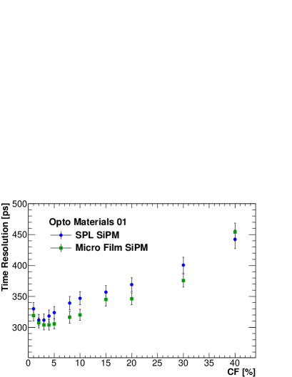
Therefore, a scan on the time resolution as a function of the CF threshold has been carried out (Fig. 8). The CF value used for all tests has been chosen as the value which minimizes the time resolution of the crystal, that is CF = 3%. For this purpose, only the Opto Material 01 coupled with grease to both SPL and Micro FIlm photosensors has been tested, the optimized CF value is similar in both cases.
For the same configuration the SPL MPPC (the Micro Film SiPM) shows an improvement of 2% ( 8.5%) of the time resolution with respect to the previous method.
5 Conclusion
All tested undoped CsI crystals show a good LY Npe/MeV, increased by a factor 1.7 when coupled with grease. The LRU has an average of 0.6%/cm.
The time resolution obtained with cosmic rays is 375 ps (270 ps), without (with) grease at 22 MeV (energy deposited by a minimum ionizing particle in a pure CsI crystal) using Hamamatsu MPPC as readout.
Acknowledgements.
This work was supported by the EU Horizon 2020 Research and Innovation Programme under the Marie Sklodowska-Curie Grant Agreement No. 690835.Riferimenti bibliografici
- [1] \BYL. Bartoszek, et al. \TITLEMu2e Technical Design Report, \TITLEarXiv:1501.05241
- [2] \BYBertl, Wilhelm H. et al. \TITLEA Search for muon to electron conversion in muonic gold, SINDRUM II Collaboration, \TITLEEur. Phys. J. C47 337-346 - 2006
- [3] \BYGordon Gilmore \TITLEPractical Gamma-ray Spectroscopy, \TITLEWiley editor - 2008
- [4] \BYHamamatsu photonics K.K., Solid State Division, \TITLEwww.hamamatsu.com
- [5] \BYM. Angelucci, et al. \TITLELongitudinal uniformity, time performances and irradiation test of pure CsI crystals, \TITLENucl.Inst. Meth. in Physics Research A, 10.1016/j.nima.2015.11.042
- [6] \BYHamamatsu photonics K.K., Solid State Division \TITLETSV MPPC array, \TITLEproduction flyer 2015.05 KSX-I50080-E-S13361-3050xx-04
- [7] \BYC.M.Hawkesetal \TITLEDecay time and Light Yield measurements for plastic scintillating fibers, \TITLENucl. Instrum. Meth. A292, 1990, 329-336