Configuration Dependence of Band Gap Narrowing and Localization in Dilute GaAs1-xBix Alloys
Abstract
Anion substitution with bismuth (Bi) in III-V semiconductors is an effective method for experimental engineering of the band gap at low Bi concentrations (), in particular in gallium arsenide (GaAs). The inverse Bi-concentration dependence of has been found to be linear at low concentrations and dominated by a valence band-defect level anticrossing between As and Bi occupied levels. This dependence breaks down at high concentrations where empirical models accounting only for the As-Bi interaction are not applicable. Predictive models for the valence band hybridization require a first-principle understanding which can be obtained by density functional theory with the main challenges being the proper description of and the spin-orbit coupling. By using an efficient method to include these effects, it is shown here that at high concentrations is modified mainly by a Bi-Bi orbital interaction and by the large Bi atom-induced strain. This points to the role of different atomic configurations obtained by varying the experimental growth conditions in engineering arsenide band gaps, in particular for telecommunication laser technology.
pacs:
71.15-m, 71.15.Ap, 71.15.Mb, 71.20Nr, 71.55EqI Introduction
Alloying of gallium arsenide (GaAs) with bismuth Bi efficiently reduces the band gap and enhances the spin-orbit splitting Oe and Okamoto (1998); Francoeur et al. (2003); Broderick et al. (2012), the magnitude of which exceeds the energy gap () of GaAs1-xBix at the Bi content of % Usman et al. (2013). Sweeny et al. (2011) suggested that these properties can lead to a suppression of non-radiative losses in GaAs1-xBix alloys (bismides) by creating off-resonance conditions for the Auger recombination Sweeny and Jin (2013), thus making dilute bismide semiconductors a promising candidate for GaAs-based lasers in the telecommunication wavelength of 1.55 m Batool et al. (2013); Ludewig et al. (2013a). Recent progress in device fabrication includes the demonstration of an electrically pumped laser with a Ga(AsBi) gain medium Ludewig et al. (2013b), followed by continuing efforts to extend the emission to longer wavelengths relevant for telecommunication applications Butkute et al. (2014).
Previously, smaller reductions in GaAs bandgap were achieved in dilute nitrides, where nitrogen N was incorporated at the As sites Grüning et al. (2004); Rubel et al. (2005); Jandieri et al. (2012); Karcher et al. (2013). In that case the reduction was understood as the hybridization (anticrossing) of unoccupied nitrogen orbitals with the host conduction band Virkkala et al. (2012, 2013a), giving localized states responsible for the conduction band tail detected experimentally. Two important distinctions occur between bismides and nitrides: in bismides the reduction of is explained by the hybridization of the valence band with Bi orbitals, and at high Bi concentrations compositional disorder plays a major role. On the one hand, the valence band hybridization in dilute bismides was inferred from transport measurements which showed a reduction of hole mobility by an order of magnitude compared to the host GaAs Kini et al. (2011); Nargelas et al. (2011); Beaton et al. (2010), while the electron mobility is much less affected Kini et al. (2011); Cooke et al. (2006). The hybridization mechanism is supported also by numerous electronic structure calculations performed at different levels: linear combination of atomic orbitals Usman et al. (2011, 2013), density functional theory (DFT) Deng et al. (2010); Virkkala et al. (2013b) and unfolding of DFT band structure Rubel et al. (2014). On the other hand, both spatial and valence band tail disorder from Bi incorporation had to be invoked to interpret photoluminescence (PL) experiments. The latter gave a broad low-temperature line width and a non-monotonous temperature dependence of both the PL peak position and the PL line width Imhof et al. (2010a, b, 2011); Shakfa et al. (2013, 2015), and had to be explained by two-scale disorder models.
Furthermore, experimental evidence for Bi cluster formation was reported Imhof et al. (2010a); Puustinen et al. (2013); Ciatto et al. (2008). Clusters are observed in samples grown at low temperatures while they are absent in samples grown at higher temperatures Puustinen et al. (2013). The occurrence of clusters depends on the Bi concentration. Ciatto et al. (2008) For concentrations the Bi atoms seem to be randomly distributed and interactions between to have a reduced role, whereas Bi pair and cluster formation seem to occur at concentrations , reducing the average Ga-Bi bond length Ciatto et al. (2008); Usman et al. (2011) and giving rise to a Bi defect level in the band gap Usman et al. (2011). The relation between Bi-Bi interactions and localized defect levels has been shown in simulations of selected next-nearest neighbor configurations Virkkala et al. (2013b). The relation between Bi-Bi interactions in pair, triplet, and other random configurations at high concentrations on the one hand, and the valence tail level disorder on the other hand, does not have yet a microscopic understanding.
In this work, we use accurate DFT first principle calculations to investigate not only the dependence on Bi concentration, but also the mechanism of valence band tail formation and its relation to various Bi complexes. Previous DFT models considered either single Bi atoms or two neighboring Bi atoms distributed periodically by means of simulation supercells. Here we demonstrate the strong dependence of the renormalization on the Bi cluster structure for a given concentration and provide an insight from charge accumulation at the Bi sites. Then we relate this charge localization to the Bi-Bi wavefunction overlap, which turns out to give a strong dependence of localized level energies on the distance between the two Bi atoms. Finally, we use a band unfolding technique Rubel et al. (2014) to show how these energy distributions determine the band tails and disorder observed in PL experiments.
II Computational details
It has been shown that the accurate description of the energy band gap and of the valence band spin-orbit split-off in III-V semiconductors by DFT is sensitive to the choice of the density functional or correction potentials for describing screening effects and to the incorporation of spin-orbit coupling (SOC) Kim et al. (2009, 2010). We include these effects in two sets of calculations that validate each other: one with the Projector Augmented-Wave (PAW) pseudopotential method Blöchl (1994); Kresse and Joubert (1999) implemented in the Vienna Ab-initio Simulation Package Kresse and Hafner (1993, 1994); Kresse and Furthmüller (1996a, b) (VASP), and one with the all-electron Linearly Augmented Plane Waves (LAPW) method implemented in the WIEN2k package Blaha et al. (2001). The former is computationally more efficient for large systems, whereas the latter is very accurate but efficient for small systems. This standard comparison between the two DFT packages has been done before for binary III-V compounds Kim et al. (2010) and yielded a good agreement between WIEN2k and VASP. We find below that this holds also for the alloys considered here.
The SOC and the accurate description of increase the computational cost and limits the modeling of defects and alloys to a few-hundred atom supercells. The method of choice for such systems uses PAW, made efficient by replacing the rapidly oscillating portion of the valence electron wavefunctions close to the atomic cores by smooth functions. An additional increase in efficiency of the PAW method is obtained from atomic pseudopotentials (PP), which replace the deep localized atomic levels with atomic cores. It was demonstrated that the PAW-PP method implemented in VASP describes accurately the III-V semiconductor band structures Kim et al. (2010) and it has been used for dilute nitrides Virkkala et al. (2012, 2013a) and bismides Virkkala et al. (2013b). We used the PAW-PPs in conjunction with SOC and with the Tran-Blaha Modified Becke Johnson potential (TBmBJ) implemented in VASP for the majority of the calculations in this paper.
In addition to the VASP calculations, we performed a series of calculations with the all-electron WIEN2K DFT package, which uses the LAPW method applied to localized basis sets. This was done mainly to cross-check and validate the accuracy of the PAW-PP calculations, and also to demonstrate the effect of Bi on forming alloy effective bands and band tails. For the latter we used the package fold2Bloch Rubel et al. (2014) based on WIEN2K output. We show the comparison between the two methods in Tab. 1 and Tab. 2 below. First, we describe the tuning of both methods for the systems at hand.
II.1 PAW-Pseudopotential Calculations
The first step in the PAW-pseudopotential calculations was to determine the lattice constant of the GaAs primitive cell and to choose the density functional that provides an closest to experiment. For that, we compared the local density approximation (LDA) Perdew and Wang (1992) to the generalized gradient approximation (GGA) in the Perdew, Burke and Ernzerhof parametrization (PBE) Perdew et al. (1996, 1997) and to the modified PBE functional GGA-PBEsol Perdew et al. (2008). For the latter two functionals we included the van-der-Waals D3 correction method with Becke-Johnson damping Grimme et al. (2010, 2011). We used a k-mesh Brillouin zone sampling Monkhorst and Pack (1976) and a plane wave cutoff energy of eV. In the next step, the structures obtained were used as inputs for the band structure calculations. In the latter we applied the bandstructure correction implemented in the efficient Tran-Blaha modified Becke-Johnson potential (TBmBJ) Tran and Blaha (2009). The results summarized in Tab. 1 show that the GGA-PBETBmBJ combination provides parameters closest to experiment, therefore we used it for the supercell calculations.
In the third step, we used the resulting value of Å to construct supercells of sizes , , and , containing , and atoms, respectively. In each case the k-point mesh grid was scaled down accordingly to , and . The supercell sizes were frozen at their multiples of irrespective of the chemical composition. Atomic positions in Bi-containing alloys were relaxed internally by minimizing Hellmann-Feynman forces acting on atoms below 20 meV/Å.
| Parameter | LDA | GGA-PBE | GGA-PBEsol | Expt. (0 K) |
|---|---|---|---|---|
| [Å] | 5.606 | 5.668 | 5.592 | 5.648 Mad (2004) |
| (eV) | 1.77 | 1.44 | 1.74 | 1.52 Blakemore (1982) |
| (eV) | 0.04 | 0.25 | 0.06 | 0.30 Blakemore (1982) |
| (eV) | 0.15 | 0.59 | 0.19 | 0.46 Blakemore (1982) |
| (eV) | 0.32 | 0.31 | 0.31 | 0.33 Lautenschlager et al. (1987) |
II.2 All-electron calculations
Similarly to the PAW-PP method tuning above, we tuned the all-electron calculations performed with WIEN2k by finding the combination of functionals and correcting potentials that describes best the lattice parameter and the energy gap . Besides GaAs properties, an additional validation for the WIEN2k calculations was to find the bandstructure of GaBi and compare it against the state-of the art model available in the literature.
The muffin tin radii where set to , , and bohr for Ga, As and Bi, respectively. The product , which determines the accuracy of a plane wave expansion of the wave function, was used throughout the calculations. For single unit-cell calculations the Brillouin Zone was sampled using mesh. The atomic positions were optimized by minimizing Hellmann-Feynman forces acting on atoms below mRy/Bohr. The choice of exchange correlation functional was based on preliminary study of the band structure of GaAs. The lattice constant and the band structure were calculated self-consistently using the Wu and Cohen (2006) (GGA-WC) and the Perdew, Burke, and Ernzerhof (1996) (GGA-PBE) versions of the GGA, as well as the LDA Perdew and Wang (1992). The TBmBJ potential Tran and Blaha (2009) was applied in order to improve accuracy for the band gaps. The results are summarized in Tab. 2. The band gap of 1.62 eV was obtained with LDA-TBmBJ for GaAs at the experimental geometry Tran and Blaha (2009). Tab. 2 shows that for the all-electron calculations, the combination of GGA-WC with TBmBJ provides the best description for the uppermost part of the valence band and for the lowest sets of conduction band minima in GaAs. Therefore, we used this combination for the band structure calculations of GaAs1-xBix alloys performed with WIEN2k. It should be noted that the poor performance of LDA and GGA-PBE can be partly attributed to the error in the lattice constant, which is discussed in detail by Haas et al. (2009).
We built the supercells as multiples of the two-atom primitive cell basis instead of the conventional eight-atom crystallographic cell, as required for calculating the effective band structure of an alloy. The GGA-WC self-consistent lattice constant of Å from above was used for the host GaAs. The Brillouin Zone sampling was downscaled to for a -atom supercell used in the example of effective-bandstructure Bloch spectral weight shown later. The comparison of tables Tab. 1 and Tab. 2 shows that the GGA approximation with the TBmBJ correction gives similar results for and in VASP and WIEN2K, albeit the former has to use the PBE parametrization, while the latter the WC version.
| Parameter | GGA-WC | GGA-PBE | LDA | Expt. (0 K) |
|---|---|---|---|---|
| (Å) | 5.660 | 5.737 | 5.609 | 5.648 Mad (2004) |
| (eV) | 1.53 | 1.22 | 1.73 | 1.52 Blakemore (1982) |
| (eV) | 0.18 | 0.38 | 0.05 | 0.30 Blakemore (1982) |
| (eV) | 0.48 | 0.87 | 0.21 | 0.46 Blakemore (1982) |
| (eV) | 0.29 | 0.29 | 0.30 | 0.33 Lautenschlager et al. (1987) |
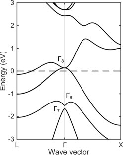
A further validation of our calculations is to show that the bandstructure of GaBi can be predicted accurately. The information on the band structure of GaBi is scarce. To date, calculations by Janotti et al. (2002) performed with LDA+ are considered state of the art. LDA+ is an empirical correction in the form of an additional atom-dependent radial potential, which is introduced in order to overcome shortcomings of LDA band structure Christensen (1984); Wei and Zunger (1998). The potential parameters for LDA+ are selected based on experimental band gaps and lattice constants of binary compounds, which is problematic in the case of GaBi. Therefore it will be useful to present results of all-electron DFT calculations for the band structure of GaBi obtained with TBmBJ correction.
To model the GaBi bandstructure, we used the GGA-WC exchange correlation functional as explained above. In the first step, the lattice constant of zinc-blend GaBi is optimized taking into account spin-orbit coupling. The result found here of Å is consistent with previous DFT calculations: 6.324, 6.28 and 6.47 Å Janotti et al. (2002); Ferhat and Zaoui (2006). This gives a lattice mismatch of 12% relative to GaAs (Tabs. 2 and 3), which hints that Bi atoms embedded in GaAs host lattices will give rise to large strains. This will be confirmed in the next section. Here, we used this to calculate the GaBi band structure shown in Fig. 1. Relativistic effects play an important role in the electronic structure of GaBi that is evident from a large spin-orbit splitting of eV. We find an inverted band structure with the state positioned energetically below the state, in agreement with Janotti et al. (2002). This arrangement results in a negative band gap of eV at point, which is comparable to the LDA+ calculations that yield the energy gap of eV Janotti et al. (2002). This additional test validates our WIEN2K calculations for Bi-containing compounds.
III Results and discussion
III.1 Comparison of strain and chemical effects in bandgap bowing
The 12% lattice mismatch between GaAs and GaBi binary compounds described above is consistent with the large difference between the covalent radii of As and Bi (1.19 vs. 1.48 Å, Cordero et al. (2008)). Using our computational methods we find that a Bi atom in GaAs host supercell gives a relaxed Ga-Bi bond longer by 7.5% than the Ga-As bond in pristine GaAs. This is the second largest magnitude of the local distortion field introduced in GaAs after nitrogen (Tab. 3). The valence band of GaAs is dominated by a deep As level and by three equal-energy As levels which give rise to the top of the valence band via overlaps between primitive cells A. X. Gray et al. (2011). This overlap and therefore the bandstructure can be perturbed by lattice strain as described by band deformation potentials Nolte et al. (1987). Including a Bi atom imposes such a strain in the host lattice, which is partially responsible for the bandgap variations in bismides. We call this the strain effect. An additional perturbation is due to the higher energy of the valence orbitals of Bi by comparison to the As orbitals, which we call the chemical effect.
| Compound111Results for N, P and Sb are adopted from Ref. 61. | 222The strain is calculated with respect to the equilibrium bond length in GaAs. |
|---|---|
| GaAs:N | |
| GaAs:P | |
| GaAs:Sb | |
| GaAs:Bi |
To delineate the strain and the chemical effects on the bowing in bismides we compare calculations that take into account the Bi chemistry with models where the Bi atoms are replaced back with As anions. We analyze two cases: first, periodic arrangements obtained with single Bi atoms in supercells of increasing sizes , and ; and second, a random distribution of Bi atoms in a supercell of size . In all cases, three electronic structures were obtained with the following models: (i.) frozen lattice, with atomic positions frozen to the host lattice, disregarding the local lattice distortions due to Bi; (ii.) relaxed lattice, with atomic positions relaxed by minimizing the forces arising to Bi incorporation, keeping the supercell size fixed; and (iii.) distorted pristine lattice, where the positions of atoms are taken from ii. and Bi is replaced back by As. The latter case allows to isolate changes in the host band structure caused solely by the lattice distortions Kent and Zunger (2001).
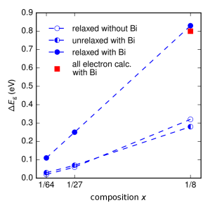
The calculations with a single Bi atom per supercell correspond to idealized crystals with unit cells of , , and atoms, respectively. The resulting bowing is given as a function of composition in Fig. 2. These were obtained with the PAW method (Sec. II.1), and we added a data point from an all-electron calculation (Sec. II.2) to show that the results are in good agreement. While at large concentrations the frozen lattice model shows a sizable bowing, but less than half of that from the relaxed lattice model, at low concentrations it shows a much smaller fraction. The distorted pristine lattice model gives bowing very similar to the frozen lattice model for all concentrations. The summation of the two is less than the bowing observed in the relaxed lattices, with a pronounced difference at small .
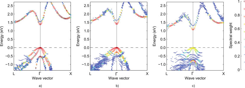
The results for a random distribution of Bi atoms in a supercell with atoms are shown in Fig. 3. These correspond to the composition of % Bi and were obtained with the all-electron method above (Sec. II.2). This large composition is relevant for telecom lasers with the emission wavelength of m and is close to the crossover between the band gap and spin-orbit splitting that takes place in GaAs1-xBix at % Usman et al. (2011, 2013). The alloy was represented by six As atoms randomly substituted by Bi. Three sets of calculations i-iii are performed according to the description above. The frozen lattice model applied to this alloy [Fig. 3 (a)] gives a mild perturbation of the pristine GaAs band structure induced by Bi disorder. The most noticeable changes occur in the valence band, such as an enhanced spin-orbit splitting and smeared Bloch character of states located well below the Fermi energy. The Bloch character of the conduction band remains almost unaffected. The distorted pristine lattice model [Fig. 3 (b)] shows a disorder in the conduction band from local lattice distortions but, more importantly, it shows that the valence band is perturbed to the extent that it looses its Bloch character for states with the energy eV, where it becomes hard to distinguish between heavy and light holes. Nevertheless, in this model the uppermost valence band preserves its Bloch character. The combined strain and chemical effects are seen in the relaxed lattice model [Fig. 3 (c)], which displays profound changes in the valence band: the Bloch character is deteriorated down to even for the edge of the valence band at the point. Such a low value is indicative of localization effects in the valence band, and it is correlated with an bowing larger than the sum of those in Figs. 3 (a,b). This corroboration of strain and chemical effects in decreasing is consistent with the previous observation from Fig. 2, and the change in for the alloy is quantitatively consistent with those from PAW method. We also observe in Fig. 3 (c) that the heavy hole band becomes progressively weaker (smaller spectral weight) and eventually disappears while moving deeper into the valence band. In spite of the disorder, the split-off band can be clearly identified. The conduction band is overall less disturbed and retains 80% of its character.
The trends noticed here for a random distribution of Bi atoms are consistent with the results obtained using a tight binding model Usman et al. (2013, 2011). In addition, the observations made for both the random and the regular distributions point towards a hybridization of Bi orbitals mainly with the heavy and light hole bands throughout a large energy interval including the valence band edge, and also to interactions between Bi atoms. In the next paragraph we provide an understanding of both effects by looking at clusters of Bi atoms.
III.2 Bi complexes
The random distribution in Fig. 3 for six Bi atoms among the sites of a supercell corresponds to a concentration of , between the ordered-Bi arrangements with and in Fig. 2. The latter two imply Bi-Bi distances of three, respectively two lattice spacings in all directions, whereas random distributions like that in Fig. 3 can include nearest neighbors, next-nearest neighbors, etc. A given concentration can be modeled with more than one Bi atom per supercell, e.g., can be modeled as above with one Bi atom per supercell, or with eight Bi atoms in a supercell, etc., which is expected to produce a distribution of data points in Fig. 2. This is exactly what we find in Fig. 4 below, obtained with the approach described in the next paragraph. The following models have been analyzed in order to understand some aspects of Bi-atom clustering and to make initial steps towards interpreting experiments, in particular for high concentrations . We address the bowing for combinations of two, three, and four Bi atoms, respectively, and then we analyze the electronic bandstructure of two Bi atoms in several relative positions. For these calculations we used the PAW method (Sec. II.1) and included the atomic relaxation inside the supercell.
We considered several different Bi complexes in a -atom supercell and observed the bowing. We took the first Bi atom to be at the origin and specified the other Bi atoms by their positions relative to it through =. Here, , are are the two-atom primitive lattice vectors. First, we constructed three arrangements for each concentration , , , shown in Tab. 4: chains along axis , chains along axis and clusters (in which all Bi are closest to origin along and directions). In addition, for this -atom supercell we used the ATAT package van de Walle et al. (2002); van de Walle (2009) to obtain special quasirandom structures (SQS) Zunger et al. (1990); van de Walle et al. (2013). These structures are as close energetically as possible with periodic supercells to the true disordered state. We chose the pair length to include third nearest neighbours, the triplet length to include second nearest neighbours and the quadruplet length to include nearest neighbours. The difference from the correlation functions of the supercells we obtained to the correlation functions of the true disordered state are all smaller than .
| Arrangement | 2 atoms | 3 atoms | 4 atoms | [meV/Bi] | |
| chain | {(0,0,0), | {(0,0,0), | {(0,0,0), | ||
| (2,0,0)} | (1,0,0), | (1,0,0), | |||
| (2,0,0)} | (2,0,0), | ||||
| (3,0,0)} | |||||
| 1.15 | 0.87 | 0.52 | |||
| 0.39 | 0.27 | 0.67 | |||
| chain | {(0,0,0), | {(0,0,0), | {(0,0,0), | ||
| (2,2,2)} | (2,2,2), | (1,1,1), | |||
| (3,3,3)} | (2,2,2), | ||||
| (3,3,3)} | |||||
| 1.28 | 1.23 | 1.19 | |||
| 0.31 | 0.18 | 0.33 | |||
| clustered | {(0,0,0), | {(0,0,0), | {(0,0,0), | ||
| (1,0,0)} | (1,0,0), | (1,0,0), | |||
| (pair) | (0,1,0)} | (0,1,0), | |||
| (trimer) | (0,0,1)} | ||||
| (tetramer) | |||||
| 1.12 | 0.96 | 0.90 | |||
| 0.36 | 0.25 | 0.73 | |||
| SQS | |||||
| 1.32 | 1.19 | 1.18 | |||
| 0.00 | 0.00 | 0.00 |
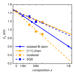
Tab. 4 shows the obtained band gaps for all arrangements considered, along with the total energy difference between each arrangement and the SQS structure at a given concentration. In all cases, the SQS are energetically most stable. The other arrangements for a given differ only slightly in their total energy (less than eV), with the chain preferred after the SQS. The exception is the chain arrangement of four atoms, which is considerably more stable than the chain and tetramer for this concentration. The last column in the table shows the slope of the band gap bowing for each of these arrangement types, obtained from the linear interpolation shown in Fig. 4. These are compared with the bowing from ordered Bi atoms shown in Fig. 2, which gave a slope of meV/Bi.
Tab. 4 and Fig. 2 show that the bowing closest to the meV/%Bi range of experimental values found in the literature Tixier et al. (2003); Huang et al. (2005); Francoeur et al. (2003) correspond to the isolated Bi atom and cluster arrangements. Nevertheless, these are not the most favorable total energy states, which may be due to fixing the size of the supercell. These are followed by the bandgap bowing of the chains and of the SQS structures, close to one another but somewhat smaller than the experimental values cited. It is worth noticing that these are our lowest total energy arrangements, and the difference in bowing from the experimental values may be partially due to constraining the size of the supercells. Finally, the bowing for the chains is considerably larger than both the experimental values and the other theoretical values obtained here.
The spread in the slopes described here suggests that differences in growth techniques or growth parameters can lead to differences in the observed band gap reduction as a function of Bi concentration, which can be caused by the differences in the Bi atom arrangements in the samples. Consequently, measuring the band gap reduction with increasing Bi concentration can potentially help in identifying the types of Bi arrangement distributions in the samples. For example, for growing conditions that fix the lattice constant to that of a GaAs substrate, our results point towards regular Bi distributions or cluster arrangements as the most likely candidates.
For random Bi distributions at high concentrations like that in Fig. 3, the resulting band structure can be understood intuitively as an ’average’ of band structures of complexes like those discussed here. Different local configurations would contribute to the effective band structures with weights determined by their total energies. A detailed statistics is beyond the scope of this paper, but the large distributions of is identified clearly as a factor in the degradation of the Bloch character of the valence band edge seen in Fig. 3.
III.3 Electronic structure of Bi pairs
To obtain an insight into the unfolded band structures from Fig. 3 and into the distribution of bowing seen in Tab. 4 and Fig. 4, we look at the detailed band structure of complexes of two Bi atoms aligned along the axis or along the axis. The former case is relevant for the extraordinary large bowing seen in the previous section for the chains. The latter is relevant for the energy-favorable case of chains, which gives the lowest bowing, albeit one closer to the experimental range. All the calculations from this section are performed with PAW-PP in VASP.
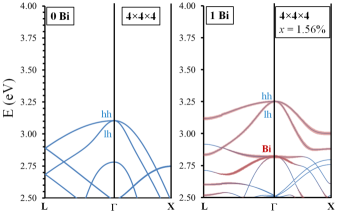
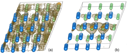
First, we obtain the single Bi band structure shown in Fig. 5 for a -atom cell side by side with the folded pristine GaAs band structure. It is seen that the defect level hybridizes strongly with the heavy hole (hh) and light hole (lh) bands and contributes significantly to the valence band edge and to the flat defect level next to the split-off band. There is virtually no hybridization with the split-off band. The splitting of the hh and lh bands gives rise to localized states at the edge of the Brillouin zone, which will contribute to the loss of Bloch character in disordered structures like that in Fig. 3. Fig. 6(a,b) shows a comparison between the -point wavefunctions of pristine GaAs and of a single Bi atom, for the hh state and the defect state. It proves the hybridization of Bi orbitals with the nearest neighbor As orbitals and the localization of the state.
(a)
(b)
(c)
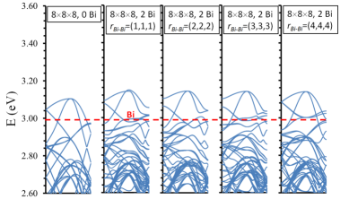
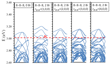
Next, we consider the band structure of two Bi atoms in a -atom cell (Fig. 7). There is a clear difference between the alignment along the and the directions: the valence band edge is raised considerably more in the former case. This is due to different distances between the two Bi atoms: along and along . The defect levels move away from the so-band, and there is a spin-orbit splitting of hh, lh, and defect bands in the cases due to lower symmetry. Fig. 6(c) shows the -point wavefunctions for the pair, proving the strong overlap between the orbitals of the two Bi atoms.
All configurations shown in (Fig. 7) correspond to the same concentration but give a wide range of bowing values, which shows that the overlaps between orbitals of Bi is strongly anisotropic. The strong interaction between two neighboring Bi atoms can perturb significantly the valence band even for smaller concentrations, depending on their relative position, as seen in Figs. 8 and 9 for () calculations with VASP. This size of supercell minimizes the interaction between image Bi atoms. Again, it is seen that a large perturbation occurs in the configuration of the pair. This set of calculations proves that at small concentrations the clustering is minimal, otherwise it would be observed as a larger bowing than that seen in experiments.

The localization and hybridization effects observed in 6(b,c) are consistent with the real-space interpretation of dilute nitride and bismide band structures Kent and Zunger (2001); Virkkala et al. (2013b, a). In that interpretation, the main argument is the accumulation of electron charge at single impurity centers. The charge was integrated over the entire defect band. Here we provided a more detailed picture in terms of hybridization and localization of specific wavefunctions for interacting defects. Our argumentation can be complemented with a real-space description of charge accumulation at Bi complexes, which is relevant for the formation of covalent bonds between impurities. This is shown in Fig. 10 for the example of the heavy hole band for the two atom chain and pair arrangements from Tab. 4. The charge accumulation can be observed in the case of the cluster [Fig. 10(b)] while such an accumulation is absent when the Bi atoms are dispersed [Fig. 10(a)].
IV Conclusions
In this work we performed a detailed analysis of three factors influencing the bandgap bowing in dilute alloys: the chemical effect, the strain effect, and the effect of disorder. We found that the strain induced in the lattice by the Bi atoms is responsible for a good part of the bandgap bowing, in particular for large concentrations . To understand the effective band structures at high concentrations, we analyzed the contribution of various cluster configurations to the band bowing. We found that the latter depends strongly on the structure of clusters considered. We provided an understanding of the range of bowing rates observed based on the anisotropic, strongly coordinate-dependent interaction between Bi atoms. We suggest that the two-scale disorder observed in PL experiments at high Bi concentration can be understood intuitively as coming from an average of valence band perturbations like those seen here, or from an effective band structure with a significant degradation of the Bloch character throughout the Brillouin zone. The results from the models analyzed here suggest that some band bowing measurements performed on samples grown in different conditions can be interpreted in terms of special Bi configurations like those studied here.
Acknowledgements.
The Marburg part of the work was funded by the DFG via the GRK 1782 ”Functionalization of Semiconductors”; computing time from HRZ Marburg, CSC Frankfurt, and HLRS Stuttgart is acknowledged. OR would like to acknowledge funding provided by the Natural Sciences and Engineering Research Council of Canada under the Discovery Grant Program RGPIN-2015-04518. The work in USA was supported by the AFOSR, the NLCSTR contributions via a phase-II STTR.References
- Oe and Okamoto (1998) K. Oe and H. Okamoto, Jpn. J. Appl. Phys. 37, L1283 (1998).
- Francoeur et al. (2003) S. Francoeur, M.-J. Seong, A. Mascarenhas, S. Tixier, M. Adamcyk, and T. Tiedje, Appl. Phys. Lett. 82, 3874 (2003).
- Broderick et al. (2012) C. A. Broderick, M. Usman, S. J. Sweeny, and E. P. O’Reilly, Semicond. Sci. Technol. 27, 094011 (2012).
- Usman et al. (2013) M. Usman, C. A. Broderick, Z. Batool, K. Hild, T. J. C. Hosea, S. J. Sweeny, and E. P. O’Reilly, Phys. Rev. B 87, 115104 (2013).
- Sweeny et al. (2011) S. J. Sweeny, Z. Batool, K. Hild, S. R. Jin, and T. J. C. Hosea, in International Conference on Transparent Optical Networks (2011) pp. 1–4.
- Sweeny and Jin (2013) S. J. Sweeny and S. R. Jin, J. Appl. Phys. 113, 043110 (2013).
- Batool et al. (2013) Z. Batool, S. Chatterjee, A. Chernikov, A. Duzik, R. Fritz, C. Gogieni, K. Hild, T. J. C. Hosea, S. Imhof, and S. R. Johnson, “Molecular beam epitaxy: From research to mass production,” (Elsevier Inc., 2013) Chap. Bismuth-containing III-V semiconductors: Epitaxial growth and physical properties, pp. 139–158.
- Ludewig et al. (2013a) P. Ludewig, N. Knaub, W. Stolz, and K. Volz, J. Cryst. Growth 370, 186 (2013a).
- Ludewig et al. (2013b) P. Ludewig, N. Knaub, N. Hossain, S. Reinhard, L. Nattermann, I. P. Marko, S. R. Jin, K. Hild, S. Chatterjee, and W. Stolz, Appl. Phys. Lett. 102, 242115 (2013b).
- Butkute et al. (2014) R. Butkute, A. Geizutis, V. Pacebutas, B. Cechavicius, V. Bukauskas, R. Kundrotas, P. Ludewig, K. Volz, and A. Krotkus, Electronic Letters 50, 1155 (2014).
- Grüning et al. (2004) H. Grüning, K. Kohary, S. D. Baranovskii, O. Rubel, P. J. Klar, A. Ramakrishnan, G. Ebbinghaus, P. Thomas, W. Heimbrodt, and W. Stolz, Phys. Status Solidi B 1, 109 (2004).
- Rubel et al. (2005) O. Rubel, M. Gallupi, S. D. Baranovskii, K. Volz, L. Geelhaar, H. Riechert, P. Thomas, and W. Stolz, J. Appl. Phys. 98, 063518 (2005).
- Jandieri et al. (2012) K. Jandieri, M. K. Shakfa, S. Liebich, M. Zimprich, B. Kunert, C. Karcher, A. Chernikov, K. Volz, W. Stolz, and M. Koch, Phys. Rev. B 86, 125318 (2012).
- Karcher et al. (2013) C. Karcher, K. Jandieri, B. Kunert, R. Fritz, K. Volz, W. Stolz, F. Gebhard, S. D. Baranovskii, and W. Heimbrodt, J. Lumin. 133, 125 (2013).
- Virkkala et al. (2012) V. Virkkala, V. Havu, F. Tuomisto, and M. J. Puska, Phys. Rev. B 85, 085134 (2012).
- Virkkala et al. (2013a) V. Virkkala, V. Havu, F. Tuomisto, and M. J. Puska, Phys. Rev. B 88, 035204 (2013a).
- Kini et al. (2011) R. N. Kini, A. J. Ptak, B. Fluegel, R. France, R. C. Reedy, and A. Mascarenhas, Phys. Rev. B 83, 075307 (2011).
- Nargelas et al. (2011) S. Nargelas, K. Jarasiunas, K. Bertulis, and V. Pacebutas, Appl. Phys. Lett. 98, 082115 (2011).
- Beaton et al. (2010) D. A. Beaton, R. B. Lewis, M. Masnadi-Shirazi, and T. Tiedje, J. Appl. Phys. 108, 083708 (2010).
- Cooke et al. (2006) D. G. Cooke, F. A. Hegmann, E. C. Young, and T. Tiedje, Appl. Phys. Lett. 89, 122103 (2006).
- Usman et al. (2011) M. Usman, C. A. Broderick, A. Lindsay, and E. P. O’Reilly, Phys. Rev. B 84, 245202 (2011).
- Deng et al. (2010) H. X. Deng, J. Li, S. S. Li, H. Peng, J. B. Xia, L. W. Wang, and S. H. Wei, Phys. Rev. B 82, 193204 (2010).
- Virkkala et al. (2013b) V. Virkkala, V. Havu, F. Tuomisto, and M. J. Puska, Phys. Rev. B 88, 235201 (2013b).
- Rubel et al. (2014) O. Rubel, A. Bokhanchuk, S. J. Ahmed, and E. Assmann, Phys. Rev. B 90, 115202 (2014).
- Imhof et al. (2010a) S. Imhof, A. Thränhardt, A. Chernikov, M. Koch, N. S. Köster, S. Chatterjee, S. W. Koch, X. Lu, S. R. Johnson, and D. A. Beaton, Appl. Phys. Lett. 96, 131115 (2010a).
- Imhof et al. (2010b) S. Imhof, C. Wagner, A. Chernikov, M. Koch, K. Kolata, N. S. Köster, S. Chatterjee, S. W. Koch, and X. F. Lu, Phys. Status Solidi B 248, 851 (2010b).
- Imhof et al. (2011) S. Imhof, C. Wagner, A. Thränhardt, A. Chernikov, M. Koch, N. S. Köster, S. Chatterjee, S. W. Koch, and O. Rubel, Appl. Phys. Lett. 98, 161104 (2011).
- Shakfa et al. (2013) M. K. Shakfa, D. Kalincev, X. Lu, S. R. Johnson, D. A. Beaton, T. Tiedje, A. Chernikov, S. Chatterjee, and M. Koch, J. Appl. Phys. 114, 164306 (2013).
- Shakfa et al. (2015) M. K. Shakfa, M. Wiemer, L. P., K. Jandieri, K. Volz, W. Stolz, S. D. Baranovskii, and M. Koch, J. Appl. Phys. 117, 025709 (2015).
- Puustinen et al. (2013) J. Puustinen, M. Wu, E. Luna, A. Schramm, P. Laukkanen, M. Laitinen, T. Sajavaara, and M. Guina, J. Appl. Phys. 114, 243504 (2013).
- Ciatto et al. (2008) G. Ciatto, E. C. Young, F. Glas, J. Chen, R. Alonso Mori, and T. Tiedje, Phys. Rev. B 78, 035325 (2008).
- Kim et al. (2009) Y.-S. Kim, K. Hummer, and G. Kresse, Phys. Rev. B 80, 035203 (2009).
- Kim et al. (2010) Y.-S. Kim, M. Marsman, G. Kresse, F. Tran, and P. Blaha, Phys. Rev. B 82, 205212 (2010).
- Blöchl (1994) P. E. Blöchl, Phys. Rev. B 50, 17953 (1994).
- Kresse and Joubert (1999) G. Kresse and D. Joubert, Phys. Rev. B 59, 1758 (1999).
- Kresse and Hafner (1993) G. Kresse and J. Hafner, Phys. Rev. B 47, 558 (1993).
- Kresse and Hafner (1994) G. Kresse and J. Hafner, Phys. Rev. B 49, 14251 (1994).
- Kresse and Furthmüller (1996a) G. Kresse and J. Furthmüller, Comp. Mater. Sci. 6, 15 (1996a).
- Kresse and Furthmüller (1996b) G. Kresse and J. Furthmüller, Phys. Rev. B 54, 11169 (1996b).
- Blaha et al. (2001) P. Blaha, K. Schwarz, G. K. H. Madsen, D. Kvasnicka, and J. Luitz, “WIEN2k: An Augmented Plane Wave + Local Orbitals Program for Calculating Crystal Properties,” (2001).
- Perdew and Wang (1992) J. P. Perdew and Y. Wang, Phys. Rev. B 45, 13244 (1992).
- Perdew et al. (1996) J. P. Perdew, K. Burke, and M. Ernzerhof, Phys. Rev. Lett. 77, 3865 (1996).
- Perdew et al. (1997) J. P. Perdew, K. Burke, and M. Ernzerhof, Phys. Rev. Lett. 78, 1396 (1997).
- Perdew et al. (2008) J. P. Perdew, A. Ruzsinsky, G. I. Csonka, O. A. Vydrov, G. E. Scuseria, L. A. Constantin, X. Zhou, and K. Burke, Phys. Rev. Lett. 100, 136406 (2008).
- Grimme et al. (2010) S. Grimme, J. Antony, S. Ehrlich, and H. Krieg, J. Chem. Phys. 132, 054104 (2010).
- Grimme et al. (2011) S. Grimme, S. Ehrlich, and L. Goerigk, J. Comp. Chem. 32, 1456 (2011).
- Monkhorst and Pack (1976) H. J. Monkhorst and J. D. Pack, Phys. Rev. B 13, 5188 (1976).
- Tran and Blaha (2009) F. Tran and P. Blaha, Phys. Rev. Lett. 102, 226401 (2009).
- Mad (2004) Semiconductors: Data Handbook (Springer-Verlag Berlin Heidelberg, 2004).
- Blakemore (1982) J. S. Blakemore, J. Appl. Phys. 53, R123 (1982).
- Lautenschlager et al. (1987) P. Lautenschlager, M. Garriga, S. Logothetidis, and M. Cardona, Phys. Rev. B 35, 9174 (1987).
- Wu and Cohen (2006) Z. Wu and R. E. Cohen, Phys. Rev. B 73, 235116 (2006).
- Haas et al. (2009) P. Haas, F. Tran, and P. Blaha, Phys. Rev. B 79, 085104 (2009).
- Janotti et al. (2002) A. Janotti, S. H. Wei, and S. B. Zhang, Phys. Rev. B 65, 115203 (2002).
- Christensen (1984) N. E. Christensen, Phys. Rev. B 30, 5753 (1984).
- Wei and Zunger (1998) S. H. Wei and A. Zunger, Phys. Rev. B 57, 8983 (1998).
- Ferhat and Zaoui (2006) M. Ferhat and A. Zaoui, Phys. Rev. B 73, 115107 (2006).
- Cordero et al. (2008) B. Cordero, Gómez, A. E. Platero-Prats, M. Revés, J. Echeverría, E. Cremades, F. Barragán, and S. Alvarez, Dalton Trans. , 2832 (2008).
- A. X. Gray et al. (2011) A. X. Gray et al., Nature Materials 10, 759–764 (2011).
- Nolte et al. (1987) D. D. Nolte, W. Walukiewicz, and E. E. Haller, Phys. Rev. Lett. 59, 501 (1987).
- Rubel et al. (2008) O. Rubel, I. Németh, W. Stolz, and K. Volz, Phys. Rev. B 78, 075207 (2008).
- Kent and Zunger (2001) P. R. C. Kent and A. Zunger, Phys. Rev. B 64, 115208 (2001).
- van de Walle et al. (2002) A. van de Walle, M. Asta, and G. Ceder, Calphad 26, 539 (2002).
- van de Walle (2009) A. van de Walle, Calphad 33, 266 (2009).
- Zunger et al. (1990) A. Zunger, S. H. Wei, L. G. Ferreira, and J. E. Bernard, Phys. Rev. Lett. 65, 353 (1990).
- van de Walle et al. (2013) A. van de Walle, P. Tiwary, M. M. de Jong, D. L. Olmsted, M. D. Asta, A. Dick, D. Shin, Y. Wang, L. Q. Chen, and Z. K. Liu, Calphad 42, 13 (2013).
- Tixier et al. (2003) S. Tixier, M. Adamcyk, T. Tiedje, S. Francoeur, A. Mascarenhas, P. Wei, and F. Schiettekatte, Appl. Phys. Lett. 82, 2245 (2003).
- Huang et al. (2005) W. Huang, K. Oe, G. Feng, and M. Yoshimoto, J. Appl. Phys. 98, 053505 (2005).