Spin-orbit coupling measurement by the scanning gate microscopy
Abstract
We propose a procedure for extraction of the Fermi surface for a two-dimensional electron gas with a strong Rashba spin-orbit coupling from conductance microscopy. Due to the interplay between the effective spin-orbit magnetic field and the external one within the plane of confinement, the backscattering induced by a charged tip of an atomic force microscope located above the sample, leads to the spin precession, and thus to the spin mixing of the incident and reflected modes.This mixing leads to a characteristic angle-dependent beating pattern visible in the conductance maps. We show that the structure of the Fermi level, bearing signatures of the spin-orbit coupling, can be extracted from the Fourier transform of the interference fringes in the conductance maps as a function of the magnetic field direction. We propose a simple analytical model which can be used to fit the experimental data in order to obtain the spin-orbit coupling constant.
Introduction. Charge carriers in semiconductors are subject to spin-orbit (SO) interactions Manchon2015 due to electric fields or anisotropy of the crystal lattice. The consequences of these interactions, including spin relaxation and dephasing Ohno1999 ; Dyakonov1971 ; Kainz2004 , spin Hall effects Hirsch1999 ; Sinova2004 ; Kato2004 , topological insulators Koenig2007 , persistent spin helix states Bernevig2006 ; Koralek2009 ; Walser2012 , Mayorana fermions Mourik2012 etc., are extensively studied e.g.. A spin-active devices, including spin-filters based on quantum point contacts (QPCs) Debray2009 , spin transistors Datta1990 ; Schliemann2003 ; Zutic2004 ; Chuang2015 ; Bednarek2008 , exploiting the precession of the electron spin in the SO effective magnetic field Meier , are well known examples. The most popular playground for spin effects and spin-active devices is the two-dimensional electron gas (2DEG) in III-V heterostructures, which show a strong built-in electric fields in the confinement layer, giving rise to the Rashba SO coupling Bychkov1984 . The knowledge of the SO interaction strength is of fundamental importance for description of spin devices and phenomena. The measurements of the SO coupling constant are usually analyzed from the Shubnikov-de Haas Nitta1997 ; Engels1997 ; Lo2002 ; Kwon2007 ; Grundler2000 ; Kim2010 ; Das1989 ; Park2013 oscillations, antilocalization as observed in the magnetotransport Koga2002 , photocurrents Ganichev2004 , or precession of optically polarized electron spins as a function of their drift momentum Meier2007 .
The SO coupling produces a shift of the spin-up and spin-down dispersion relations on the wave vector scale Manchon2015 that is a linear function of the SO coupling constant. In this Letter we propose a way to extract the structure of the dispersion relation near the Fermi level Manchon2015 using spin-dependent scattering and the resulting interference with the scanning gate microscopy Sellier2011 ; Ferry2011 (SGM) applied to systems with QPCs Topinka2001 ; Schnez2011 . In this technique, the tip acts as a floating perturbation of the potential landscape as seen by the Fermi level electrons. As a result the recorded SGM images contain interference fringes due to the incident and backscattered electron waves Jura2007 ; Jura2009 . In presence of an in-plane magnetic field the fringes form beating pattern due to spin-dependence of the Fermi wavelengths Kleshchonok2015 . In this Letter we analyze the beating patterns that appear for SO-coupled systems. The electron – when scattered – experiences precession of its spin due to rotation of the momentum-dependent effective magnetic field Meier2007 , and the interference of the incident and reflected electron waves potentially involves spin-mixing effects. However, we find that in the absence of the external magnetic field the backscattering involves a pure inversion of the effective field with no precession effect. The latter are triggered by an external in-plane magnetic field, and lead to an appearance of the dependence of the beating patterns on the orientation of the magnetic field. We demonstrate that the shape of the Fermi level structure and thus the SO coupling constant can be traced back from the beating patterns by Fourier transform analysis.
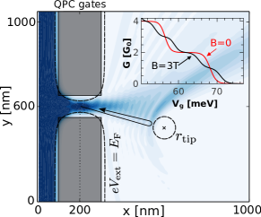
Theory. We consider Fermi level transport in a 2DEG with a local constriction QPC as depicted in Fig. 1. The Fermi level electrons travel from the electron reservoir placed at nm through a channel modeled with an infinite potential step and an additional potential tuned by gates (gray areas of the scheme). A negatively charged tip acts as a backscatterer to the right of the QPC. The conductance maps as functions of the tip position resolve the coherent interference fringes as observed in a number of experiments Topinka2000 ; Topinka2001 ; Jura2007 ; Jura2009 ; Kozikov2015 . The part of the system to the right of the QPC is considered open such that electron may freely propagate without reflections. Transparent boundary conditions for the electron flow are introduced with a method described in Ref. Nowak2014 .
We adopt a standard two-dimensional model assuming that all the electrons of 2DEG occupy a strongly localized lowest-energy state of the vertical quantization. The Hamiltonian accounts for the Rashba SO interaction and a presence of the external magnetic field applied within the plane of confinement
| (1) |
with , , and is the vector of Pauli matrices. The external potential is a superposition of two components: (i) – the QPC gate potential modeled with analytical formulas for a rectangle gate adapted from Ref. Davies1995 , and (ii) – the electrostatic potential created by the charged tip of the scanning probe. The tip potential is modeled by the Lorentzian profile given by with effective width nm, which is of order of the distance between 2DEG and surface of the sample, and that depends on the voltage applied to the tip. This form of the potential results from the screening of the tip charge by 2DEG kolasinskiDFT2013 ; Steinacher2015 . The Rashba Hamiltonian in Eq. (1) comes from the electrostatic confinement of the 2DEG in the growth direction Bhandari2013 . We apply the symmetric gauge . By choosing the plane of the 2DEG confinement to be located at , we get , and the magnetic field enters the Hamiltonian only via the spin Zeeman term.
The scattering problem is solved within the finite difference approach Kolasinski2016Lande with spatial discretization nm using the wave function matching (WFM) method Zwierzycki2008 . Then we calculate conductance using the Landauer approach by evaluating at the Fermi level (with ). For simplicity, we consider the case of single mode transmitting through the QPC () (see the inset to Fig. 1). We set meV (for the Fermi wavelength is nm), and the tip potential meV for which a strict depletion of the electron density below the tip is obtained (see dashed circle in Fig. 1). Landé factor is assumed to be and effective mass as for InGaAs.
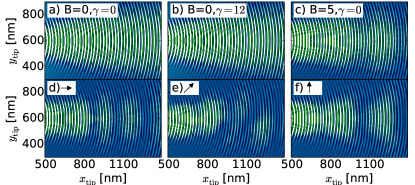
Results and Discussion. Figs. 2(a-f) show spatial derivatives of SGM images obtained from the solution of the quantum scattering problem for QPC in Fig. 1 tuned to the first QPC conductance plateau. For and [Fig. 2(a)] a pronounced interference pattern of the incident and backscattered wave is observed Topinka2001 ; Schnez2011 ; Jura2007 ; Jura2009 with the period of for both [Fig. 2(a)] and [Fig. 2(b)]. A beating pattern Kleshchonok2015 appears at non-zero [Fig. 2(c)], which depends on the orientation of the in-plane field for (Figs. 2 (d-f)).
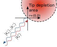
In order to explain the results of Fig. 2 we consider a simple model for SGM images in presence of in-plane magnetic field and SO interaction. The electron wave which leaves the QPC Kolasinski2014Slit ; Kolasinski2015 ; Jalabert2010 ; Khatua2014 is approximated by a plain wave (an inverse of the square root of the distance from the QPC is neglected as slowly varying). The schematics of the considered scattering process is presented in Fig. 3. The electron wave which leaves the QPC (not shown in the diagram) propagates through the device until it is backscattered by the potential barrier created by the SGM tip with probability 1. We fix the origin at the scattering point. For a given incoming spin state the scattering wave function can be expanded in terms of the possible scattering modes
| (2) |
where and denotes the absolute value of the wave vector of an electron in spin state . The sign in the superscript indicates the electron incoming from left or backscattered by the tip . The values of the scattering amplitudes depend on a specific situation.For SO coupling and magnetic field simultaneously present, the Hamiltonian for a free electron can be written
| (3) |
where and . Plain wave solution for the Schrödinger equation gives two eigenvalues
| (4) |
where , with and
| (5) |
where denotes the value of vector, are eigenvectors for incoming and outgoing directions of an electron. Due to the assumed infinite potential generated by the SGM tip, the scattering wave function in Eq. (2) has to vanish at (see Fig. 3)
By substituting Eq. (5) to this equation one evaluates the scattering amplitudes .
For the simplest case when SOI and magnetic field are not present in the Hamiltonian (3) the propagating modes in Eq. (5) reduce to
with and scattering amplitudes , from which one finds that reflection does not change the spin orientation. The scattering wave function from Eq. (2) is then
and the scattering density is given by and the variation of the map follows the pattern of the density Kolasinski2014Slit , The SGM conductance pattern can be approximated by . The SGM image obtained with this model is presented in Fig. 4(a) and is consistent with the simulated image obtained in Fig. 2.
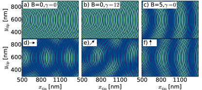
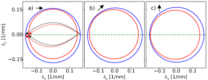
For and one may easily check that the propagating modes [Eq. (5)] still satisfy orthogonality relations and , which leads to the spin conserving reflection . However in this case and the scattering wave function is given by . The electron density is then proportional to . However, using the fact that Bercioux2015 we get the same expression as for i.e. , which does not depend on electron spin. Hence the SO effect vanishes for the backscattering process which leads to the same SGM image [Fig. 4(b)] as in case of [Fig. 4(a)].
The third possible configuration of parameters i.e. and was recently discussed in Ref. Kleshchonok2015 . In this case the same orthogonality relation is still satisfied , and . However, the resulting electron density is now proportional to and depends on the spin via the Zeeman term in Eq. (4) inducing shifts of . The approximated SGM map gives a signal being a superposition of two frequencies resulting in the beating pattern visible in Fig. 4(c). The present reasoning explains the findings of Ref. Kleshchonok2015 .
In a general case of and the eigenvalues (4) depend on both the direction of magnetic field and the propagation vector, thus the spin will not be conserved anymore during the backscattering process, since the orthogonality relations between the incident and backscattered modes no longer hold , and .The resulting electron density will be then a composition of four different possible superposition of the Fermi wave vectors . The SGM images obtained for this general case for three different orientation of magnetic field are depicted in Figs. 4(d-f). Although, the images differ somewhat from Fig. 4 (d-f), still both the model and the full simulation allow for extraction of the wave vectors and their dependence on the orientation of the magnetic field in the Fourier analysis (see below).
The form of Eq. (3) indicates that rotation of a SGM tip position along the arc centered at the QPC entrance is equivalent to a rotation of the in-plane magnetic field (in an opposite direction) for a fixed tip position. For a practical implementation of an experiment it should be more efficient to perform a SGM scan along a straight line, where the longest electron branch Topinka2000 ; Kozikov2015 is present and rotate the magnetic field instead (see Fig. 5(a)).
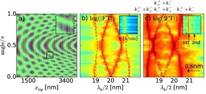
In Fig. 5(b-c) we present the Fourier transform (FT) of the conductance signal calculated from the map for the tip moving along the QPC axis, as a function of the magnetic field direction B for T. The results are plotted on the wavelength scale calculated as . The dashed lines in Figs. 5(b-c) were plotted for backscattering processes that are explained in Fig. 6(a) and calculated numerically from the condition with the latter given by Eq. (4). Note, that due to the smooth and extended shape of the the tip potential in the full simulation the resonance lines in Fig. 5(c) are slightly shifted to the left by 0.8nm (in comparison to model Fig. 5(b)). We accordingly shifted the dashed lines in Fig. 5(c) to coincide with the FT image. In the inset in Fig. 5(c) one observes also higher harmonics, which result from the possible multiple reflections between the tip and QPC (not present in the model, see inset in Fig. 5(b)).
The backscattering taken along the axis of the QPC involves and we find in general four various values of visible as four lines in FT images. However, when , Eq. (4) reduces to
| (6) |
which is symmetric with respect to electron reflection , which implies the symmetry o scattering process that (see Fig. 6(a)), and thus reducing the number of resonance lines in FT image to two. For other cases presented in Figs. 6(b-c) this symmetry is not satisfied and all four frequencies are visible.
Summary. In summary, we have shown that SGM imaging can be used to extract the Fermi surface properties by Fourier analysis of the beatings due to the SO interaction and an in-plane magnetic field. The analysis allows for deduction of the Rashba constant from the real space measurement of conductance as a function of the tip position involving spin-scattering in a crossed external and built-in magnetic fields.
Acknowledgments This work was supported by National Science Centre according to decision DEC-2015/17/N/ST3/02266, and by PL-Grid Infrastructure. The first author is supported by the scholarship of Krakow Smoluchowski Scientific Consortium from the funding for National Leading Reserch Centre by Ministry of Science and Higher Education (Poland) and by the Etiuda stipend of the National Science Centre (NCN) according to decision DEC-2015/16/T/ST3/00310.
References
- (1) A. Manchon, H. C. Koo, J. Nitta, S. M. Frolov, and D. R. A., Nat. Mater. 14, 871 (2015)
- (2) Y. Ohno, R. Terauchi, T. Adachi, F. Matsukura, and H. Ohno, Phys. Rev. Lett. 83, 4196 (1999)
- (3) M. I. D’yakonov and V. I. Perel, JETP Lett. 13, 467 (1971)
- (4) J. Kainz, U. Rössler, and R. Winkler, Phys. Rev. B 70, 195322 (2004)
- (5) J. E. Hirsch, Phys. Rev. Lett. 83, 1834 (1999)
- (6) J. Sinova, D. Culcer, Q. Niu, N. A. Sinitsyn, T. Jungwirth, and A. H. MacDonald, Phys. Rev. Lett. 92, 126603 (2004)
- (7) Y. K. Kato, R. C. Myers, A. C. Gossard, and D. Awschalom, Science 1910, 306 (2004)
- (8) M. Koenig, S. Wiedmann, C. Bruene, A. Roth, H. Buhmann, L. W. Molenkamp, X.-L. Qi, and Z. S.-C., Science 318, 766 (2007)
- (9) B. A. Bernevig, J. Orenstein, and S.-C. Zhang, Phys. Rev. Lett. 97, 236601 (2006)
- (10) J. D. Koralek, C. P. Weber, J. Orenstein, B. A. Bernevig, S.-C. Zhang, S. Mack, and D. D. Awschalom, Nature 458, 610 (2009)
- (11) M. P. Walser, C. Reichl, W. Wegscheider, and G. Salis, Nature Phys. 8, 757 (2012)
- (12) V. Mourik, K. Zuo, S. M. Frolov, S. R. Plissard, E. P. A. M. Bakkers, and L. P. Kouwenhoven, Science 336, 1003 (2012)
- (13) P. Debray, S. M. S. Rahman, J. Wan, R. S. Newrock, M. Cahay, A. T. Ngo, S. E. Ulloa, S. T. Herbert, M. Muhammad, and J. M., Nature Nanotech. 4, 759 (2009)
- (14) S. Datta and B. Das, Appl. Phys. Lett. 56, 665 (1990)
- (15) J. Schliemann, J. C. Egues, and D. Loss, Phys. Rev. Lett. 90, 146801 (2003)
- (16) I. Žutić, J. Fabian, and S. Das Sarma, Rev. Mod. Phys. 76, 323 (2004)
- (17) P. Chuang, S.-C. Ho, L. W. Smith, F. Sfigakis, M. Pepper, C.-H. Chen, J.-C. Fan, J. P. Griffiths, I. Farrer, H. E. Beere, G. A. C. Jones, D. A. Ritchie, and T.-M. Chen, Nat Nano 10, 35 (2015)
- (18) S. Bednarek and B. Szafran, Phys. Rev. Lett. 101, 216805 (2008)
- (19) L. Meier, G. Salis, I. Shorubalko, E. Gini, S. Schoen, and K. Ensslin, Nature Phys. 3 (2007)
- (20) Y. Bychkov and E. Rashba, J. Phys. C 17, 6039 (1984)
- (21) J. Nitta, T. Akazaki, H. Takayanagi, and T. Enoki, Phys. Rev. Lett. 78, 1335 (1997)
- (22) G. Engels, J. Lange, T. Schäpers, and H. Lüth, Phys. Rev. B 55, R1958 (1997)
- (23) I. Lo, J. K. Tsai, W. J. Yao, P. C. Ho, L. W. Tu, T. C. Chang, S. Elhamri, W. C. Mitchel, K. Y. Hsieh, J. H. Huang, H. L. Huang, , and W.-C. Tsai, Phys. Rev. B 65, R161306 (2002)
- (24) J. H. Kwon, H. C. Koo, J. Chang, S.-H. Han, and J. Eom, Appl. Phys. Lett. 90, 112505 (2007)
- (25) D. Grundler, Phys. Rev. Lett. 84, 6074 (2000)
- (26) K.-H. Kim, H.-j. Kim, H. C. Koo, J. Chang, and S.-H. Han, Appl. Phys. Lett. 97, 012504 (2010)
- (27) B. Das, D. C. Miller, S. Datta, R. Reifenberger, W. P. Hong, P. K. Bhattacharya, J. Singh, and M. Jaffe, Phys. Rev. B 39, 1411 (1989)
- (28) Y. Ho Park, H.-j. Kim, J. Chang, S. Hee Han, J. Eom, H.-J. Choi, and H. Cheol Koo, Appl. Phys. Lett. 103, 252407 (2013)
- (29) T. Koga, J. Nitta, T. Akazaki, and H. Takayanagi, Phys. Rev. Lett. 89, 046801 (2002)
- (30) S. D. Ganichev, V. V. Bel’kov, L. E. Golub, E. L. Ivchenko, P. Schneider, S. Giglberger, J. Eroms, J. De Boeck, G. Borghs, W. Wegscheider, D. Weiss, and W. Prettl, Phys. Rev. Lett. 92, 256601 (2004)
- (31) L. Meier, G. Salis, I. Shorubalko, E. Gini, S. Schon, and K. Ensslin, Nature Phys. 3, 650 (2007)
- (32) H. Sellier, B. Hackens, M. G. Pala, F. Martins, S. Baltazar, X. Wallart, L. Desplanque, V. Bayot, and S. Huant, Semicond. Sci. Technol. 26, 064008 (2011)
- (33) D. K. Ferry, A. M. Burke, R. Akis, R. Brunner, T. E. Day, R. Meisels, F. Kuchar, J. P. Bird, and B. R. Bennett, Sem. Sci. Tech. 26, 043001 (2011)
- (34) M. A. Topinka, B. J. LeRoy, R. M. Westervelt, S. E. J. Shaw, R. Fleischmann, E. J. Heller, K. D. Maranowski, and A. C. Gossard, Nature 410, 183 (2001)
- (35) S. Schnez, C. Rössler, T. Ihn, K. Ensslin, C. Reichl, and W. Wegscheider, Phys. Rev. B 84, 195322 (2011)
- (36) M. P. Jura, M. A. Topinka, L. Urban, A. Yazdani, H. Shtrikman, L. N. Pfeiffer, K. W. West, and D. Goldhaber-Gordon, Nature Phys. 3, 841 (2007)
- (37) M. P. Jura, M. A. Topinka, M. Grobis, L. N. Pfeiffer, K. W. West, and D. Goldhaber-Gordon, Phys. Rev. B 80, 041303 (2009)
- (38) A. Kleshchonok, G. Fleury, J.-L. Pichard, and G. Lemarié, Phys. Rev. B 91, 125416 (2015)
- (39) M. A. Topinka, B. J. LeRoy, S. E. J. Shaw, E. J. Heller, R. M. Westervelt, K. D. Maranowski, and A. C. Gossard, Science 289, 2323 (2000)
- (40) A. A. Kozikov, R. Steinacher, C. Rössler, T. Ihn, K. Ensslin, C. Reichl, and W. Wegscheider, Nano Lett. 15, 7994 (2015)
- (41) M. P. Nowak, K. Kolasiński, and B. Szafran, Phys. Rev. B 90, 035301 (2014)
- (42) J. H. Davies, I. A. Larkin, and E. V. Sukhorukov, J. Appl. Phys 77, 4504 (1995), we apply the formula for the finite rectangle gate, given by equation , where , with nm, nm, nm, nm and nm.
- (43) K. Kolasiński and B. Szafran, Phys. Rev. B 88, 165306 (2013)
- (44) R. Steinacher, A. A. Kozikov, C. Rössler, C. Reichl, W. Wegscheider, T. Ihn, and K. Ensslin, New J. Phys. 17, 043043 (2015)
- (45) N. Bhandari, M. Dutta, J. Charles, R. S. Newrock, M. Cahay, and S. T. Herbert, Adv. Nat. Sci: Nanosci. Nanotechnol. 4, 013002 (2013)
- (46) K. Kolasiński, A. Mreńca-Kolasińska, and B. Szafran, Phys. Rev. B 93, 035304 (2016)
- (47) M. Zwierzycki, P. A. Khomyakov, A. A. Starikov, K. Xia, M. Talanana, P. X. Xu, V. M. Karpan, I. Marushchenko, I. Turek, G. E. W. Bauer, G. Brocks, and P. J. Kelly, Phys. Stat. Sol. 245, 623 (2008)
- (48) K. Kolasiński, B. Szafran, and M. P. Nowak, Phys. Rev. B 90, 165303 (2014)
- (49) K. Kolasiński and B. Szafran, New J. Phys. 17, 063003 (2015)
- (50) R. A. Jalabert, W. Szewc, S. Tomsovic, and D. Weinmann, Phys. Rev. Lett. 105, 166802 (2010)
- (51) P. Khatua, B. Bansal, and D. Shahar, Phys. Rev. Lett. 112, 010403 (2014)
- (52) D. Bercioux and P. Lucignano, Rep. Prog. Phys. 78, 106001 (2015)