Quantum Dot–Ring Nanostructure – a Comparison of Different Approaches
Abstract
It has been recently shown that a nanostructure composed of a quantum dot surrounded by a quantum ring possesses a set of very unique characteristics that make it a good candidate for future nanoelectronic devices. Its main advantage is the ability to easily tune transport properties on demand by so called “wave function engineering”. In practice, the distribution of the electron wave function in the nanostructure can be controlled by, e.g., electrical gating. In order to predict some particular properties of the system one has to know the exact wave functions for different shapes of the confining potential that defines the structure.
In this paper we compare three different methods that can be used to determine the energy spectrum, electron wave functions and transport properties of the system under investigation. In the first approach we utilize the cylindrical symmetry of the confining potential and solve only the radial part of the Schrödinger equation; in the second approach we discretize the Schrödinger equation in two dimensions and find the eigenstates with the help of the Lanczös method; in the third approach we use package Kwant to solve a tight–binding approximation of the original system. To study the transport properties in all these approaches we calculate microscopically the strength of the coupling between the nanosystem and leads. In the first two approaches we use the Bardeen method, in the third one calculations are performed with the help of package Kwant.
In the recent years advances in nanofabrication have led to a growing interest in complex semiconducting nanostructures hans . Such complex systems are highly controllable objects. By utilizing their peculiar properties one can design devices with additional functionalities.
In this paper we consider a quasi two dimensional nanostructure in the form of a quantum dot (QD) surrounded by a quantum ring (QR), named afterwords a dot-ring nanostructure (DRN). It has been shown zipper ; MK0 ; MK1 ; MK2 ; zkm ; Zeng that by changing the confinement potential, e.g., by electrical gating, one can change many physical characteristics such as spin relaxation, optical absorption and conduction. All these features are strongly related to the spatial distribution of the electron wave functions in a DRN.
In particular, conduction through a DRN depends crucially on the coupling strength of its states to the leads, which is largely dependent on the position of the electron wave functions: states located in a quantum dot (quantum ring) are weakly (strongly) coupled. By changing the confinement potential this distribution can be modified so that the ground and excited states move over between the inner (dot) and the outer (ring) part of the DRN.
Transport through a DRN separated from the source and drain leads by the tunneling barriers can be studied by various model calculations. In this paper we want to compare results of a few different approaches. In the first one we assume a weak coupling between the DRN and leads. It means that the electron states in the DRN and in the leads do not change when the leads are attached to the nanosystem. They can be calculated separately and then used to determine the tunneling rates for tunneling between the DRN and the leads. In this case we use the Bardeen approach Bardeen ; Tersoff ; Tersoff1 ; Chen ; Chen1 to calculate microscopically the coupling strength. The wave functions of an electron in the DRN are calculated by solving numerically the time–independent Schrödinger equation. To this end, we apply two methods:
-
1.
we exploit the cylindrical symmetry of the confining potential and numerically solve the equation for the radial part of the electron wave function,
-
2.
we discretize the Schrödinger equation in two dimensions and then use the Lanczös method to find the low–lying eigenstates.
As expected, for a sufficiently fine discretization the energy spectrum and the shape of the wave functions obtained in both approaches are very similar in the physically relevant regime Boykin . As a result, also the transport properties in both cases are similar.
In the second approach we release the requirement of a weak coupling between the DRN and the leads. Then, when the leads are attached the wave functions change their original shape and the Bardeen approach cannot be used any more. Instead, we use a wave-function based approach to compute transport properties in a tight-binding system. Namely, we perform calculations with the help of an open-source software package Kwant Kwant . It allows one to define the nanosystem together with the leads, so in this approach we are able to control the coupling. By comparing results of both methods one can determine the range of coupling strengths for which the Bardeen approximation is valid.
Within the framework of both methods we calculate the energy spectra, spatial distributions of the ground and excited state wave functions and transport characteristics for different shapes of the DRN confining potential.
I Dot–ring nanostructure
We consider a two dimensional, circularly symmetric dot–ring nanostructure defined by a confinement potential . Such a structure which conserves the circular symmetry peeters has been recently fabricated with the help of the droplet epitaxy method somaschini ; somaschini1 . The DRN is composed of a quantum dot surrounded by a quantum ring with a potential barrier between these parts. The height of the barrier is so that it allows for the electron tunneling between the dot and ring parts of the DRN. The overall view of the DRN confining potential with explanation of symbols used throughout the text is presented in Fig. 1.

The confining potential is modeled by the function V(r) given by
| (1) |
Throughout this paper we assume the radius of the DRN nm, the position of the internal barrier nm and the height of the external barrier meV. The bottom of the QR potential is zero, whereas the bottom of the QD potential and the height of the internal barrier are parameters which are varied. In real experiments can be controlled by applying voltage to a gate located close to the center of the DRN. By changing one can modify the distribution of the electron wave function. For example, if the ground state is located in the QD, whereas for the ground state is in the QR. Such manipulations can drastically affect the conductance through the ground state: on the one hand, if the wave function is in QD, the overlap with states in leads is negligible and the conductance is close to zero. On the other hand, if the wave function is in QR, its overlap with the lead states is much larger and so is the conductance.
The energy spectrum of the original “continuous” system, i.e., before any discretization, consists of a set of discrete energies due to radial motion with radial quantum numbers , and rotational motion with angular momentum quantum numbers . The single particle orbital wave function is of the form
| (2) |
with the radial part .
II Distribution of electron wave functions in a dot–ring nanostructure
The energy spectra and wave functions have been calculated in three different models of the DRN:
-
1.
A “continuous” system that conserves the cylindrical symmetry, without leads. The Schrödinger equation is solved only for the radial part of the wave function.
-
2.
The Schrödinger equation is discretized in two dimensions. Then, the Lanczös method is used to find the ground and low–lying excited states. No leads.
-
3.
The tight–binding version of the Hamiltonian with attached two leads is solved with the help of the Kwant package.
In approach no. 1 we assume the wave functions in the form given by Eq. (2). To find the radial part we apply the Numerov algorithm numerov and the shooting method. In approach no. 2 the two–dimensional Schrödinger equation is cast in a matrix form where a discrete basis is used instead of the continuous real–space position basis. Then, the low–lying states and corresponding energies are found by diagonalizing the matrix with the help of the Lanczös method. In the last approach Kwant program is used. It is a free software package that uses the Python programming language. It is available at http://kwant-project.org/. Kwant can be used for numerical calculations related to transport in quantum systems. One can use it to calculate conductivity, scattering matrix, wave functions, Green’s functions. This package can be used to perform simulation of metals, semiconductors, topological insulators, superconductors, etc. One can use various lattice types, e.g., square, triangular or honeycomb lattice. In our approach we define a tight–binding model on a square lattice with only nearest–neighbor hoppings and the on–site potential given by Eq. (1). We have infinite leads attached to both sides of the DRN. By changing the positions of the leads we can control the strength of the coupling between the leads and the nanosystem. Fig. 2 shows the geometry in the cases of weak and strong coupling.
a) 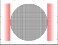 b)
b) 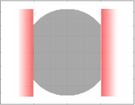
With the possibility of controlling of the DRN–lead coupling we can study how the energy spectrum and the wave functions are affected by attaching the leads. This is important because the wave functions are needed to calculate microscopically the tunneling matrix element between states in the DRN () and in leads ()
| (3) |
where the integration is performed over a surface separating the DRN and the leads. Within the Bardeen approach Bardeen ; Tersoff ; Tersoff1 ; Chen ; Chen1 it is assumed that and are eigenfunctions of the DRN and the leads, respectively. However, when the coupling gets stronger the real wave functions are modified and the Bardeen approach is not valid any more. Below we will show how increasing coupling affects the wave functions and how it affects conductivity.
But first we want to demonstrate the possibility of wave function engineering in a DRN. By this term we mean the ability to control the spatial distribution of the electron wave function by changing the shape of the confining potential. It is possible to control many of the potential parameters but here we will show the effect of tuning of the position of the QD potential . It can be realized by electrical gating below or above the central part of the DRN. Figure 3 shows the distribution of the ground state wave function for three different values of . With increasing position of the bottom of the QD potential the wave function is moved over from the QD part to the QR part of the DRN.
a)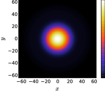 b)
b) c)
c)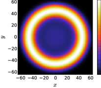
The wave functions have been calculated within the approach no. 1, i.e., by solving the Schrödinger equation only for the radial part . For all values of the state with and is the ground state. One can see that for the ground state wave function is located in the QD part of the DRN. Then, the wave function is pushed towards the ring part of the DRN with rising the bottom of the QD potential. The ground state wave function has a constant phase and its shape is exactly the same in all three mentioned above approaches. The situation can be different for excited states. Moreover, the spatial distribution of the wave functions can be significantly affected by even a very weak coupling to leads. We start the comparison of the wave functions calculated within different approaches with the case without leads. Since the ground state in all these methods is almost exactly the same, we start with the excited states. In Fig. 4 one can see the first (), the second () and the third () excited states (the second and third are degenerated) calculated within approach no. 1, where the full (complex) wave function is given by Eq. (2). These states were calculated for meV and . By comparing with Fig. 3a one can infer that these states can be located in a different part of the DRN than the ground state. As a result the matrix element between these states and the ground state is small and in Ref. zipper, ; MK0, we have demonstrated that this feature can be used to increase the relaxation time for a spin qubit built on a DRN.
a) b)
b) c)
c)
d)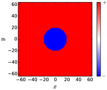 e)
e) f)
f)
Fig. 5 shows the same states calculated by solving the Schrödinger equation discretized in two dimensions and then diagonalized with the help of the Lanczös method (approach no. 2). In this case the wave functions are real.
a)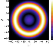 b)
b) c)
c)
d) e)
e)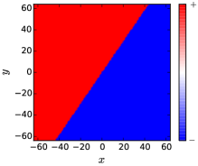 f)
f)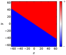
In this approach the cylindrical symmetry is broken by the discretization of the Schrödinger equation. Therefore and are not good quantum numbers any more. Of course, the second and the third excited states are still degenerated. One can check that these wave functions can be expressed as a linear combination of and (up to a phase factor, see Figs. 4b,e and 4c,f):
| (4) | |||||
| (5) |
Excited states calculated from the tight–binding model (approach no. 3) are resented in Fig. 6.
a) b)
b)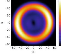 c)
c)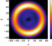
d)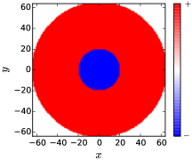 e)
e)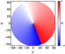 f)
f)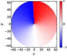
The wave functions are complex (like in approach no. 1), but the cylindrical symmetry of the Hamiltonian is broken (like in approach no. 2). The first excited state, which possesses (at least approximately) the cylindrical symmetry is the same in all the approaches. However, in the next two states the amplitude of the wave functions is angle–dependent, but the modulation is much weaker than in approach no. 2. Namely, the wave functions do not have nodes in any direction and therefore their phase cannot change discontinuously like in approach no. 2. What is interesting, this holds true only for an insulated system. If the system is even very weakly coupled to leads, the wave functions become real with nodes, like in approach no. 2. Such situation is presented in Fig. 7.
a) b)
b)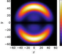
c)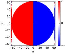 d)
d)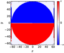
If the coupling is very weak, it only breaks the underlying cylindrical symmetry of the original Hamiltonian but the character of the states remains unaffected. The degeneracy of the second and the third excited states shown in Fig. 7 corresponds to the degeneracy of states and . However, when the coupling increases the change of the geometry becomes important and the spatial distribution of the wave functions changes as well. The changes are pronounced mainly for states which are located in the ring part of the DRN, i.e., close to the areas where the leads are attached. Fig. 8 demonstrates how the ground state for meV (which even in the absence of coupling to leads is located entirely in the QR) evolves with increasing coupling.
a) b)
b)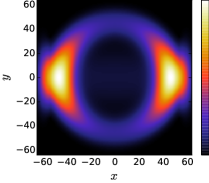 c)
c)
One can see there that in the case of strong coupling the wave functions are completely different from these in an insulated system and therefore in this regime the Bardeen approach cannot be valid. In order to determine the regime where this approximation can be used, in the next section we compare the coupling constants and conductivities calculated within the Bardeen approach and with the help of the Kwant package for a tight–binding model.
III The dot–ring nanostructure with leads
In this section we study a system composed of the DRN and weakly coupled source and drain leads with and as the subsequent tunneling rates. We focus here on the case of equal tunnel barriers, i.e., . Within the first method we calculate the tunnel rate for tunneling through state as
| (6) |
where is given by Eq. (3). In the following we restrict our study only to tunneling through the ground state () and skip the indices “00” in . Note that the situation where only the ground state is in the bias window not always can be realized because for some values of energy levels cross.
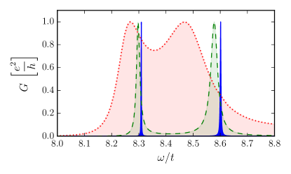
Since package Kwant does not allow one to calculate the tunneling rates directly, we use the Breit-Wigner formula BW ; BW1 ; BW2 for the energy-dependent transmission that gives the half–width–at–half–maximum of the conductance peak equal to :111Our studies are restricted to low temperatures so the thermal broadening of the conductance peak can be neglected.
| (7) |
This fit, however, works only for separate peaks in a system with relatively weakly coupled leads. Fig. 9 shows how well the Breit-Wigner formula describes the conductance peak in this regime.
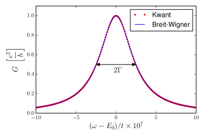
For a stronger coupling, when the peak broadening is so large that adjoining peaks overlap with each other, this formula does not give good results.
In Fig. 10 we show a comparison of the tunneling rate between a lead and the ground state calculated with the help of the Bardeen approach [Eqs. (3) and (6)] and determined from the width of the conductance peak.
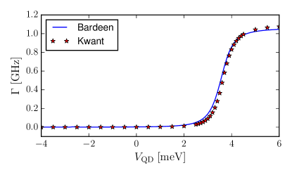
One can see there that as far as is small, the ground state wave function is located in the QD part of the DRN (situation presented in Fig. 3a) and there is no coupling to the leads. When the bottom of the QD potential is sufficiently high the wave function moves over towards the QR part (Fig. 3b) and the coupling increases. For meV the wave function is entirely in the QR and further increase of does not affect its shape (Fig. 3c). As a result saturates. In the case presented in Fig. 10 the leads where attached at a finite distance from the DRN (see Fig. 2a) so the height of the barrier between the nanosystem and the lead was almost . Fig. 11 shows the cross section of the confining potential along the axis.

For such a high barrier the coupling is weak independently of the distribution of the wave function. Fig. 10 shows that even if is so large that the wave function is located only in the outer (QR) part of the DRN, calculated within the framework of the Bardeen approach remains in a good agreement with the tight binding model that takes into account modifications of the wave function shape due to attached leads.
However, as the distance between the lead and the DRN decreases, the tunneling barrier becomes smaller and the DRN energy spectrum and shape of the wave functions change. Fig. 12 presents how the spectrum changes when the lead is shifted towards the DRN.
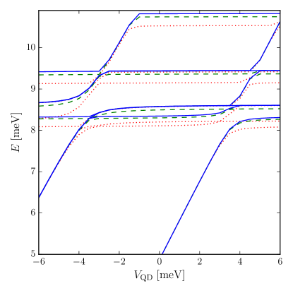
The energy levels in some regimes linearly increase with increasing and in others are almost constant. Since describes the confining potential only in the QD part of the DRN, whereas its shape in the QR parts is constant, states with energies that depend on are located mostly in the central QD. Fig. 12 shows that the energies of these states are not affected by attaching leads, even if the coupling is relatively strong. On the other hand, the states with energies independent of are located in the QR, where their matrix elements with states in the leads are finite and increase with increasing coupling. As a result their energies do depend on the position of the leads. As shown in Fig. 8 not only the energies, but also the shapes of the wave functions are modified in this regime. Both the effects, i.e., the reduction of the tunnel barrier between the DRN and the leads together with the change of the distribution of the wave function, lead to a dramatic increase of the coupling between the states in the DRN and in the leads. The resulting change of the tunneling rates is presented in Fig. 13.
IV Summary
Combined quantum structures are highly relevant to new technologies in which the control and manipulations of electron spin and wave functions play an important role. In contrast to real atoms, DRNs allow for flexible control over the confinement potential which gives rise to wave function engineering. We have shown that the peculiar structure of a DRN allows us to use an electrical gating to manipulate the confinement potential so that the coupling between states in the DRN and in the leads can be changed by orders of magnitude. As a result, by applying the gate voltage one can easily control the conductance of a DRN. The difference between the “traditional” single electron transistor SIT and the DRN is that in our case the Coulomb blockade is not used. Instead, the gate voltage is used to switch it by coupling/decoupling of the DRN to/from the leads IJZ .
We have shown that in the case of weakly coupled leads the approximate cylindrical symmetry of the confining potential can be utilized and the Schrödinger equation for only the radial part of the wave function can be solved numerically. Then, the Bardeen method can be used to calculate microscopically the geometry–dependent transport properties. However, when the coupling to leads is stronger, the cylindrical symmetry of the wave functions is broken and other computational methods must be used. In this paper we have demonstrated that one of the possibilities is package Kwant, which allows one to do the required calculations relatively easily.
In this paper we have presented the case of sequential tunneling with only a single state in the bias window. From Fig. 12 one can infer that for some shapes of the confining potential energy levels are very close and such an assumption cannot be fulfilled. When more than one state is in the bias window and all the states are coupled to the leads, charge transport can take place through many states. Then, even if we still assume a single electron transport (the Coulomb blockade does not allow for more than one occupied state to be in the bias window), one has to take into consideration the relaxation processes between different states. Such situation has been analyzed in Ref. MK2, . The situation becomes much more complicated when more than one electron can occupy the DRN. In this case the Coulomb interaction and the spin degrees of freedom come into play, what gives a possibility to control other properties of the nanosystem. Then, a DRN may turn out to be useful also in spintronics. The work along this line is in progress and the results will be published elsewhere krakow .
Acknowledgment
This work was supported by the National Science Centre (NCN) grant DEC-2013/11/B/ST3/00824.
References
- (1) R. Hanson, L. P. Kouwenhoven, J. R. Petta, S. Tarucha, and L. M. K. Vandersypen, Rev. Mod. Phys. 79, 1217 (2007).
- (2) E. Zipper, M. Kurpas, and M. M. Maśka, New J. of Phys. 14, 093029 (2012).
- (3) M. Kurpas, B. Kędzierska, I. Janus-Zygmunt, M. M. Maśka, and E. Zipper, Acta Phys. Pol A 126, 20 (2014).
- (4) M. Kurpas, E. Zipper, and M. M. Maśka, "Engineering of Electron States and Spin Relaxation in Quantum Rings and Quantum Dot-Ring Nanostructures" in "Physics of Quantum Rings", Vladimir M. Fomin (editor), Springer 2014, p. 455
- (5) M. Kurpas, B. Kędzierska, I. Janus-Zygmunt, A. Gorczyca-Goraj, E. Wach, E. Zipper, M. M. Maśka, J. Phys.: Condens. Matter 27, 265801 (2015).
- (6) E. Zipper, M. Kurpas, J. Sadowski, and M. M. Maśka, J. of Physics: Condensed Matter 23, 115302 (2011).
- (7) Z. Zeng, C. S. Garoufalis, and S. Baskoutas, Phys. Lett. A 378, 2713 (2014).
- (8) J. Bardeen Phys. Rev. Lett. 6, 57 (1961).
- (9) J. Tersoff and D. R. Hamann, Phys. Rev. Lett. 50, 1998 (1983).
- (10) J. Tersoff and D. R. Hamann, Phys. Rev. B 31, 805 (1985).
- (11) C. J. Chen, Phys. Rev. B 42, 8841 (1990).
- (12) C. J. Chen, Phys. Rev. Lett. 65, 448 (1990).
- (13) T. B. Boykin and G. Klimeck, Eur. J. Phys. 25, 503 (2004).
- (14) Ch. W. Groth, M. Wimmer, A. R. Akhmerov, and X. Waintal, New J. Phys. 16, 063065 (2014).
- (15) B. Szafran, F. M. Peeters, S. Bednarek, Phys. Rev. B 70, 125310 (2004).
- (16) C. Somaschini, S. Bietti, N. Koguchi, and S. Sanguinetti, Nanotechnology 22, 185602 (2011).
- (17) C. Somaschini, S. Bietti, N. Koguchi, and S. Sanguinetti, Appl. Phys. Lett. 97 203109 (2010).
- (18) B. V. Numerov, Monthly Notices of the Royal Astronomical Society 84, 592 (1924); B. V. Numerov, Astronomische Nachrichten 230, 359 (1927).
- (19) A. D. Stone and P. A. Lee, Phys. Rev. Lett. 54, 1196 (1985).
- (20) M. Büttiker, Phys. Rev. B 33, 3020 (1986).
- (21) M. Büttiker, IBM J. Res. Dev. 32, 63 (1988).
- (22) M. A. Kastner Rev. Mod. Phys. 64 849 (1992).
- (23) I. Janus-Zygmunt, B. Kędzierska, A. Gorczyca-Goraj, M. Kurpas, M. M. Maśka, and E. Zipper, Acta Phys. Pol. A 126, 1171 (2014).
- (24) A. Biborski, A. P. Kądzielawa, A. Gorczyca-Goraj, E. Zipper, M. M. Maśka, and J. Spałek, to be published.