Refractive Index of p-SnS Thin Films and its Dependence on Defects
Abstract
Tin sulphide thin films of p-type conductivity were grown on glass substrates. The refractive index of the as grown films, calculated using both Transmission and ellipsometry data were found to follow the Sellmeier dispersion model. The improvement in the dispersion data obtained using ellipsometry was validated by Wemple-Dedomenico (WDD) single oscillator model fitting. The optical properties of the films were found to be closely related to the structural properties of the films. The band-gap, its spread and appearance of defect levels within the band-gap intimately controls the refractive index of the films.
1 Introduction
Tin sulphide (SnS) is an earth-abundant, non-toxic, inorganic semiconductor material having layered structure. Its structural and optical properties can be easily varied according to the methods of fabrication [1]- [3]. Literature shows that the SnS thin films can have both direct and indirect band-gaps ranging from 1.1-2.1 eV [4, 5]. Also, SnS can be of both p-type and n-type [6, 7]. All these properties make it a suitable as a photo-active layer in solar cells [8, 9], in near IR detectors [10] and as an optical data storage media [11].
Considering all these applications are based on the optical/ refractive index properties of SnS films, this paper addresses itself on the variation of the optical properties of SnS thin films with film thickness. Also, in our recent study on as grown SnS thin films (thickness between 450-960 nm), we observed persistent photocurrent (PPC) which decayed exponentially/ near exponentially with time [12]. We indicated that the variation in the time decay constant and in general the nature of decay might be associated with defect energy levels within the band-gap. The presence of defect energy levels (both acceptor and donor levels) within the band-gap is well documented in the literature [9, 13]. Due to the large atomic size of Sulphur, one does not expect interstitial defects [14]. Tin (Sn) vacancies are more predominant resulting in acceptor levels in SnS thin films [15] while donor levels appear due to sulphur vacancies within the lattice [16]. The present papers quest is not only to investigate the optical properties of p-SnS thin films of thicknesses 450-960 nm, but also to use the data to co-relate it with the PPC results of our previous studies.
2 Experimental
Tin sulphide thin films of varying thicknesses were grown at the rate of 2 nm/sec on glass slides by thermal evaporation technique. Pellets of SnS powder (99% purity) supplied by Himedia (Mumbai) were evaporated in vacuum better than Torr using a Hind High Vac (12A4D) thermal evaporation coating unit maintained at room temperature. Hotspot method confirmed the p-type conductivity of the as-grown films. Thickness of the films was measured using Vecco Dektak Surface Profiler (150) and the standard structural characterization of the films was done using Bruker D8 X-ray diffractometer. UV-VIS double beam spectrophotometer (Systronics 2202) was used for optical characterization of the films. The surface morphology of the samples was studied using a Field Emission-Scanning Electron Microscope (FE-SEM FEI-Quanta 200F). Spectroscopic Ellipsometry (SE) studies of the samples were done using J.A. Woolam (USA) spectroscopic ellipsometer at an angle of incidence of . Photoluminescence studies were done using Shimadzu’s spectrofluorophotometer Rf-5301PC at an excitation wavelength of 550 nm in the wavelength range of 300-1000 nm.
3 Results and Discussion
3.1 The Structural Analysis
Tin sulphide films in the thickness range of 450-1000 nm were used in this study. The discussion on refractive index would justify the appropriateness of the selection. X-ray diffraction studies of all the as-grown films without exception were nano-crystalline in nature with 450 nm thick sample having an intense peak around while all other samples had a lone intense peak around (fig 1). Fig (1) is of a 960 nm thick film and is representative for all the samples. The peak positions (both intense and smaller peaks) matched the peak positions as listed in ASTM Card No. 79-2193. This suggests that our samples have an orthorhombic unit-cell structure with lattice parameters , and . The peak around corresponds to the (005) plane while the peak at of the remaining samples was broad with a shoulder visible on enlarging the graph. This broadening of the peak was due to the very close, yet resolvable peaks, corresponding to the (113) plane () and (200) plane (). Fig (1) also shows the deconvolution of this broad peak. The deconvolution was done using standard software (Origin 6.0). Considering that deconvolution gives us the true Full width at half maxima (FWHM) of the Lorentzian XRD peaks, we can now calculate the average grain size of the as-grown films using the Scherrers formula [17]
| (1) |
where ‘D’ is the average grain size, is the wavelength of the X-ray used (), is Full Width at Half Maximum intensity of the diffraction peaks and is the Bragg’s angle. The 0.9 coefficient is used for spherical grains, as was the case with our samples (inset of Fig 2 shows spherical grains uniformly dispersed on sample surface). Fig (2) shows a linear increase in average grain size proportional to the film thickness, suggesting an improvement in crystallinity of the films with a corresponding increase in the film thickness. However, the 450 nm thick film did not follow the trend. We believe this might be due to a different orientation of the planes compared to the other samples considering its very low film thickness.
3.2 Optical Properties
To study the optical properties of the films, absorption and transmission spectra of the samples were analyzed in the wavelength range of 300-900 nm. The refractive index and band-gap of the films were calculated using the transmission and absorption data respectively. In the following passages we discuss our observations.
3.2.1 Band-gap Variation
The band-gaps of the as-grown films were evaluated from the absorption spectrum using the standard Tauc method [18]. Band-gap can be estimated by extrapolating the linear part of the plot between and , where ‘’ is the absorption coefficient and has its usual meaning. The variable ‘n’ takes the value of 2 or 0.5 for direct or indirect band-gap material, respectively. Although SnS is reported to have both indirect and direct band-gaps, we obtained linear fits for n=2 (fig 3A), suggesting that our p-SnS as-grown films without exception had allowed direct band-gap [19]. The band-gaps obtained for our samples are listed in Table I. It may be noticed that there is no or minor variation in the band-gap for the samples under study.
The exponential region of the absorption spectra gives information on the localized states that tail off from the band edge within the band-gap, usually called as Urbach energy (). It arises due to structural defects in the crystalline material [20, 21]. In this region, the absorption coefficient, ‘’, is given as
can be evaluated from the plot between and (fig 3B). It was found that increased linearly with film thickness (fig 4). The significance of this result would be discussed in the following section.
3.2.2 Refractive Index
Refractive Index of a thin film can be obtained from their transmission spectrum using the standard Swanepoel’s method [22, 23]. Swanepoel’s method involves drawing envelopes (fig 5) connecting the extreme points of the interference fringes appearing in the spectrum. Refractive Index in the transparent region is given as:
| (2) |
| (3) |
where, n is the refractive index of the film, is the minima of the interference fringes and ‘s’ is the refractive index of the substrate (which in our case is glass and is taken as 1.5).
Interestingly, the fringes did not appear in very thin (thickness less than 450 nm) and very thick samples (thickness greater than 870 nm), giving context to our thickness range selection. In thicker samples, it seemed as if the fringes were moving to higher wavelengths (). This was observed by Yue et al [24] too. Since Swanepoel’s method can not be applied in the spectra where fringes are absent, it restricts the film thickness on which calculations can be done and this presents as a major drawback of the method. In such cases, other methods like ellipsometry have to be employed for estimating the refractive index. Due to lack of fringes in thicker samples and limitations imposed by the technique, we report the variation of refractive indices seen in just three of our samples, namely 450, 650 and 870 nm thick films (inset ‘A’ of fig 5).
The refractive indices of SnS thin films showed normal dispersion relation i.e. it decreased with increasing wavelength. In fact the trend followed the Sellmeier relation [25] (curve fits have co-relation of 0.998)
| (4) |
It should be noted that while our data clearly showed that the refractive index of p-SnS films fit Sellmeier’s model, previous works have reported that the SnS follows Cauchy’s dispersion relation [26] and Wemple-DiDomenico single oscillator model (WDD) for refractive index [27]. Sellmeier model pictures each interband optical transistion as individual dipole oscillators such that one oscillator dominates and all the other oscillators are combined together into and represented by the coefficient ‘A’ [28]. Table II gives the coefficients of eqn (4) that fit to the experimental results. An increasing value of coefficient ‘B’ with film thickness suggested that the refractive index of the samples increased with film thickness for all wavelengths which is validated by inset ‘B’ of fig 5, which shows an increase in ‘n’ values with film thickness for two wavelengths, 750 and 850 nm.
Sellmeier model gives an empirical formula and fails to give an insight about the physical/ structural properties of the film. WDD model is an improved dispersion model as it relates the optical properties with internal structure by single electron oscillator approximation [29]. WDD model is represented by the following equation [30]
| (5) |
The WDD model gives a physical interpretation about the sample through these constants and , where ‘’ is the average band-gap parameter also known as the oscillator energy and is proportional to the material’s band-gap () and ‘’ is the dispersion energy. is a measure of inter-band oscillation strength and is given as
| (6) |
where ‘’ depends on the type of bond within the material ( for ionic bonding and 0.37 eV for co-valent bondings). ‘’ is the coordination number or the number of nearest neighboring cations, ‘’ is the anion valency, while ‘’ is the effective number of valence electrons per anion. We used the refractive index data obtained by Swanepoel’s method above and found that the data did not fit into WDD model equation given by eqn (5). Considering that the refractive index values strongly depend on the drawn envelopes in Swanpoel method, one should not be surprised by the inconsistent results.
Refractive index of films can also be determined by ellipsometry. Banai et al [31] have highlighted that spectroscopic ellipsometry (SE) combined with UV-visible spectroscopy can yield more accurate results for optical properties. Also, since only a few literature is present [32] on ellipsometry studies of SnS due to the difficult data analysis involved, we decided to augment our results by carrying out SE studies on our SnS samples.
The SE studies were done on our SnS films. Data of and collected were fit using two layer model, i.e. of film with finite thickness on semi-infinite glass substrate. The optical parameters, n and k, of the glass substrate used in these calculations were also evaluated using SE data. The problem of back scattering was taken care of by roughening the lower surface of glass substrate. The refractive index of the glass substrate was found to follow the Cauchy’s dispersion relation [33]
The program iterated different values of Sellmeier model’s constants and film thickness for the SnS layer till a small value of Mean Square Error (MSE) was obtained showing good convergence between fitted and experimentally obtained data (see fig 6). The constants of Sellmeier model obtained by SE data analysis are reported in Table III. As can be seen from fig (6), the data are oscillatory for and a good fit was not obtained, indicating that refractive index did not follow the Sellmeier dispersion model below 700 nm. Since we are interested in the transparent region, we had restricted ourselves for wavelength region (i.e. the region where Sellmeier applies). Unlike the refractive index data obtained by Swanepoel’s method, the refractive index obtained using SE was found to be decreasing with thickness. Fig (7) shows the variation of ‘n’ with film thickness for 750 and 850 nm wavelengths, a single straight line fitted for both the wavelengths due to minor variations in refractive index values at higher wavelengths where the Sellmeier model flats out. Also, these refractive index values were found to adhere to the WDD trend given by eqn (5). The perfect linear fit obtained with the SE data (see fig 8A) was an improvement over the results obtained using Swanepoel method, which failed to fit the linear trend (see fig 8B).
The prefect linear trend highlighted the accuracy of SE over Swanepoel method. The improvement in refractive index data obtained from SE over Swanepoel’s can be understood considering there are often discrepancies while deciding the strong transmission, weak-absorbing and strong absorbing region of the film’s absorption spectra on whose basis different formulae have to be applied. Also, ‘n’ is obtained by drawing envelopes for transmission graphs in the given wavelength range while in SE, ‘n’ is obtained by data fitting the model on two different variables ( and ). Thus, as the number of data fitting variable increases, the accuracy of the obtained refractive index values improves.
Table IV reports the values of and (eqn 5) evaluated from the graph (fig 8A). While the values of matched well with those of obtained using Tauc’s plot (literature reports ) [34], there was a stark variation in the values of as the film thickness varied. This was surprising considering that the XRD analysis and energy band-gap values suggested that the structure of the films were the same. However, the Urbach tail analysis suggested the presence of defects in the films, with increasing with the film thickness. We believe the variation in might be related to the defects in the films.
3.2.3 Photoluminescence
To investigate the presence of defect levels within the band-gap, PL measurements were made with the excitation wavelength of 550 nm. Fig (9) shows the observed PL spectra for all the films indicating a broad peak around (830-860 nm) which can be deconvoluted into two peaks. Since the band-gap of all the films was around 1.8 eV, these peaks could safely be associated with the radiative transitions from/to defect levels within the band-gap. Also, the presence of energy levels due to sulphur and tin vacancies in SnS are well documented and was also linked to the persistent photocurrent decay measurements of the as grown films [12].
Fig (10) gives a crude schematic energy band level diagram of the as grown SnS films. The two PL peaks correspond to the conduction band (CB) to acceptor level transition and donor level to acceptor level transition. Band-gap and donor to valence band (VB) transitions possibility were ruled out due the lack of peaks in PL corresponding to the expected energy levels. On co-relating our PL analysis with values, we find that increased as the energy difference between the donor and acceptor levels decreased (see fig 11). Physically this can be understood as the oscillation strength for the transition between the levels increases as the difference in the energy levels decreases. A similar trend was also seen between and of the Urbach tail (fig 12) which confirmed the intimate relation of with defect structures and energy levels introduced by it. Increase in with thickness indicated the increase in tailing or spread of the band edges (increase in width of the localized states within the band-gap) with thickness. Thus, validating our persistent photocurrent results [12] where thinner samples showed a single exponential decay curve due to small width of levels while as the width increased, multiple transition levels appeared and a non-exponential decay curve was observed.
4 Conclusions
Nano-crystalline p-type SnS thin films grown on microscopy glass slide by thermal evaporation at room temperature were studied. Their optical properties were found to be dependent on the film thickness in the range 450-1000 nm. The optical studies showed a band-gap of for the as-grown films with the width of localized states (Urbach’s tail) increasing with thickness. Swanepoel’s method was used for evaluating refractive index for films using interference fringes in their transmission spectra. Refractive index followed Sellmeier dispersion relation. The fitting coefficients were used as initial guess for ellipsometric studies of the as grown films. The improved dispersion data were validated by fitting WDD model, which indicated that the defect levels affect the refractive index of the film. The study also validated the PPC exponential decay for thinner and non-exponential decay for our thicker samples. Thus, the desired optical properties of the material can be obtained by material manuplication like changing thickness, grain size or introducing defect levels for use in various applications.
5 Acknowledgments
One of the authors (YG) acknowledges DST (India) for the financial support extended under the INSPIRE program (Fellowship No. IF131164).
References
- [1] K.N.Reddy and K.T.R.Reddy, Mater. Chem. Phys. 102, (2007) 13.
- [2] S.Kamoshida, S.Suzuki, S., Japan Patent JP 08176814, A2, 1996.
- [3] M.M.El-Nahass, H.M.Zeyada, M.S.Aziz and N.A.El-Ghamaz, Opt. Mater., 20 (2002) 159.
- [4] C. Gao, H. Shen, L. Sun, Appl. Surf. Sci. 257, (2011) 6750.
- [5] S. Sohila, M. Rajalakshmi, C. Ghosh, A.K. Arora, C. Muthamizhchelvan, J. Alloy Compd. 509, (2011) 5843.
- [6] O.E.Ogah,K.R.Reddy,G.Zoppi,J.Forbes,R.W.Miles, Thin Solid Films 519, (2011) 7425.
- [7] M.Leach,K.T.R.Reddy,M.V.Reddy,J.K.Tan,D.Y.Jang, R.W.Miles, Energy Procedia 15, (2012) 371.
- [8] C. Gao, H. Shen, Z. Shen, Mater, Lett 65, (2011) 1143.
- [9] H.Noguchi, A,Setiyadi, H.Tanamura, T.Nagatomo and O.Omoto, Sol. Energy Mater. Sol. Cells 35, (1994) 325.
- [10] T.H.Patel, The Open Surface Science Journal 4, (2012) 6.
- [11] G.H.Yue, W.Wang, L.S.Wang, X.Wang, X.Yan, Y.Chen, D.L.Peng, J. Alloy Compd 474, (2009) 475.
- [12] Y.Gupta, P.Arun, Phys. Status Solidi B, (2015) DOI 10.1002/pssb.201552249.
- [13] A.S.Juarez, A-Tiburcio-Silver,A.Orliz, Thin Solid Films, 480 (2005) 452.
- [14] Y.Wang,H.Gong,B.Fan,G.Hu,J. Phys. Chem. C, 114 (2010) 3256.
- [15] M.Ristov,G.Sinadinovski,J.Grozdanov,M.Mitreski, Thin Solid Films 173 (1989) 53.
- [16] T.H.Sajeesh, K.B.Jinesh,M.Rao,C.S.Kartha,K.P.Vijayakumar, Phys. Status Solidi A, 207 (2010) 1934.
- [17] B.D. Cullity, S.R. Stock, “Elements of X-Ray Diffraction”, Ed., Prentice-Hall Inc (NJ, 2001).
- [18] J.Tauc, Mat Res Bull 5, (1970) 721.
- [19] J.I.Pankove, “Optical processes in semiconductors” (NY: PHI, 1971).
- [20] A.Iribauen,R.Castro-Rodriguez,V.Sosa,J.L.Pena,Phys. Rev. B, 58 (1998) 1907.
- [21] A.C.Aragones,A.Palacios-Padros,F.Caballeco-Briones,F.Sanz, Electrochemica Acta 109 (2013) 117.
- [22] R.Swanepoel, J. Phys. E, Sci. Instrum. 16, (1983) 1214.
- [23] R.Swanepoel, J. Phys. E, Sci. Instrum. 17, (1984) 896.
- [24] G.H.Yue, D.L.Peng, P.X.Yan, L.S.Wang, W.Wang, X.H.Luo, J. Alloy Compd 468, (2009) 254.
- [25] H. Fujiwara, “Spectroscopic Ellipsometry-Principles and Applications”, John Wiley (NY 2007).
- [26] C. Cifuents, M. Botao, E. Romero, C. Caldero, G. Gordillo, Braz. J. Phys. 36, (2006) 1046.
- [27] H. Saraf, M. Merdan, O.F. Yuskel, Turk. J. Phys. 26, (2002) 341.
- [28] M.DiDomenico, S.H.Wemple, J Appl Phys, 40 (1969) 720.
- [29] W.Yang,Z.Zhou,B.Yang,Y.Jiang,H.Tian,D.Gong,H.Sun,W.Chen, Appl. Surf. Sci. 257 (2011) 7221.
- [30] S.H. Wemple, M. DiDomenico, Phys. Rev. B 3 (1971) 1338.
- [31] R.E.Banai, H.Lee, M.Lewinsohn, M.A.Motyka, R.Chandrasekaran, N.J.Podraza, J.R.S.Brownson and M.W.Jorn, DOI:10.1109/PVSC.2012.6317592
- [32] E.R.Shaaban, M.S.Abd.El-Sadek, M.El-Hagary, I.S.Yahia, Phys. Scri. 86, (2012) 015702.
- [33] Y.Gupta, P.Arun, Int. J. Phys., 3 (2015) 8.
- [34] M.S. Selim, M.E. Gouda, M.G. El-Shaarawy, A.M. Salem, W.A.A. El-Ghany, J. Appl. Res. 7 (2011) 955.
Figures
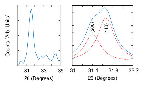
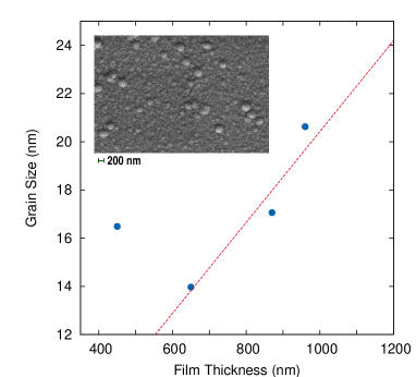
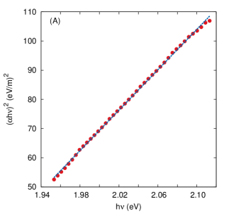
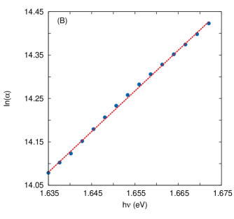
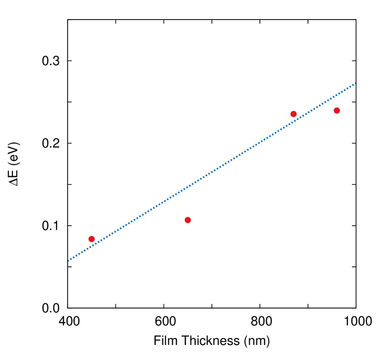
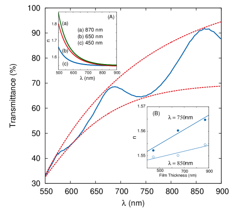
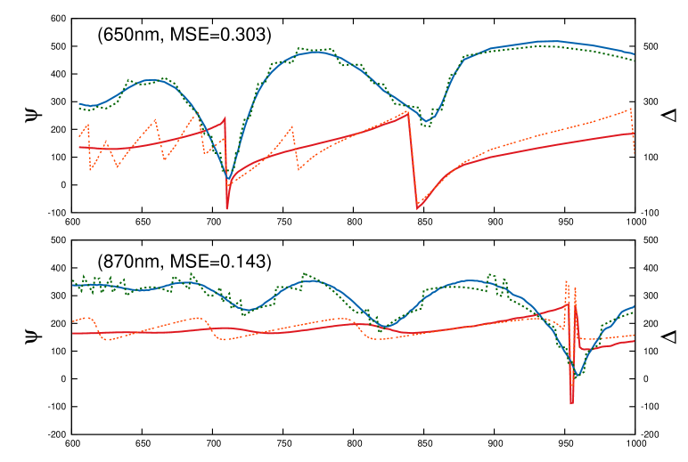
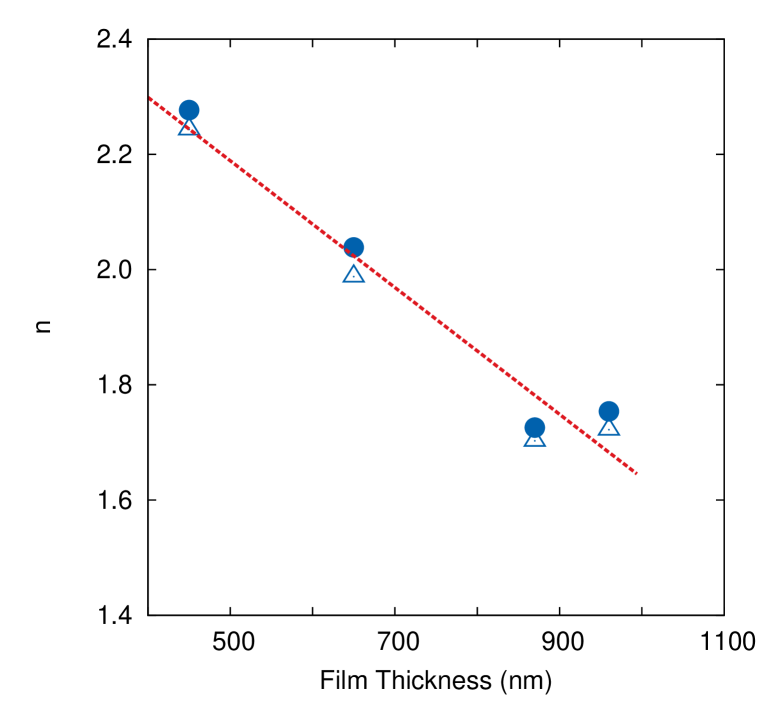
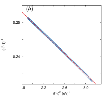
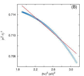
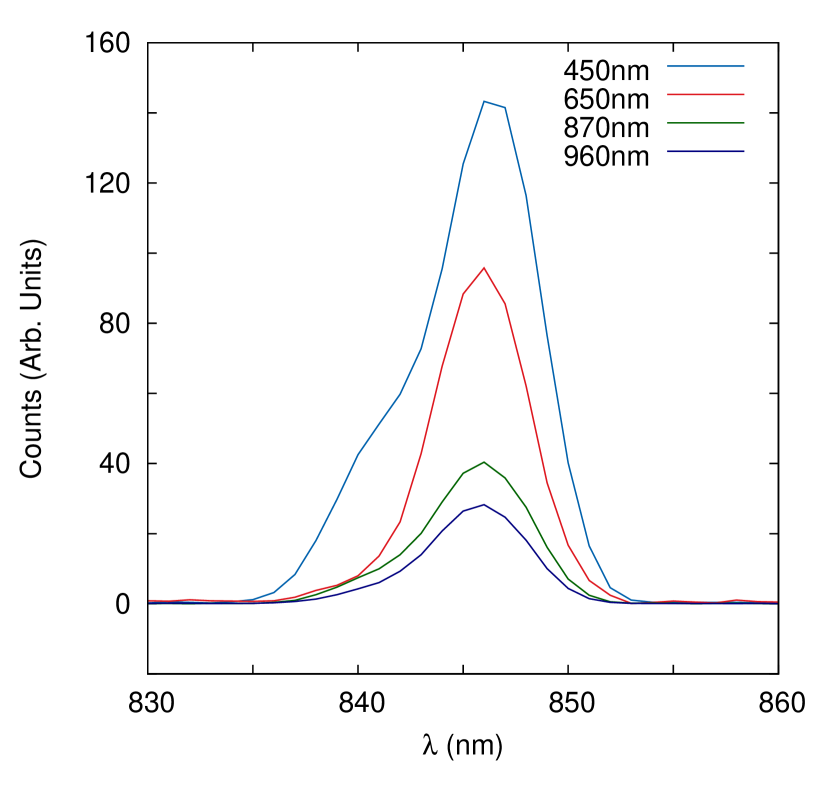

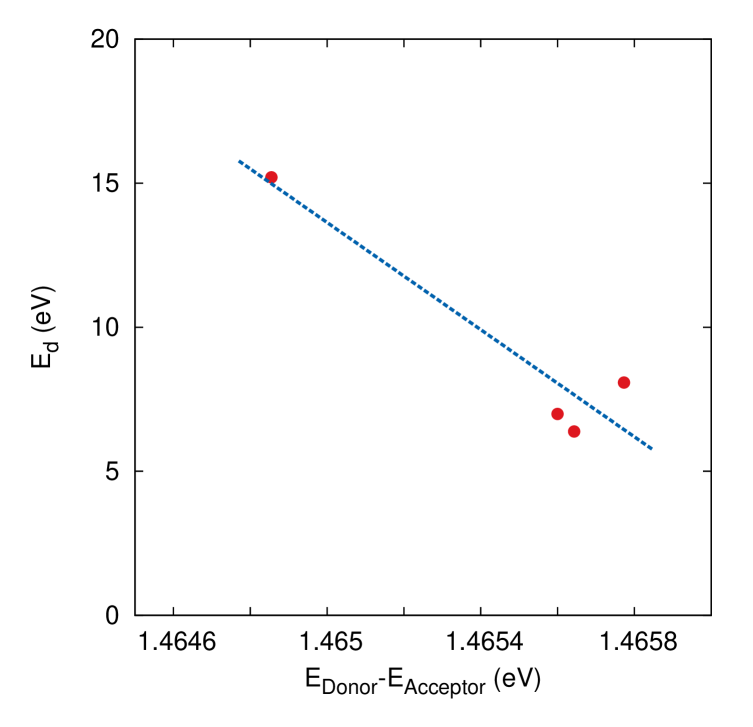
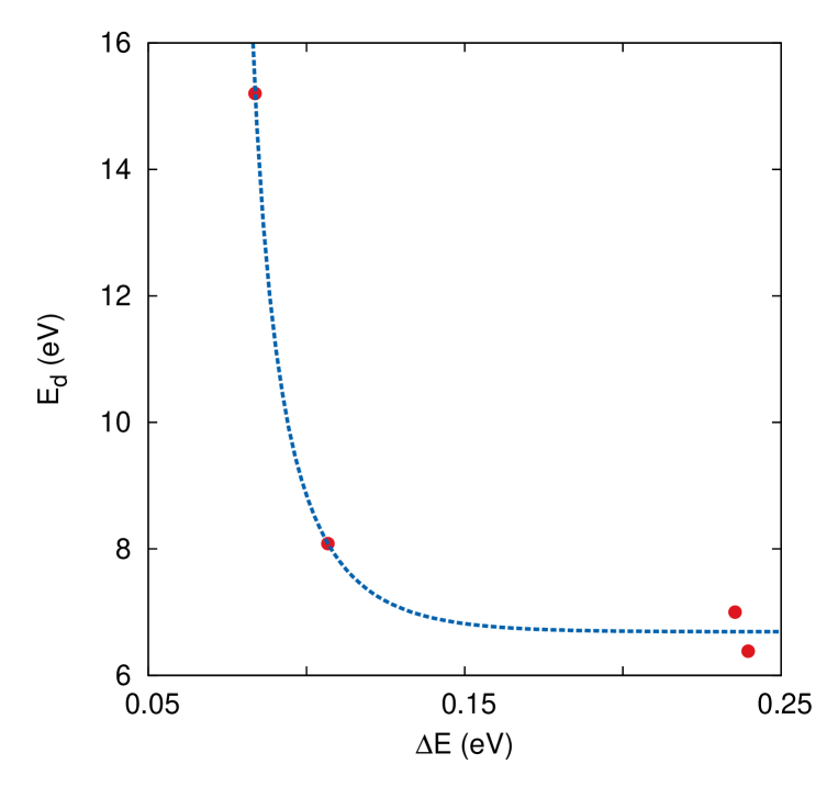
Figure Captions
-
1
X-ray diffractogram of film with thickness 960 nm. Plot showing deconvolution of broad peak at indicating (113) as the preferred orientation for 960 nm thick film.
-
2
Plot shows variation in average grain size with thickness for the as-grown films. Inset shows spherical grains seen by Scanning Electron Microscope. The micrograph exhibited here is of 870 nm thick SnS films.
-
3
Plot exhibits variation of (A) with for 650 nm thick film. Extrapolation of the best fit line to the X-axis at y=0 gives the band gap of the samples. Plot of (B) with for the same sample. The inverse of the slope gives the Urbach energy of the sample.
-
4
Variation of Urbach energy with film thickness.
-
5.
Transmission spectra of 450 nm thick film used to calculate refractive index by Swanepoel’s method. Dotted line shows the envelopes drawn joining the fringe maximas and minimas. Inset (A) shows the fit of Sellmeier’s model to the calculated refractive indices. Inset (B) shows the linear variation in refractive index with film thickness for wavelengths 750 and 850 nm.
-
6.
The experimental (solid line) and theoretically modelled (dotted line) spectra for the two ellipsometric parameters ( and ) for film thickness of 650 and 870 nm.
-
7.
Variation of refractive index obtained from SE with thickness for 750 nm (circles) and 850 nm (triangles) wavelengths.
-
8.
WDD model fitting for refractive index data obtained using (A) Ellipsometry data, (B) Swanepoel’s method. Slope (m) and intercept (c) were used to calculate and .
-
9.
PL spectra for the asgrown films.
-
10.
Basic energy level diagram of SnS showing the two possible radiative transitions corresponding to the peaks in PL spectra.
-
11.
Variation in dispersion energy () with the energy difference between donor and acceptor levels (calculated using PL data).
-
12.
Variation in dispersion energy () with Urbach energy ().
Table I: Band-gap values obtained for different film thicknesses using Tauc’s method.
| Film Thickness (nm) | Band-gap (eV) |
|---|---|
| 450 | 1.83 |
| 650 | 1.80 |
| 870 | 1.79 |
| 960 | 1.84 |
Table II: Constants of the Sellmeier model obtained via curve fit for different film thicknesses.
| Film Thickness (nm) | A | () | |
|---|---|---|---|
| 450 | 2.278 | 0.0834 | 2.08 |
| 650 | 1.983 | 0.3006 | 1.92 |
| 870 | 1.963 | 0.3180 | 1.99 |
Table III: Constants of the Sellmeier model obtained via SE data analysis for different film thicknesses.
| Film Thickness (nm) | A | () | |
|---|---|---|---|
| 450 | 2.2 | 2.4 | 1,1 |
| 650 | 2.4 | 1.1 | 2.1 |
| 870 | 2.0 | 0.7 | 1.6 |
| 960 | 1.9 | 0.8 | 1.8 |
Table IV: and obtained for various thicknesses.
| Film Thickness (nm) | ||
|---|---|---|
| 450 | 4.32 | 15.20 |
| 650 | 3.37 | 8.08 |
| 870 | 4.19 | 6.99 |
| 960 | 3.81 | 6.38 |