Materials properties of out-of-plane heterostructures of MoS2-WSe2 and WS2-MoSe2
Abstract
Based on first-principles calculations, the materials properties (structural, electronic, vibrational, and optical properties) of out-of-plane heterostructures formed from the transition metal dichalcogenides, specifically MoS2-WSe2 and WS2-MoSe2 were investigated. The heterostructures of MoS2-WSe2 and WS2-MoSe2 are found to be direct and indirect band gap semiconductors, respectively. However, a direct band gap in the WS2-MoSe2 heterostructure can be achieved by applying compressive strain. Furthermore, the excitonic peaks in both monolayer and bilayer heterostructures are calculated to understand the optical behavior of these systems. The suppression of the optical spectrum with respect to the corresponding monolayers is due to interlayer charge transfer. The stability of the systems under study is confirmed by performing phonon spectrum calculations.
Transition metal dichalcogenides (TMDCs) are promising materials for various applications Zhao ; Late ; Li1 ; Chhowalla ; Xu , for example field-effect transistors. Quantum confinement in these semiconductors going from bulk to monolayer results in the transition from indirect to direct band gap semiconductor, which makes them superior in nano-electronics applications as compared to the well studied material graphene that has no band gap.Thanasis12 ; He14 ; santosh1 ; deep ; santosh3 ; hu ; santosh2 ; mak ; santosh4 In addition, due to their distinct electronic properties, TMDC monolayers have been utilized in logic circuits Radisavljevic11 as well as in memory devices.Simone13
Stacking of TMDCs monolayers in order to form heterostructures with van der Waals interactions enables the creation of atomically sharp interfaces Hong14 , and also provides a route to a wide variety of semiconductor heterojunctions with interesting properties.Yongji14 Type-II band alignment in these heterostructures has been demonstrated, which reduces the overlap between the electron and hole wave functions by slowing down the charge recombination, which in fact is expected to be an efficient way for light detection and harvesting.Hong14 ; Riya Recently, the long-lived interlayer excitons have been investigated in the MoSe2-WSe2 heterostructure, which indeed opens the large avenue for light-emitting diodes and pholvoltaic devices.Rivera15 . The structural, electronic, photocatalytic, and optical properties of out-of-plane and in-plane heterostructures of TMDCs have been investigated by employing first-principles calculations.Amin15 It has been demonstrated that all the out-of-plane heterostructures show an indirect band gap with type-II band alignment. However, a direct band gap can be obtained by the application of tensile strain in specific cases, such as the heterostructures of MoSe2-WSe2 and MoTe2-WTe2. It has also been predicted by theoretical calculations that the direct band gaped bilayer can be generated by alteration of the individual monolayers of TMDCs in the heterostructures.Humberto13
A vertical heterostructure of MoS2-WSe2 has been fabricated by stacking of MoS2 and WSe2 monolayers.Chiu14 Based on the shifts observed in the Raman and photo-luminescence spectra, it has been found that thermal interactions enhance the coupling between the two monolayers. An atomically thin p-n junction diode has been synthesized from a stacked MoS2-WSe2 heterojunction. It shows an excellent current rectification and rapid photo-response with a high quantum efficiency.Cheng14 Lee et al. Lee14 also fabricated atomically thin p-n heterojunctions from MoS2 and WSe2 monolayers and demonstrated that the tunneling-assisted coupling between MoS2 and WSe2 layers is responsible for the tunability of the electronic and optoelectronic responses. The van der Waals heterostructures of MoS2-WSe2 and MoS2-MoSe2 have been demonstrated using ultra-low frequency Raman spectroscopy.Chun It has been shown that a special Raman feature arises from the layer-breathing mode vibration between two incommensurate monolayers. Due to the charge transfer across the interface of the MoS2 and WSe2 heterostructures, a photovoltaic effect has been observed.Furchi15 Furthermore, a high gate coupling efficiency of about 80% has been demonstrated for tuning the band offsets at the MoS2-WSe2 vertical interface in dual-gate device.Tania15
However, the structural and electronic properties of such heterostructures are not well understood. Therefore, in the present work, comprehensive insight is gained into the physical properties of the MoS2-WSe2 and WS2-MoSe2 heterostructures that are investigated with/without biaxial compressive strain using density functional theory calculations (see supplementary material).supp The reduction of the optical spectrum with respect to the corresponding monolayers is analyzed. Furthermore, the stability of the systems under consideration is confirmed by means of the phonon spectrum.
| MoS2-WSe2 | WS2-MoSe2 | MoS2-WSe2 | WS2-MoSe2 | |
|---|---|---|---|---|
| PBE | HSE06 | |||
| a (Å) | 3.25 | 3.25 | 3.22 | 3.22 |
| 3.37 | 3.36 | 3.33 | 3.34 | |
| X–S (Å) | 2.43 | 2.43 | 2.40 | 2.40 |
| X–Se (Å) | 2.53 | 2.52 | 2.50 | 2.50 |
| (eV) | -0.20 | -0.21 | -0.24 | -0.25 |
| (eV) | 0.33 | 0.87 | 0.94 | 1.58 |
| (eV) | 0.46 | 0.19 | 0.44 | 0.18 |
| (eV) | 0.003 | 0.019 | 0.026 | 0.035 |
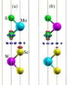
The out-of-plane heterostructures were created by using the average of the experimental lattice constant of the constituent monolayers and by keeping one layer on top of the other such that the S/Se atoms of one layer sit on top of the W/Mo of the other layer Humberto13 , see Fig. 1. We have also cross-checked the heterostructures by using the lattice parameters of the constituent monolayers individually. After the relaxation of both the lattice constant and positions, the lattice parameter optimized to the average value of the corresponding monolayers, as summarized in Table I. In principle, the PBE calculations overestimate, while HSE06 calculation give the correct value to the average of the experimental lattice constant of individual monolayers in corresponding heterostructures.apl Hence, after relaxation the MoSe2 and WSe2 monolayers suffered from 1.8% compressive strain, while the MoS2 and WS2 monolayers suffered from the same amount of tensile strain in agreement with Ref. Chiu14 . The obtained value of the interlayer spacing agrees well with experimentally and theoretically obtained values for heterostructures made of MoS2 and WS2 and graphene and WS2 or WSe2.kaloni-apl ; ncom The calculated bond lengths presented in Table I for both MoS2-WS2 and WS2-MoSe2 agree well with those of the corresponding monolayers (Ref. Kang13 ) inferring weak van der Waals interactions between monolayers in the heterostructures.
The binding energies were obtained as , where (X=S, Se) is the total energy of the heterostructure, and and are the total energies of the corresponding monolayers. The calculated binding energies presented in Table I show that the out-of-plane heterostructures have negative binding energies, which confirms that these systems are energetically favorable.
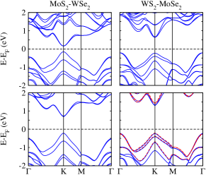
The band structures presented in Fig. 2 show that the heterostructure MoS2-WSe2 is a direct band gap semiconductor, while WS2-MoSe2 is found to be an indirect band gap semiconductor.Humberto13 Normally, the PBE functional underestimates the band gap, therefore, the HSE06 functional is used since it has already been demonstrated that the HSE06 functional provides correct value of the band gap in terms of experimental observation.apl The band structures shown in Fig. 2 indicate the direct and indirect band gap nature of the heterostructures of MoS2-WSe2 and WS2-MoSe2, respectively. The indirect band gap nature of the WS2-MoSe2 heterostructure is due to the fact that the valence band maximum (VBM) is contributed by the Mo atom, for which the spin-orbit splitting is smaller because of lower atomic number as compared to the W atom. Thus, the VBM lies at the -point of the Brillouin zone.
To understand the contributions from different atomic sites, we have investigated the weighted band structure of both the heterostructures of MoS2-WSe2 and WS2-MoSe2. It is clear from Fig. 3 that the conduction band minimum (CBM) at the K-point is due to the Mo orbital and the VBM at the K-point is due to the W and W orbitals of the MoS2-WSe2 heterostructure. This localization of the VBM and CBM in different monolayers physically separates the electron hole pairs. The strong coupling between the S/Se orbitals and Mo/W and orbitals leads to a large splitting between their bonding and anti-bonding states, hence these orbitals do not contribute to the band edges. These results show that the VBM and CBM are contributed from different monolayers. This type of arrangement where the holes and electrons are attributed to different layers is known as type-II band alignment.Hong14 The homogeneous bilayers of TMDCs do not possess this net charge separation, so that an external electric field is required to achieve a type-II band alignment Ashwin11 . However, there is no electric field in our calculations for the heterostructures that nevertheless show type-II band alignment, which may be due to the intrinsic electric field that arises due to the buckled structures.k1 ; k2 ; k3
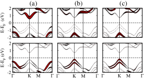
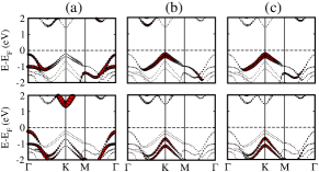
In contrast to the MoS2-WSe2 heterostructure, the CBM at the K-point of the WS2-MoSe2 heterostructure is due to the W orbital. Without applying strain, the VBM is at the -point, and it is also due to the W orbital with a major contribution from the Mo orbital. Hence, the heterostructure of WS2-MoSe2 possesses a type-I band alignment, in agreement with the prediction made by Ref. Hannu13 . Strain engineering is a widely used strategy to achieve tunable band gaps for two-dimensional materials. Amin14 Therefore, with the application of 0.5% compressive strain, the VB at the K-point shifts to higher energy, which is due to the Mo and Mo orbitals. Whereas, the VBM at the -point shifts to lower energies. Hence, both the VBM and CBM separate the electron hole pairs to different layers and change the material to the type-II band alignment, see Fig. 4. Due to their type-II band alignment, these heterostructures can be used as active materials for fabrication of heterojunction photovoltaic devices; type-II band alignment is usually required for charge separation or formation of junctions.Lee14
The strong spin-orbit coupling results in a significant valence band splitting () with a minute conduction band splitting (), see Table 1. The fact is that W contributes much more to VB than Mo, and hence the VB is split. The situation is reversed for the CB, resulting in a split that is very small only, see Fig. 3. The valence band splitting in the heterostructure of MoS2-WSe2 was found to be larger than that of pristine MoS2 monolayers ( 0.15 eV and =0.20 eV) Kang13 and smaller than that of the pristine WSe2 monolayers (=0.47 eV and =0.63 eV) Kang13 . The same behavior is found for the heterostructure of WS2-MoSe2. The splitting of the valence band (holes) and conduction band (electrons) indicates that the formation of the heterostructure is a promising route to engineer the band gap and splitting. These systems may therefore be interesting for optoelectronic and spintronic devices.Ochoa13
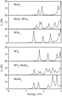
Further, the imaginary parts of the dielectric function of the monolayers and the heterostructures were calculated by solving the Bethe-Salpeter equation. The results presented in Fig. 5 show that the optical transitions are dominated by excitons. For monolayer MoS2, excitonic peaks are observed at 1.77 eV and 1.92 eV, while for monolayer WSe2 they appear at 1.50 eV and 1.96 eV. Similarly, these peaks appear at 1.77 eV and 2.24 eV for WS2, while at 1.48 eV and 1.72 eV for monolayer MoSe2. The position of the first excitonic peaks are in good agreement with the experimental values of MoS2 (1.85 eV), WSe2 (1.59 eV), WS2, and MoSe2 (1.56 eV).Chun ; Rivera15 ; Ashwin12 Fig. 5 shows a systematic red shift of the excitonic peaks as the chalcogen atom becomes heavier. In general, for the red shift the band gap decreases, while for the blue shift the band gap increases Trodahl . We obtain exciton binding energies of 1.05 eV for MoS2, 0.95 eV for WSe2, 1.04 eV for WS2, and 0.95 eV for MoSe2 monolayers. Strong modifications of the excitons in the heterostructures with respect to the parent monolayers were found, see Fig. 5. The excitonic peaks are shifted to 1.6 eV and 1.8 eV in the case of the MoS2-WSe2 heterostructure, in agreement with photoluminescence spectroscopy.Chun ; Furchi15 The remarkable decrease in the photoluminescence intensity of the heterostructures with respect to the parent monolayer has also been reported previously Chun ; Lee14 and is due to the efficient interlayer charge transfer. Note that, in the real experimental situation in the presence of dielectric medium, the position of an excitonic peak might change slightly.acs
The charge transfer rate is close to the rate of exciton generation. Due to the type-II band alignment, in case of the MoS2-WSe2 heterostructure the photoexcited electrons in the WSe2 layer tend to flow to the MoS2 layer, and the holes in the MoS2 layer tend to flow to the WSe2 layer. The spatial separation of the electrons and holes therefore suppresses the intralayer optical recombination processes and thus the optical spectrum. To investigate the charge transfer between the constituents monolayers of the heterostructures, the charge density difference was addressed (see Fig. 1); calculated as , where is the charge density of the heterostructure, is the charge density of the isolated MoX2 monolayer and is the charge density of the isolated WY2 monolayer. From the Bader population analysis we have fiound that the S atom gains 0.008 e, while the Se atom loses 0.012 e in the MoS2-WSe2 heterostructure. Similarly in case of WS2-MoSe2 Se atoms lose 0.009 e, while S atoms gain 0.016 e, where for unstrained system this amount is 0.009 e for Se and 0.005 e for S. These results are in good agreement with the available values reported in Ref. Xiangying14 , and show that the interlayer bonding of MoS2 and WSe2 should be rather weak and due to long-range van der Waals forces.
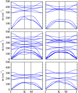
In Fig. 6, the calculated phonon spectra for the heterostructures of MoS2-WSe2 and WS2-MoSe2 show good agreement with the experimental data presented in Ref. Chiu14 In the case of the MoS2-WSe2 heterostructure the acoustic and optical vibration modes are at the same energies as for the corresponding monolayers of WSe2 and MoS2. This indicates once more that there are only very small van der Waals interactions between the two layers. The phonon spectra for pristine monolayers of both MoS2 and WSe2 were also calculated for comparison. The characteristic bands observed at 410 cm-1 and 380 cm-1 are in a good agreement indeed with the experimental values of 403 cm-1 and 385 cm-1 Chiu14 , which are due to the A1 mode (out-of-plane vibrations) and E1 mode (in-plane vibrations), respectively, of the MoS2 monolayer in the heterostructure. The bands at about 250 cm-1 to 260 cm-1 are due to the E1 and A1 modes of the monolayer of WSe2. These bands are also in good agreement with the experimental values of E1 (248 cm-1) and A1 (260 cm-1).Chiu14 The positions of these bands are also in agreement with those of the corresponding monolayers with a small red shift (shift to lower energy) with respect to isolated MoS2 and blue shift (shift to higher energy) with respect to isolated WSe2.Chiu14 Both of these blue and red shifts with respect to the corresponding monolayers are due to the fact that tensile strain is induced in MoS2 and compressive strain is induced in WSe2 while constructing the heterostructures. The characteristic peaks are well reproduced with respect to the experiments. Although these peaks are not exactly the same as those obtained in experiment, the simulation results provide a good approximation. The positions of the bands in the heterostructure of MoS2-WSe2 with respect to the corresponding monolayers show that the layers are decoupled having a very small van der Waals interaction.
In summary, we have investigated the structural and electronic properties and the vibrational and optical spectra of the van der Waals heterostructures of MoS2-WSe2 and WS2-MoSe2. It was found that MoS2-WSe2 is a direct band gap semiconductor with type-II band alignment. In contrast to the MoS2-WSe2 heterostructure, the WS2-MoSe2 heterostructure is an indirect band gap semiconductor with type-I band alignment. A compressive strain is an efficient way to change the heterostructure of WS2-MoSe2 from indirect to direct band gap nature with type-II band alignment. The splitting of the valence band (holes) and conduction band (electrons) indicates that the formation of the heterostructure is a promising route to engineer the band gap and band splitting, such that these systems would be interesting for optoelectronic and spintronic devices. The reduction of the optical spectrum with respect to the corresponding monolayers is analyzed and the stability of the systems under consideration is confirmed with the help of the phonon spectrum.
GS acknowledges funding from the Natural Sciences and Engineering Council of Canada (NSERC, Discovery Grant). MSF acknowledges support by NSERC, the Canada Research Chair program, Canada Foundation for Innovation (CFI), the Manitoba Research and Innovation Fund, and the University o f Manitoba.
References
- (1) Y. Zhao, Y. Zhang, Z. Yang, Y. Yan, and K. Sun, Sci. Technol. Adv. Mater. 14, 043501 (2013).
- (2) D. J. Late, Y.-K. Huang, B. Liu, J. Acharya, S. N. Shirodkar, J. Luo, A. Yan, D. Charles, U. V. Waghmare, V. P. Dravid et al., ACS Nano 7, 4879 (2013).
- (3) Y. Li, H. Wang, L. Xie, Y. Liang, G. Hong, and H. Dai, J. Am. Chem. Soc. 133, 7296 (2013).
- (4) M. Chhowalla, H. S. Shin, G. Eda, L.-J. Li, K. P. Loh, and H. Zhang, Nat. Chem. 5, 263 (2013).
- (5) K. Xu, Z. Wang, X. Du, M. Safdar, C. Jiang, and J. He, Nanotechnology 24, 465705 (2013).
- (6) T. Georgiou, R. Jalil, B. D. Belle, L. Britnell, R. V. Gorbachev, S. V. Morozov, Y. Kim, A. Gholinia, S. J. Haigh, O. Makarovsky et al., Nat. Nanotechnol. 8, 100 (2012).
- (7) J. He, K. Hummer, and C. Franchini, Phys. Rev. B 89, 075409 (2014).
- (8) P. Zhao, D. Kiriya, A. Azcatl, C. Zhang, M. Tosun, Y.-S. Liu, M. Hettick, J. S. Kang, S. McDonnell, S. KC, et al., ACS Nano 8, 10808 (2014)
- (9) D. Jariwala, V. K. Sangwan, L. J. Lauhon, T. J. Marks, and M. C. Hersam, ACS Nano 8, 1102 (2014).
- (10) M. Amani, D. Lien, D. Kiriya, J. Xiao, A. Azcatl, J. Noh, S. R. Madhvapathy, R. Addou, S. KC, M. Dubey et al., Science 350, 1065 (2015).
- (11) Q. H. Wang, K. Kalantar-Zadeh, A. Kis, J. N. Coleman, and M. S. Strano, Nature Nanotechnol. 7, 699 (2012).
- (12) S. KC, R. C. Longo, R. Addou, R. M. Wallace, K. Cho, Nanotechnology 25, 375703 (2014)
- (13) K. F. Mak, C. Lee, J. Hone, J. Shan, and T. F. Heinz, Phys. Rev. Lett. 105, 136805 (2010)
- (14) S. KC, C. Zhang, S. Hong, R. M. Wallace, K. Cho, 2D Materials 2, 035019 (2014).
- (15) B. Radisavljevic, M. B. Whitwick, and A. Kis, ACS Nano 5, 9934 (2011).
- (16) S. Bertolazzi, D. Krasnozhon, and A. Kis, ACS Nano 7, 3246 (2013).
- (17) X. Hong, J. Kim, S. F. Shi, Y. Zhang, C. Jin, Y. Sun, S. Tongay, J. Wu, Y. Zhang, and F. Wang, Nat. Nanotechnol. 9, 682 (2014).
- (18) Y. Gong, J. Lin, X. Wang, G. Shi, S. Lei, Z. Lin, X. Zou, G. Ye, R. Vajtai, B. I. Yakobson et al., Nat. Mater. 13, 1135 (2014).
- (19) R. Bose, G. Manna, S. Janaa, and N. Pradhan, Chem. Commun. 50, 3074 (2014).
- (20) P. Rivera, J. R. Schaibley, A. M. Jones, J. S. Ross, S. Wu, G. Aivazian, P. Klement, N. J. Ghimire, J. Yan, D. G. Mandrus et al., Nat. Commun. 6, 6242 (2015).
- (21) B. Amin, N. Singh, U. Schwingenschlögl, Phys. Rev. B 92, 075439 (2015).
- (22) H. Terrones, F. Lopez-Urias, and M. Terrones, Sci. Rep. 3, 1549 (2013).
- (23) M.-H. Chiu, M.-Y. Li, W. Zhang, W.-T. Hsu, W.-H. Chang, M. Terrones, H. Terrones, and L.-Jong Li, ACS Nano 8, 9649 (2014).
- (24) R. Cheng, D. Li, H. Zhou, C. Wang, A. Yin, S. Jiang, Y. Liu, Y. Chen, Y. Huang, and X. Duan, Nano Lett. 14, 5590 (2014).
- (25) C.-Ho Lee, G.-H. Lee, A. M. van der Zande, W. Chen, Y. Li, M. Han, X. Cui, G. Arefe, C. Nuckolls, T. F. Heinz et al., Nat. Nanotechnol. 9, 676 (2014).
- (26) C. H. Lui, Z. Ye, C. Ji, K.-C. Chiu, C.-T. Chou, T. I. Andersen, C. M-. Shively, H. Anderson, J.-M. Wu, T. Kidd et al., Phys. Rev. B 91, 165403 (2015).
- (27) M. M. Furchi, A. Pospischil, F. Libisch, J. Burgdorfer, and T. Mueller, Nano Lett. 14, 4785 (2014).
- (28) T. Roy, M. Tosun, X. Cao, H. Fang, D.-H. Lien, P. Zhao, Y.-Z. Chen, Y.-L. Chueh, J. Guo, and A. Javey, ACS Nano 9, 2071 (2015).
- (29) See the supplementary material at http://dx.doi.org/.. for details about the computational methods used.
- (30) Y. Zhao and D. G. Truhlar, J. Chem. Phys. 130, 074103 (2009).
- (31) T. P. Kaloni, L. Kou, T. Frauenheim, and U. Schwingenschlögl, Appl. Phys. Lett. 105, 233112 (2014).
- (32) M.-H. Chiu, C. Zhang, H.-W. Shiu, C.-P. Chuu, C.-H. Chen, C.-Y. S. Chang, C.-H. Chen, M.-Y. Chou, C.-K. Shih, and L.-J. Li, Nat. Commun. 6, 7666 (2015).
- (33) J. Kang, S. Tongay, J. Zhou, J. Li, and J. Wu, Appl. Phys. Lett. 102, 012111 (2013).
- (34) C.-H. Chang, X. Fan, S.-H. Lin, and J.-L Kuo, Phys. Rev. B 88, 195420 (2013).
- (35) A. Ramasubramaniam, D. Naveh, and E. Towe, Phys. Rev. B 84, 205325 (2011).
- (36) T. P. Kaloni, G. Schreckenbach, M. S. Freund, J. Phys. Chem. C 118, 23361 (2014).
- (37) T. P. Kaloni, G. Schreckenbach, M. S. Freund, J. Phys. Chem. C 119, 3979 (2015).
- (38) T. P. Kaloni, M. Modarresi, M. Tahir, M. R. Roknabadi, G. Schreckenbach, M. S. Freund, J. Phys. Chem. C 119, 11896 (2015).
- (39) H. P. Komsa and A. V. Krasheninnikov, Phys. Rev. B 88, 085318 (2013).
- (40) B. Amin, T. P. Kaloni, and U. Schwingenschlögl, RSC Adv. 4, 34561 (2014).
- (41) H. Ochoa and R. Roldan, Phys. Rev. B 87, 245421 (2013).
- (42) A. Ramasubramaniam Phys. Rev. B 86, 115409 (2012).
- (43) H. J. Trodahl, A. R. H. Preston, J. Zhong, and B. J. Ruck, Phys. Rev. B 76, 085211 (2007).
- (44) Z. Li, Y. Xiao, Y. Gong, Z. Wang, Y. Kang, S. Zu, P. M. Ajayan, P. Nordlander, and Z. Fang, ACS Nano 9, 10158 (2015).
- (45) X. Su, R. Zhang, C. Guo, M. Guo, and Z. Ren, Phys. Chem. Chem. Phys. 16, 1393 (2014).