Giant Plasmon Instability in Dual-Grating-Gate Graphene Field-Effect Transistor
Abstract
We study instability of plasmons in a dual-grating-gate graphene field-effect transistor induced by dc current injection using self-consistent simulations with the Boltzmann equation. With only the acoustic-phonon-limited electron scattering, it is demonstrated that a total growth rate of the plasmon instability, with the terahertz/mid-infrared range of the frequency, can exceed s-1 at room temperature, which is an order of magnitude larger than in two-dimensional electron gases based on usual semiconductors. By comparing the simulation results with existing theory, it is revealed that the giant total growth rate originates from simultaneous occurence of the so-called Dyakonov-Shur and Ryzhii-Satou-Shur instabilities.
pacs:
72.80.Vp, 73.63.-b, 73.50.MxElectronic, hydrodynamic, and electromagnetic properties of two-dimensional (2D) plasmons in channels of field-effect transistors (FETs) have been investigated extensively for their utilization to terahertz (THz) devices Allen et al. (1977); Dyakonov and Shur (1993, 1996); Veksler et al. (2006); Dyer et al. (2013); Rozhansky et al. (2015) (see also review papers Shur and Ryzhii (2003); Knap et al. (2009); Otsuji and Shur (2014); Otsuji (2015) and references therein). Especially, plasmon instability is one of the most important properties to realize compact, room-temperature operating THz sources. Self-excitation of plasmons due to instability induces ac voltages in the gate electrodes and, in turn, leads to the emission of THz waves.
The so-called Dyakonov-Shur (DS) instability Dyakonov and Shur (1993); Dmitriev et al. (1997); Dyakonov and Shur (2005); Popov et al. (2008a) and Ryzhii-Satou-Shur (RSS) instability Ryzhii et al. (2005, 2006, 2008) in single-gate FETs were proposed theoretically as mechanisms of plasmon instability by dc current injection through the transistor channel. The DS instability originates from the Doppler shift effect at asymmetric boundaries in the channel, i.e., zero time-variation of pontential at the source contact and zero time-variation of electron velocity near the drain contact, which are naturally realized by operating the FET in the saturation regime. In the same saturation regime, the RSS instability takes place due to the transit-time effect of fast-moving electrons in the high-field region in the drain side. Alternatively, the so-called dual-grating-gate structure (see Fig. 1(a)), in which two types of interdigitately-placed gates form a very efficient grating coupler between THz waves and 2D plasmons Otsuji et al. (2006); Popov et al. (2011), has been proposed for direct THz emission without antenna integration Otsuji et al. (2006, 2008). The RSS instability in this structure has been investigated analytically Ryzhii et al. (2008). In addition, asymmetry of the gate placement expects to lead to partial realization of the asymmetric boundary conditions and, in turn, of the DS instability Otsuji and Shur (2014); Otsuji (2015).
However, in FETs or high-electron-mobility transistors (HEMTs) based on usual semiconductors (Si and compound semiconductors such as InGaAs and GaN), growth rates of the instabilities are of the order of s-1, which are limited by electron saturation velocities ( cm/s in the GaAs channel). With such low growth rates the plasmons are easily damped out at room temperature by a large damping rate ( s-1) associated with electron scattering.
Plasmons in graphene have then attracted much attention owning to its gapless energy spectrum and massless carriers Ryzhii (2006); Ryzhii et al. (2007); Mikhailov (2011); Dubinov et al. (2011); Ju et al. (2011); Vicarelli et al. (2012); Wang et al. (2012); Svintsov et al. (2012); Grigorenko et al. (2012); Popov et al. (2013). The most straightfoward yet striking advantage of graphene plasmons over those in usual semiconductors is its ultimately low scattering rate at room temperature, if external scattering sources in graphene such as impurities and defects and those induced by the substrate and gate insulator are excluded and the electron scattering is limited only by the acoustic-phonon scattering Hwang and Das Sarma (2008) in graphene. Then, the plasmon damping rate can be down to s-1 Satou et al. (2013), together with the electron drift velocity up to cm/s. These lead to an expectation that the plasmon instabilities in graphene are very strong and can take place at room temperature. Although the technology of graphene fabrication with ulitimately high quality still needs to be progressed, a recent experimental report on graphene encapsulated into hexagonal boron nitride layers Wang et al. (2013), which demonstrated the electron mobility at room temperature comparable to the acoustic-phonon-limited value, supports its feasibility.
In this Letter, we conduct simulations of the plasmon instabilities in the dual-grating-gate graphene FET with dc current injection, assuming the accoustic-phonon-limited scattering rate at room temperature, and demonstrate occurence of giant instabilities with their total growth rate (which we define as the growth rate subtracting the damping rate) exceeding s-1 and with the plasmon frequency ranging in the THz/mid-infrared range. We show the gate-length dependence of the plasmon frequency and the total growth rate extracted from the simulations, and we found distinct dependences of growth rates specific to the DS and RSS instabilities Dyakonov and Shur (1993); Ryzhii et al. (2005), thus identifying the giant total growth rate as simultaneous occurence, or more specifically, a linear superposition of those instabilities.
Mechanisms of the DS and RSS instabilities and their features are summarized as follows. The DS instability originates from the Doppler shift effect at asymmetric boundaries. In case of FETs in the saturation regime, the potential is fixed at the source side (the short boundary), while the current, i.e., the electron velocity is fixed at the drain side (the open boundary). Between these asymmetric boundaries, a resonant cavity for plasmons is formed. Then, the open boundary reflects traveling plasmons towards it with the current amplitude preserved, whereas the short boundary reflects them with amplification. The resonant frequency of the excited plasmons is determined by geometrical factors (gate length, gate dielectric thickness, and lengths of ungated regions in the channel) and gate voltage through the electron concentration. The latter enables the tuning of the frequency. On the other hand, the RSS instability takes place in the same saturation regime due to the transit-time effect of fast-moving electrons in the high-field region (i.e., the low-concentration region) in the drain side. The electric field created by those electrons modulates the concentration at the edge of the high-concentration region and results in the bunching of electrons in the low-concentration region. Depending on the length of the low-concentration region and the electron velocity, it interferes with plasmons in the high-concentration region either constructively or destructively. The constructive interference corresponds to the instability. The plasmon frequency is again determined by the geometrical factors in the high-concentration region and the gate voltage.
In case of dual-grating-gate structures, both instabilities can be realized by following configurations. First, the resonant plasmon cavity can be formed by modulating the concentration profile through gate voltages in such a way that high- and low-concentration regions are created. This also enables the occurence of the RSS instability. Second, asymmetry of the gate placement leads to partial realization of the asymmetric boundary conditions and, in turn, of the DS instability.
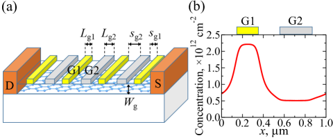
Figure 1(a) shows a dual-grating-gate graphene FET under consideration. In our simulation model, we assume that the number of periods of the grating gates is sufficiently large, i.e., the total channel length is longer than the THz/mid-infrared wavelength, so that we can ignore effects of nonperiodicity such as the presence of the source and drain contacts and we can consider one period as a unit cell. We fix the thickness of the gate dielectric, nm, the left spacings of the gates 1 and 2, nm, nm, whereas we vary the lengths of the gate 1 and 2, and , in the range between and nm in order to reveal characteristics of the instabilities obtained in this work by comparison with existing theory. The values of those parameters were chosen such a way that frequencies of self-excited plasmons fall into the THz/mid-infrared range. The dielectric constant of media surrounding the graphene channel is set to . Figure 1(b) is a profile of the steady-state electron concentration without current flow, and it was calculated self-consistently with a uniform electron doping cm-2 together with certain gate voltages. The slight electron doping is introduced to avoid plasmon damping due to the electron-hole friction Svintsov et al. (2012); even at the point with the lowest electron concentration, the hole concentration is negligibly low, cm-2. On the other hand, the highest electron concentration is set not so high that the difference between maximum and minimum Fermi energies ( and meV, respectively) does not exceed optical-phonon energies in graphene and thus electrons injected quasi-ballistically from the region with high electron concentration do not experience optical-phonon emission, which would critically hinder the RSS instability.
We use the quasi-classical Boltzmann equation to describe the electron transport in the channel:
| (1) |
where cm/s is the Fermi velocity in graphene, is the self-consistent electric field in graphene, and is the momentum. In the right-hand side of Eq. (1), we take into account collision integrals for the acoustic-phonon scattering, , where
| (2) |
and an explicit expression of the transition probability can be found in Ref. Hwang and Das Sarma (2008). We use the so-called weighted essentially nonoscillatory finite-difference scheme Carrillo et al. (2003); Galler and Schürrer (2006) to solve Eq. (1), which is demonstrated to be applicable for graphene transport simulation Lichtenberger et al. (2011). The time-step of the simulation was set to fs to avoid numerical instabilities. The 2D Poisson equation is solved self-consistently with Eq. (1) using a finite-element library called libMesh Kirk et al. (2006). Periodic boundary conditions are set for both the potential and electron distribution function. More detail of the simulation model is described elsewhere Satou et al. (2013).
A simulation starts by applying a uniform external dc electric field in the channel direction, , to inject positive source-drain dc current. To avoid unwanted plasmon excitation associated with an abrupt turn-on of the dc electric field, an artificially large damping factor is set in front of the collision integral in Eq. (1), and it is gradually decreased to unity within 6 picoseconds, which is much longer than the inverse of plasmon frequency obtained in the simulation. Then, the electron concentration, electric field, etc. begin to oscillate and their amplitudes increase with time as shown in Fig. 2(a). This is identified as occurence of plasmon instability.
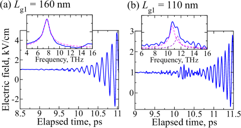
In general, oscillations simulated contain several modes. With certain sets of parameters distinct fundamental modes can be obtained, and the frequency and total growth rate can be easily extracted. However, with other sets they contain fundamental and second modes with very close frequencies and/or higher harmonics which have comparable amplitudes with the fundamental modes, resulting in the beating (see Fig. 2(b)) and/or the distortion of waveforms. To extract the frequency and total growth rate of the fundamental mode, we perform the Fourier transform of the oscillation with respect to time, pick up the first peak and another close peak, if any, and perform a curve fitting to them with the following function:
| (3) |
Equation (3) is equal to the absolute value of the Fourier transform of the summation of two exponentially growing harmonic functions around its peak(s). As seen in the insets of Figs. 2(a) and (b), The fundamental and adjacent second modes can be well separated by this method.
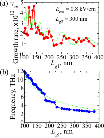
Figures 3(a) and (b) show the total growth rate and frequency of the fundamental mode as a function of the length of the gate 1 with kV/cm and with nm. They clearly demonstrates the total growth rate of the instability exceeding s-1 with the frequency in the THz/mid-infrared range. This value is an order of magnitude larger than achievable in FETs or HEMTs based on usual semiconductors at room temperature. This giant total growth rate of the plasmon instability in the dual-grating-gate graphene FET is attributed to the lower plasmon damping and also to the larger drift velocity, both originating from the lower scattering rate limited only by acoustic phonons. This point shall be discussed in more detail shortly later.
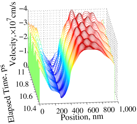
The gate-length dependence of the total growth rate exhibits an oscillatory behavior; the oscillation period becomes shorter and the amplitude becomes larger as the gate length becomes shorter. It is specific to the RSS instability, and it corresponds to the constructive/destructive interference between plasmons in the high-concentration region (under the gate 1) and the bunched electrons in the low-concentration region (under the gate 2). This effect is illustrated in Fig. 4 where an oscillation of the electron velocity is built up at the left edge of the high-concentration region (near nm), where the electrons are injected to the low-concentration region. Besides, there is a monotonically increasing portion of the total growth rate with decreasing in Fig. 3(a). This can be attributed to the DS instability, in which the growth rate is inversely porportional to the traveling time of plasmons in the gated region and therefore, to the gate length Dyakonov and Shur (1993). Those characteristics signify the simultaneous occurence of the DS and RSS instabilities. In fact, the overall characteristics of the growth rate can be described qualitatively well by the formula according to Ref. Ryzhii et al. (2006), which is a linear superposition of the growth rates of those instabilities:
| (4) |
where cm/s, cm/s, and nm are fitting parameters (see the fitting curve in Fig. 3(a)).
As seen in Fig. 3(b), the frequency is almost inversely proportional to , and it obeys the well-known dispersion of gated 2D plasmons,
| (5) |
where cm/s is the plasmon phase velocity which is extracted as a fitting parameter and which is quantitatively consistent with the value calculated analytically Ryzhii (2006) for the region under the gate 1.
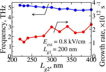
The giant instability found here at room temperature originates from the ultimately weak electron scattering rate in graphene, and there are two factors for this: (1) the weak damping of plasmons and (2) the large drift velocity in both high- and low-concentration regions that leads to large DS and RSS instabilities, respectively. First, the estimated damping rate was around s-1 in the low-concentration region and s-1 in the high-concentration region; note that the electron scattering rate, and thus the plasmon damping rate, for the acoustic-phonon scattering is proportional to the square root of the electron concentration Hwang and Das Sarma (2008); Satou et al. (2013). Such low values of the plasmon damping rate can be achieved only at nitrogen temperature or lower in other materials. It is worth mentioning that the low-concentration region with adjacent ungated regions acts as a better (passive) plasmon resonant cavity, while the instabilities take place primarily for plasmons in the high-concentration region, as is evident from the dependence of the frequency on and its consistency with Eq. (5), and the frequency is insensitve to the length of the gate 2 as shown in Fig. 5 (in contrast, the total growth rate can vary with it). This is similar to the situation discussed in Ref. Popov et al. (2008b), where the ungated plasmon resonance can be effectively tuned by the gated region of the channel. In fact, it can be seen in Fig. 4 that a higher harmonic oscillation with more than one nodes is excited in the low-concentration region. This together with the oscillation in the high-concentration region form the fundamental mode of the whole period.
In addition, values of drift velocities obtained in the simulation, cm/s in the low-concentration region and cm/s in the high-concentration region, confirm the factor (2) for the giant growth rate. Especially the former is more than twice larger than the saturation velocity in Si and InGaAs channels. However, the velocities extracted by Eq. (4) as fitting parameters differ from these values by several factors. A reasonable explanation to this discrepancy is that the DS instability also takes place not only in the high-concentration region but also in the low-concentration region. Fig. 4 exhibits waves propagating in opposite directions in the latter, suggesting the occurence of the DS instability there. This should add a constant term in Eq. (4), and then the fitting velocities should become closer to the simulated values.
In conclusion, we have conducted simulations of plasmon instability driven by dc current injection in the dual-grating-gate graphene FET. We have obtained a giant total growth rate of the instability at room temperature exceeding s-1. Through the dependences of the total growth rate and frequency on the gate lengths, we have revealed that the giant total growth rate originates from simulateneous occurence of the DS and RSS instabilities. The result obtained strongly suggests that a graphene FET with the dual-grating-gate structure is very promising for the realization of a high-power, compact, room-temperature operating THz source.
This work was financially supported by JSPS Grant-in-Aid for Young Researcher (#26820122), by JSPS Grant-in-Aid for Specially Promoted Research (#23000008), and by JSPS and RFBR under Japan-Russia Research Cooperative Program. The simulation was carried out using the computational resources provided by Research Institute for Information Technology Center, Nagoya University, through the HPCI System Research Project (#hp140086), by the Information Technology Center, the University of Tokyo, and by Research Institute for Information Technology, Kyushu University.
References
- Allen et al. (1977) S. J. Allen, D. C. Tsui, and R. A. Logan, Phys. Rev. Lett. 38, 980 (1977).
- Dyakonov and Shur (1993) M. Dyakonov and M. Shur, Phys. Rev. Lett. 71, 2465 (1993).
- Dyakonov and Shur (1996) M. Dyakonov and M. Shur, IEEE Trans. Electron Devices 43, 380 (1996).
- Veksler et al. (2006) D. Veksler, F. Teppe, A. P. Dmitriev, V. Y. Kachorovskii, W. Knap, and M. S. Shur, Phys. Rev. B 73, 125328 1 (2006).
- Dyer et al. (2013) G. C. Dyer, G. R. Aizin, S. J. Allen, A. D. Grine, D. Bethke, J. L. Reno, and E. A. Shaner, Nature Photonics 7, 925 (2013).
- Rozhansky et al. (2015) I. V. Rozhansky, V. Y. Kachorovskii, and M. S. Shur, Phys. Rev. Lett. 114, 246601 (2015).
- Shur and Ryzhii (2003) M. S. Shur and V. Ryzhii, Int. J. High Speed Electron. Syst. 13, 575 (2003).
- Knap et al. (2009) W. Knap, M. Dyakonov, D. Coquillat, F. Teppe, N. Dyakonova, J. Łusakowski, K. Karpierz, M. Sakowicz, G. Valusis, D. Seliuta, I. Kasalynas, A. Fatimy, Y. M. Meziani, and T. Otsuji, J. Infrared, Millim., and THz Waves 30, 1319 (2009).
- Otsuji and Shur (2014) T. Otsuji and M. Shur, IEEE Microw. Mag. 15, 43 (2014).
- Otsuji (2015) T. Otsuji, IEEE Trans. THz Sci. Tech. 5, 1110 (2015).
- Dmitriev et al. (1997) A. P. Dmitriev, A. S. Furman, V. Y. Kachorovskii, G. G. Samsonidze, and G. G. Samsonidze, Phys. Rev. B 55, 10319 (1997).
- Dyakonov and Shur (2005) M. Dyakonov and M. S. Shur, Appl. Phys. Lett. 87, 111501 (2005).
- Popov et al. (2008a) V. V. Popov, G. M. Tsymbalov, and M. S. Shur, J. Phys.: Condens. Matter 20, 384208 (2008a).
- Ryzhii et al. (2005) V. Ryzhii, A. Satou, and M. S. Shur, Phys. Stat. Sol. (A) 202, 113 (2005).
- Ryzhii et al. (2006) V. Ryzhii, A. Satou, and M. S. Shur, IEICE Trans. on Electron. E89-C, 1012 (2006).
- Ryzhii et al. (2008) V. Ryzhii, A. Satou, M. Ryzhii, T. Otsuji, and M. S. Shur, J. Phys.: Condens. Matter 20, 384207 (2008).
- Otsuji et al. (2006) T. Otsuji, M. Hanabe, T. Nishimura, and E. Sano, Opt. Exp. 14, 4815 (2006).
- Popov et al. (2011) V. V. Popov, D. V. Fateev, T. Otsuji, Y. M. Meziani, D. Coquillat, and W. Knap, Appl. Phys. Lett. 99, 243504 (2011).
- Otsuji et al. (2008) T. Otsuji, Y. M. Meziani, T. Nishimura, T. Suemitsu, W. Knap, E. Sano, T. Asano, and V. V. Popov, J. Phys.: Condens. Matter 20, 384206 (2008).
- Ryzhii (2006) V. Ryzhii, Jpn. J. Appl. Phys. 45, L923 (2006).
- Ryzhii et al. (2007) V. Ryzhii, A. Satou, and T. Otsuji, J. Appl. Phys. 101, 24509 (2007).
- Mikhailov (2011) S. A. Mikhailov, Phys. Rev. B 84, 045432 (2011).
- Dubinov et al. (2011) A. A. Dubinov, V. Y. Aleshkin, V. Mitin, T. Otsuji, and V. Ryzhii, J. Phys. Cond. Matt. 23, 145302 (2011).
- Ju et al. (2011) L. Ju, B. Geng, J. Horng, C. Girit, M. Martin, Z. Hao, H. a. Bechtel, X. Liang, A. Zettl, Y. R. Shen, and F. Wang, Nature Nanotech. 6, 630 (2011).
- Vicarelli et al. (2012) L. Vicarelli, M. S. Vitiello, D. Coquillat, A. Lombardo, A. C. Ferrari, W. Knap, M. Polini, V. Pellegrini, and A. Tredicucci, Nature Materials 11, 865 (2012).
- Wang et al. (2012) B. Wang, X. Zhang, F. J. García-Vidal, X. Yuan, and J. Teng, Phys. Rev. Lett. 109, 073901 (2012).
- Svintsov et al. (2012) D. Svintsov, V. Vyurkov, S. Yurchenko, T. Otsuji, and V. Ryzhii, J. Appl. Phys. 111, 083715 (2012).
- Grigorenko et al. (2012) A. N. Grigorenko, M. Polini, and K. S. Novoselov, Nature Photonics 6, 749 (2012).
- Popov et al. (2013) V. V. Popov, O. V. Polischuk, S. A. Nikitov, V. Ryzhii, T. Otsuji, and M. S. Shur, J. Opt. 15, 114009 (2013).
- Hwang and Das Sarma (2008) E. H. Hwang and S. Das Sarma, Phys. Rev. B 77, 115449 (2008).
- Satou et al. (2013) A. Satou, V. Ryzhii, F. T. Vasko, V. V. Mitin, and T. Otsuji, Proc. SPIE 8624, 862412 (2013).
- Wang et al. (2013) L. Wang, I. Meric, P. Y. Huang, Q. Gao, Y. Gao, H. Tran, T. Taniguchi, K. Watanabe, L. M. Campos, D. a. Muller, J. Guo, P. Kim, J. Hone, K. L. Shepard, and C. R. Dean, Science 342, 614 (2013).
- Carrillo et al. (2003) J. A. Carrillo, I. M. Gamba, A. Majorana, and C.-w. Shu, J. Comp. Phys. 184, 498 (2003).
- Galler and Schürrer (2006) M. Galler and F. Schürrer, J. Comp. Phys. 212, 778 (2006).
- Lichtenberger et al. (2011) P. Lichtenberger, O. Morandi, and F. Schürrer, Phys. Rev. B 84, 045406 (2011).
- Kirk et al. (2006) B. S. Kirk, J. W. Peterson, R. H. Stogner, and G. F. Carey, Eng. Comp. 22, 237 (2006).
- Popov et al. (2008b) V. V. Popov, A. N. Koudymov, M. Shur, and O. V. Polischuk, J. Appl. Phys. 104, 024508 (2008b).