Spilling of electronic states in Pb Quantum Wells
Abstract
Energy-dependent apparent step heights of two-dimensional ultra-thin Pb islands grown on the Si(111)66Au surface have been investigated by a combination of scanning tunneling microscopy, first-principles density functional theory and the particle in a box model calculations. The apparent step height shows the thickness and energy dependent oscillatory behavior, which is directly related to the spilling of electron states into the vacuum exhibiting a quantum size effect. This has been unambiguously proven by extensive first-principles scanning tunneling microscopy and spectroscopy simulations. An electronic contribution to the apparent step height is directly determined. At certain energies it reaches values as high as a half of the atomic contribution. The applicability of the particle in a box model to the spilling of electron states is also discussed.
pacs:
68.65.Fg, 73.21.Fg, 68.37.EfI Introduction
Behavior of metallic quantum wells (QW) on semiconductor surfaces exhibiting quantum-size effects (QSE) has been a topic of great fundamental interest for many years Chiang (2000); Jia et al. (2007); Vázquez de Parga et al. (2009). The spatial confinement of electrons and the presence of discrete electronic subbands affect electronic properties of ultrathin films, as shown for the electrical resistivity Jałochowski and Bauer (1988); Jałochowski et al. (1992a, 1995), Hall coefficient Jałochowski et al. (1996); Vilfan et al. (2002), surface morphology Altfeder et al. (1997); Su et al. (2001); Otero et al. (2002); Jian et al. (2003); Unal et al. (2007); Binz et al. (2008); Kopciuszyński et al. (2015), surface energy Materzanini et al. (2001); Wei and Chou (2002), work function Qi et al. (2007); Becker and Berndt (2010), chemical reactivity Jiang et al. (2008), electron phonon coupling Zhang et al. (2005), superconducting transition temperature Guo et al. (2004); Brun et al. (2009), Kondo temperature Fu et al. (2007), Rashba spin-orbit interaction Slomski et al. (2011), and Friedel oscillations Jia et al. (2010); Bouhassoune et al. (2014), to name a few.
Ultrathin Pb layers have been a prominent test laboratory for studying electronic quantum effects in nanoscale metallic objects. Theoretical and experimental studies indicated that structural and morphological properties of ultrathin Pb films are related to QSE. Minimization of the total internal energy of Pb island with a thickness dependent QSE electronic component leads to the growth of islands with preferential magic thicknesses Budde et al. (2000); Yeh et al. (2000); Su et al. (2001); Hupalo et al. (2001); Hupalo and Tringides (2002); Otero et al. (2002); Binz et al. (2008). In a continuous layer this minimization manifests itself as a variation of the measured Pb apparent step height (ASH). Expansion and contraction of the top layer were observed in the scattering of He atoms from Pb epitaxial layers on Cu(111) Braun and Toennies (1997) and on Ge(001) Crottini et al. (1997) substrates. The density functional theory (DFT) calculations confirmed QSE origin of the 2 ML periodicity in the expansion/contraction of Pb layers separation Materzanini et al. (2001). The apparent step height has also been measured by x-ray diffraction Czoschke et al. (2003) and scanning tunneling microscopy (STM) in a number of QSE systems Su et al. (2001); Hupalo et al. (2001); Otero et al. (2002); Unal et al. (2007); Vázquez de Parga et al. (2009); Calleja et al. (2009).
It has been proposed that the main reason for oscillation of the ASH is a thickness-dependent variation of an electron density outside the quantized film. Moreover, it was found that the ASH may depend on the energy, or on the STM bias, chosen to probe the sample, since the quantum well state (QWS) dominates the electronic structure of the system Vázquez de Parga et al. (2009). In the simplest approach, i.e. within a free-electron model applied to a finite quantum well, the states ”spill out” of the geometrical border of the well Schulte (1976). The spilling should be larger for the QWSs closer to the vacuum level. Thus, it can be expected that the measured thickness of the QW depends on the energy of sampling electrons. The STM technique is exceptionally well suited to study such effects. In particular, the STM enables the exploration of surface electron densities within a broad energy range around the Fermi level.
In the present work we address the issue of bias-dependence of the apparent step height in quantum wells, and unambiguously prove that the spilling of electron states into the vacuum is governed by energy position of QWS. We determine the electronic contribution to the ASH, which is a substantial fraction of the atomic contribution, and at certain energies it may reach value as high as a half of that coming from the atoms arrangement. We prove that the electronic effects prevail the atomic lattice expansion/contraction, the electronic effects may even overwhelm the atomic ones leading to reversing of the apparent step height variation upon change of the sample bias in the STM experiments. As an example, we consider Pb quantum wells on Si(111)66-Au substrate. This substrate was chosen because of the specific Pb growth mode achievable Schmidt and Bauer (2000). Even the first monatomic layer of Pb film has well defined crystalline structure and exhibits clear QSE Jałochowski et al. (1992b). The STM topography measurements reveal the thickness- and bias-dependence of the apparent step height. A direct relation between the ASH and the spilling of QWSs into the vacuum is unambiguously proven by extensive first-principles scanning tunneling microscopy simulations based on DFT. Depending on energy the QWS can evanesce in the vacuum at different distances. The above observations are explained semi-qualitatively within the particle in a box model, which confirms the applicability of this model to QSE systems. The present study shows that in ultrathin metallic films step height determination with STM has to be accompanied by at least simple analysis based on finite quantum well model of the QSE states, and their contribution to the bias dependent tunneling current.
II Experimental and computational details
Samples were prepared in an ultra-high vacuum (UHV) chamber equipped with a STM (type OMICRON VT) and reflection high energy electron diffraction (RHEED) apparatus. The base pressure was mbar. In order to produce Si(111)66-Au reconstruction about 1.6 ML of Au was deposited onto the Si(111)77 substrate and annealed for 1 min. at about 950 K, and then the temperature was gradually lowered to about 500 K within 3 min. Direct resistive heating was used. A series of the Pb films with average thickness between 0.5 to 6 ML have been in situ deposited onto the substrate held at 170 K in the STM stage. The deposition rate was equal to 0.2 ML of Pb(111) per minute. All STM measurements were performed at the sample temperature equal to 170 K and the tunneling current equal to 0.1 nA.
Density functional theory calculations were performed within Perdew-Burke-Ernzerhof (PBE) Perdew et al. (1996) generalized gradient approximation (GGA) using projector-augmented-wave potentials, as implemented in VASP (Vienna ab-initio simulation package) Kresse and Furthmüller (1996); Kresse and Joubert (1999). The plane wave energy cutoff for all calculations was set to 340 eV, and the Brillouin zone was sampled by a Monkhorst-Pack k-points grid Monkhorst and Pack (1976). The spin-orbit interaction was omitted.
To simplify calculations, the Si(111)-Au unit cell has been adapted, which is locally similar to the Si(111)66-Au Jałochowski (2003). The Si(111)-Au system has been modeled by 8 Si double layers and the reconstruction layer. A vacuum region of 20 Å has been added to avoid the interaction between surfaces of the slab. All the atomic positions were relaxed, except the bottom layer, until the largest force in any direction was below 0.01 eV/Å. The Si atoms in the bottom layer were fixed at their ideal bulk positions and saturated with hydrogen. The lattice constant of Si was fixed at the calculated value, 5.47 Å.
Based on the obtained electronic structure data of the Si(111)-Au surface described above, scanning tunneling microscopy simulations were performed by using Bardeen’s electron tunneling model Bardeen (1961) implemented in the BSKAN code Hofer (2003); Palotás and Hofer (2005); Hofer and Garcia-Lekue (2005). The employed tunneling model takes into account electronic structures of both the Si(111)-Au surface and tungsten tips. We considered blunt and sharp tungsten tip models following Refs. Teobaldi et al. (2012); Mándi et al. (2015) to investigate the effect of tip sharpness on the apparent step height. The blunt tip is represented by an adatom adsorbed on the hollow site of the W(110) surface, and the sharp tip is modeled as a pyramid of three-atoms height on the W(110) surface. More details on the used tip geometries and electronic structure calculations can be found in Ref. Teobaldi et al. (2012). Note that the shape of the tip apex structure will influence the transmission probability via the Bardeen tunneling matrix elements, thus the tunneling current.
III Results and discussion
For coverages studied here Pb formed well resolved 1 and/or 2 ML thick islands. Their average lateral size increased with the average film thickness. For average coverages less than 1 ML, Fig. 1 (a), only 1 ML thick islands and single Pb atoms were seen.
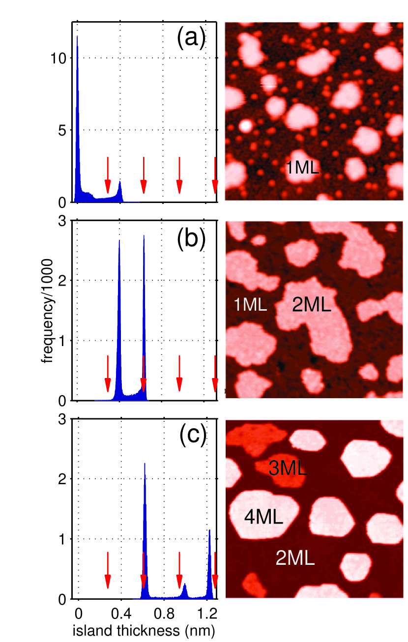
After deposition of 1 ML Pb the surface of the film was flat. For average coverages between 1 and 2 ML, Fig. 1 (b), only 1 ML high islands on the 1 ML thick Pb background were seen. No islands were seen after deposition of 2 ML. Further increase of the coverage, within the range from 2 to 4 ML, resulted in the growth of a mixture of 1 and 2 ML thick islands, as shown in Fig. 1 (c). At the coverage equal to 4 ML the film was again perfectly flat. This process was repeated for the coverages between 4 and 6 ML of Pb. Thus, at this particular temperature of deposition, the film grew in a layer by layer mode for the coverages up to 2 ML and in the mixed single and double monolayer modes for the larger coverages. Apparently, the 2, 4, and 6 ML thick films are more stable than those with an odd number of monolayers. This finding agrees well with the theoretical predictions Materzanini et al. (2001).
The apparent step height was determined from STM topographic data similar to that presented in Fig. 1. A large number of the samples with various coverages was produced and scanned with a sample bias Vbias ranging from -2.5 V to +2.0 V. Next, the inevitable slope of the image background was carefully corrected and the image height histograms were calculated. The presence of the Si(111) steps (not shown here) allowed the calibration of the STM vertical gain. Examples of the histograms are shown in Fig. 1. Series of STM scans, similar to that displayed in Fig. 1, produced plots of the ASHs as a function of the sample bias. Figure 2 (a) shows the averaged data of several samples.
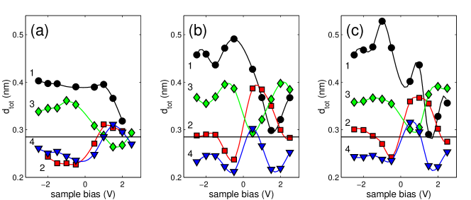
The accuracy of the ASH determination was estimated to be 0.01 nm. Two interesting features are seen. First, all curves show strong bias dependence. Second, the ASHs on the film with odd number of monolayers behave opposite to those on even number of monolayers (including the 1 ML on the substrate). For negatively biased samples the ASH of 2 ML and 4 ML Pb, the measured apparent step height is much lower than the bulk value nm, whereas for 1 ML and 3 ML Pb, it is noticeably larger. As a consequence, for a fixed bias, especially for the negative bias, the ASH varies with 2 ML periodicity.
In order to explain the observed oscillations of the ASH we have performed extensive first-principles STM simulations based on DFT. First, the STM topography images of the surfaces consisting of a different number of Pb layers have been calculated in the constant current mode for various voltages and the tunneling current, corresponding to the experimental value. Next, to get the ASH of the -th layer, we averaged the topography of the surface with layers over the surface unit cell, and subtracted the corresponding value for the surface with layers. Such procedure is closely related to the experimentally determined ASH, and the results of calculations with the model blunt and sharp tips are shown in Fig. 2 (b) and (c), respectively. The two tip models give similar results for the trends of the ASH, thus we can conclude that the bias voltage dependent ASH is governed by the QW states of the surface. This also suggests that the possible instability of the tip in STM experiments is not expected to qualitatively alter the measured ASH, which might turn out to be very useful for future experimental STM studies of QWS. Clearly, the experimental data of Fig. 2 (a) are reproduced well, especially for negative sample bias. A poorer agreement in the empty state regime is due to known limitations of DFT approach. Note however, that the empty-state DFT results coincide with the experimental data, provided they are artifically shifted by V (compare panels (a) and (b) of Fig. 2). Perhaps more sophisticated approaches, like GW or time-dependent DFT, should give better agreement in the empty state regime. Slightly higher values calculated for 1 ML Pb, than the experimentally found are due to different substrates used in the experiment and in calculations, as it was discussed in Sec. II. Nevertheless, the shape of the calculated 1 ML ASH is very similar to the experimental one.
Strong dependence of the apparent step height on the tunneling bias suggests the electronic origin of the observed phenomena. The procedure used in calculations allows to directly determine both the atomic as well as the electronic contributions to ASH. In general, the ASH, , can be expressed as
| (1) |
where is the atomic contribution, simply given by difference of the z-coordinates of the atoms forming 2 subsequent layers of Pb, and independent of the sample bias. is the height associated with the electronic contribution to the ASH, obviously bias dependent. The atomic and electronic contributions to the ASH as a function of the Pb layer number are shown in Fig. 3.
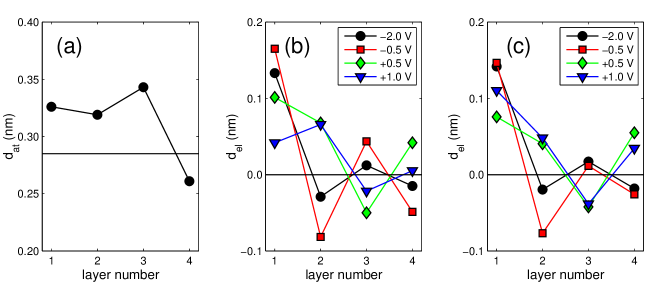
The atomic contribution is the same for both considered tip models [Fig. 3 (a)], whereas the electronic contributions are shown in Fig. 3 (b) and (c), respectively calculated using the blunt and sharp tip models. Similarly to Fig. 2, we find that the two geometrically different tip apex structures provide similar trends for the electronic contribution of the ASH. Moreover, it is seen that all parts of Fig. 3 oscillate with periodicity of 2 ML Pb, and the electronic contribution can be positive or negative.
Interestingly, the electronic part features higher amplitude of the oscillations, than the atomic part. This amplitude depends on the sample bias, and increases as the absolute value of sample bias is decreased. As a result, at certain bias voltages, the electronic contribution to the ASH may be as large as a half of the atomic one, especially for thinner Pb QWs. Compare the -0.5 V curve in panel (b) with panel (a). All this confirms that the ASH measured by STM is substantially influenced by the electronic effects, i.e. by the spilling of the quantum well states into the vacuum.
To get a deeper and more intuitive insight into the spilling of the QWS and its impact on the apparent step height, we evoke the one-dimensional model of a noninteracting electron gas confined in a finite square QW. Albeit this model neglects the layered crystal structure of the film and the presence of the substrate, it was previously successfully applied in explanation of the QSE in the electron photoemission Jałochowski et al. (1992b). The simple 1D QW model focuses on basic physics related to the ASH effects observed in real experiment. In this model width of the quantum well is equal to , with being the number of the Pb monolayers, the effective electron mass is equal to , the Fermi energy is equal to eV, and the work function is equal to eV. For each QW the shape of the wavefunctions and their energy were calculated. For explanation of the measured variation of the ASH the interesting quantity is the expansion (spilling out) of the wavefunctions outside of the film and its dependence on energy of the quantum state.
Figure 4 (a) shows the energies of the QW states and corresponding wavefunctions for a QW of the width of 2 ML Pb.
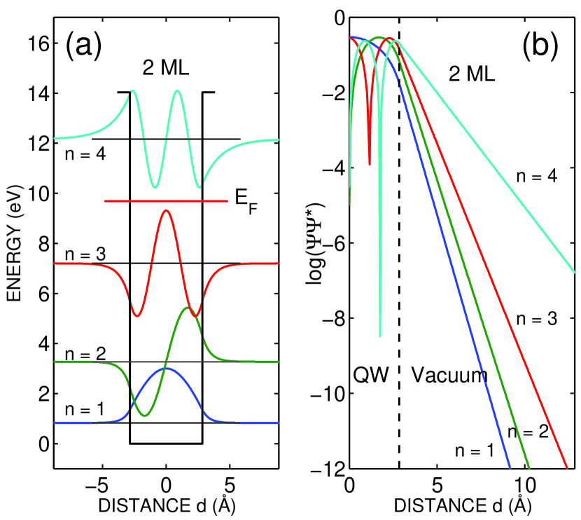
Note the spilling out of the wavefunctions outside the well. As it is displayed in Fig. 4 (b) in the logarithmic scale, outside the QW the density of states of decays exponentially with the slope of depending on the energy of the quantum level. To understand the physical origin of the apparent step height oscillation and its bias dependence, we recall the Tersoff-Hamann Tersoff and Hamann (1983) approach to the tunneling. The Tersoff-Hamann model can be derived from the Bardeen tunneling formula by assuming an s-type tip. This popular model, though very simple, works reasonably well to understand electron tunneling and STM images in a large variety of surface systems with simple electronic structure. To provide a simple physical picture for the understanding of the ASH oscillations involving the QW states in our 1D QW model, we have used the Tersoff-Hamann tunneling model assuming that the transmission probability through the barrier and density of states of the tip are constant at all energies. This is sufficient to capture the basic physics in QW systems. According to the Tersoff-Hamann model, the tunneling current is described by the equation:
| (2) |
Here denotes the local density of the state at the tip position R. In the case of extremely thin QW studied here, and the bias ranges applied, only single highest occupied (HO) or the lowest unoccupied (LU) QW states contribute to the tunneling current at once. The Eq. 2 shows that the tunneling current is proportional to the local density of states at the position of STM tip, the quantity displayed in the Fig. 4 (b). Correspondingly, the condition of constant tunneling current to, or from one specific QW level, requires adjusting the tip at the distance where is the same. Consequently, the tunneling condition was set as typical, with experimental sample-tip distance equal 5 Å Seine et al. (1999). From the figure 4(b) follows that such distance, at least for states n = 3 and 4, i.e. states located within the energy range used in the experiment, corresponds to the electron density between and . Therefore we have chosen the logarithmic mean value of in calculations. Figure 5 shows both, the calculated energies of the LU and HO states [panel (a)], and the distances at which their density is equal to [panel (b)].
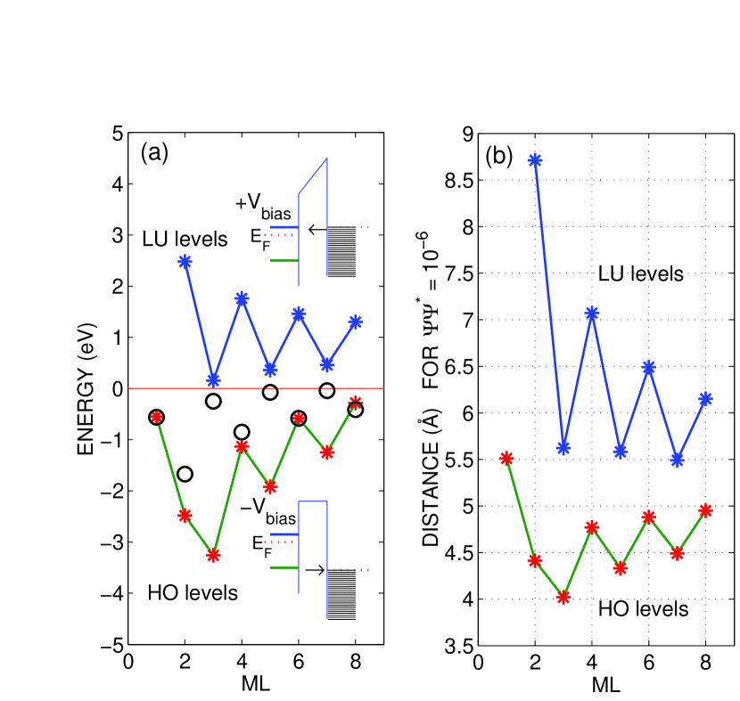
It is worthwhile to note that experimentally determined positions of the QW states Jałochowski et al. (1992b) shown in the Fig. 5 (a) as open circles, lie close to the theoretical ones and show similar thickness dependence. Based on the data of the Fig. 5 (b) the origin of the bias dependence of the apparent step height shown in Fig. 2, can be explained as follows.
1 ML Pb. Here only one quantum state is accessible for tunneling. According to the data of Fig. 5 (a) it lies about 0.5 eV below the and the tunneling current can flow easily for negatively biased sample. This state spills far into vacuum and its energy position is almost independent of vector. Moreover, it spreads over a large part of the Brillouin zone. For these reasons, the tunneling current is high and the STM tip has to be retracted, giving large value of the ASH at negative sample bias. For the positively biased sample there is no accessible state and in order to keep the same tunneling current, the tip has to be moved closely to the sample. As the curve 1 in Fig. 2 (a) shows, the measured ASH changes from 0.4 nm to about 0.32 nm, for -2 V and +2 V of the sample bias, respectively.
2 ML Pb. For this QW two quantum states can contribute to the tunneling current. Both the HO and the LU states are placed approximately symmetrically to the Fermi energy, but their spilling differs considerably, compare QW states n = 3 and 4 in Fig. 4 (a) and (b). For n = 4 state (LU) the charge density is obtained at the distance around 4 Å larger than in the case of n =3 state (HO). Consequently, the STM tip has to be retracted for positive sample bias. Exactly this behavior is observed in Fig. 2 for curves with , albeit the ASH yields Å.
3 ML Pb. The behavior of the bias-dependent ASH resembles the situation in the case of a single Pb layer on the bare substrate (), as the HO state is located below the Fermi energy. However its energy is almost 3 eV lower than in the case of . Thus, such low energy should not contribute to the current in the bias range used in the experiment. However, this state is more dispersive, and the tunneling to the at lower voltages dominates. Moreover, the photoemission-determined QW state for 3 ML thick QW Jałochowski et al. (1992b) is located just below the Fermi energy. Note, that according to the model calculation, this state is located above, albeit very close to the EF. In real situation, we can assume that this state will contribute to current at both sample bias polarizations. Thus the difference in the ASH for positive and negative sample bias is expected to be smaller, as comapred to the case. Indeed this can be seen in Fig. 2 (curve 3).
4 ML Pb. The situation reverses again and resembles the case of . The HO and LU states are located approximately symmetrically with respect to the EF at energies, which are captured by present STM measurements. Moreover, the LU state extends much further into vacuum than the HO, see Fig. 5 (b), thus the observed ASH is higher at the positive sample bias, as it is shown in Fig. 2 (curve 4).
The above discussion clearly indicates that this simple model explains the most important features of the experimental data and of the DFT calculations such as variation of the apparent step height with the sample bias and its oscillations with 2 ML periodicity.
IV Conclusions
In conclusion, the apparent step height measured by scanning tunneling microscopy shows the thickness and energy dependent oscillatory behavior, which is directly related to the spilling of quantum well states into the vacuum. The electronic contribution to the apparent step height can be as large as a half of that coming from the arrangement of atoms. Thus the interpretation of step height in ultrathin film determined with scanning tunneling microscopy needs a great care and knowledge of its energy dependence. Finally, the simple model of the particle in a box contains most of the relevant physics to be successfully applied for systems exhibiting quantum size effect.
Acknowledgements.
The work has been supported by the National Science Centre (Poland) under Grant No. DEC-2014/13/B/ST5/04442. K.P. acknowledges the Hungarian State Eötvös Fellowship and the EU COST MP1306 EUSPEC project.References
- Chiang (2000) T.-C. Chiang, Surf. Sci. Rep. 39, 181 (2000).
- Jia et al. (2007) J.-F. Jia, S.-C. Li, Y.-F. Zhang, and Q.-K. Xue, J. Phys. Soc. Jpn. 76, 2007 (2007).
- Vázquez de Parga et al. (2009) A. L. Vázquez de Parga, J. J. Hinarejos, F. Calleja, J. Camarero, R. Otero, and R. Miranda, Surf. Sci. 603, 1389 (2009).
- Jałochowski and Bauer (1988) M. Jałochowski and E. Bauer, Phys. Rev. B 38, 5272 (1988).
- Jałochowski et al. (1992a) M. Jałochowski, H. Knoppe, G. Lilienkamp, and E. Bauer, Phys. Rev. B 46, 4693 (1992a).
- Jałochowski et al. (1995) M. Jałochowski, M. Hoffmann, and E. Bauer, Phys. Rev. B 51, 7231 (1995).
- Jałochowski et al. (1996) M. Jałochowski, M. Hoffmann, and E. Bauer, Phys. Rev. Lett. 76, 4227 (1996).
- Vilfan et al. (2002) I. Vilfan, M. Henzler, O. Pfennigstorf, and H. Pfnur, Phys. Rev. B 66, 241306 (2002).
- Altfeder et al. (1997) I. Altfeder, K. Matveev, and D. Chen, Phys. Rev. Lett. 78, 2815 (1997).
- Su et al. (2001) W. Su, S. Chang, W. Jian, C. Chang, L. Chen, and T. Tsong, Phys. Rev. Lett. 86, 5116 (2001).
- Otero et al. (2002) R. Otero, A. L. Vázquez de Parga, and R. Miranda, Phys. Rev. B 66, 115401 (2002).
- Jian et al. (2003) W. Jian, W. Su, C. Chang, and T. Tsong, Phys. Rev. Lett. 90, 196603 (2003).
- Unal et al. (2007) B. Unal, F. Gin, Y. Han, D.-J. Liu, D. Jing, A. R. Layson, C. J. Jenks, J. W. Evans, and P. A. Thiel, Phys. Rev. B 76, 195410 (2007).
- Binz et al. (2008) S. M. Binz, M. Hupalo, and M. C. Tringides, Phys. Rev. B 78, 193407 (2008).
- Kopciuszyński et al. (2015) M. Kopciuszyński, P. Dyniec, M. Krawiec, M. Jałochowski, and R. Zdyb, Appl. Surf. Sci. 331, 512 (2015).
- Materzanini et al. (2001) G. Materzanini, P. Saalfrank, and P. Lindan, Phys. Rev. B 63, 235405 (2001).
- Wei and Chou (2002) C. Wei and M. Chou, Phys. Rev. B 66, 233408 (2002).
- Qi et al. (2007) Y. Qi, X. Ma, P. Jiang, S. Ji, Y. Fu, J. Jia, Q. Xue, and S. Zhang, Appl. Phys. Lett. 90, 013109 (2007).
- Becker and Berndt (2010) M. Becker and R. Berndt, Appl. Phys. Lett. 96, 033112 (2010).
- Jiang et al. (2008) P. Jiang, X. Ma, Y. Ning, C. Song, X. Chen, J.-F. Jia, and Q.-K. Xue, J. Am. Chem. Soc. 130, 7790 (2008).
- Zhang et al. (2005) Y. Zhang, J. Jia, T. Han, Z. Tang, Q. Shen, Y. Guo, Z. Qiu, and Q. Xue, Phys. Rev. Lett. 95, 096802 (2005).
- Guo et al. (2004) Y. Guo, Y.-F. Zhang, X.-Y. Bao, T.-Z. Han, Z. Tang, Z.-X. Zhang, W.-G. Zhu, E. Wang, Q. Niu, Z. Qiu, et al., Science 306, 1915 (2004).
- Brun et al. (2009) C. Brun, I. Hong, F. Pattney, I. Sklyadneva, R. Heid, P. Echenique, K. Bohnen, E. Chulkov, and W. Schneider, Phys. Rev. Lett. 102, 207002 (2009).
- Fu et al. (2007) Y.-S. Fu, S.-H. Ji, X. Chen, X.-C. Ma, R. Wu, C.-C. Wang, W.-H. Duan, X.-H. Qiu, B. Sun, P. Zhang, et al., Phys. Rev. Lett. 99, 256601 (2007).
- Slomski et al. (2011) B. Slomski, G. Landolt, F. Meier, L. Patthey, G. Bihlmayer, J. Osterwalder, and J. Dil, Phys. Rev. B 84, 193406 (2011).
- Jia et al. (2010) Y. Jia, B. Wu, C. Li, T. Einstein, H. Weitering, and Z. Zhang, Phys. Rev. Lett. 105, 066101 (2010).
- Bouhassoune et al. (2014) M. Bouhassoune, B. Zimmermann, P. Mavropoulos, D. Wortmann, P. Dederichs, S. Blügel, and S. Lounis, Nature Commun. 5, 5558 (2014).
- Budde et al. (2000) K. Budde, E. Abram, V. Yeh, and M. Tringides, Phys. Rev. B 61, R10602 (2000).
- Yeh et al. (2000) V. Yeh, L. Berbil-Bautista, C. Wang, K. Ho, and M. Tringides, Phys. Rev. Lett. 85, 5158 (2000).
- Hupalo et al. (2001) M. Hupalo, V. Yeh, L. Berbil-Bautista, S. Kremer, E. Abram, and M. Tringides, Phys. Rev. B 64, 155307 (2001).
- Hupalo and Tringides (2002) M. Hupalo and M. Tringides, Phys. Rev. B 65, 115406 (2002).
- Braun and Toennies (1997) J. Braun and J. Toennies, Surf. Sci. 384, L858 (1997).
- Crottini et al. (1997) A. Crottini, D. Cvetko, L. Floreano, R. Gotter, A. Morgante, and F. Tommasini, Phys. Rev. Lett. 79, 1527 (1997).
- Czoschke et al. (2003) P. Czoschke, H. Hong, L. Basile, and T.-C. Chiang, Phys. Rev. Lett. 91, 226801 (2003).
- Calleja et al. (2009) F. Calleja, A. Vázquez de Parga, E. Anglada, J. Hinarejos, R. Miranda, and F. Yndurain, New J. Phys. 11, 123003 (2009).
- Schulte (1976) F. Schulte, Surf. Sci. 55, 427 (1976).
- Schmidt and Bauer (2000) T. Schmidt and E. Bauer, Phys. Rev. B 62, 15815 (2000).
- Jałochowski et al. (1992b) M. Jałochowski, E. Bauer, H. Knoppe, and G. Lilienkamp, Phys. Rev. B 45, 13607 (1992b).
- Perdew et al. (1996) J. P. Perdew, K. Burke, and M. Ernzerhof, Phys. Rev. Lett. 77, 2865 (1996).
- Kresse and Furthmüller (1996) G. Kresse and J. Furthmüller, Phys. Rev. B 54, 11169 (1996).
- Kresse and Joubert (1999) G. Kresse and D. Joubert, Phys. Rev. B 59, 1758 (1999).
- Monkhorst and Pack (1976) H. J. Monkhorst and J. D. Pack, Phys. Rev. B 13, 5188 (1976).
- Jałochowski (2003) M. Jałochowski, Prog. Surf. Sci. 74, 97 (2003).
- Bardeen (1961) J. Bardeen, Phys. Rev. Lett. 6, 57 (1961).
- Hofer (2003) W. A. Hofer, Prog. Surf. Sci. 71, 147 (2003).
- Palotás and Hofer (2005) K. Palotás and W. A. Hofer, J. Phys.: Condens. Matter 17, 2705 (2005).
- Hofer and Garcia-Lekue (2005) W. A. Hofer and A. Garcia-Lekue, Phys. Rev. B 71, 085401 (2005).
- Teobaldi et al. (2012) G. Teobaldi, E. Inami, J. Kanasaki, K. Tanimura, and A. L. Shluger, Phys. Rev. B 85, 085433 (2012).
- Mándi et al. (2015) G. Mándi, G. Teobaldi, and K. Palotás, Prog. Surf. Sci. 90, 223 (2015).
- Tersoff and Hamann (1983) J. Tersoff and D. Hamann, Phys. Rev. Lett. 50, 1998 (1983).
- Seine et al. (1999) G. Seine, R. Coratger, A. Carladous, F. Ajustron, R. Pechou, and J. Beauvillain, Phys. Rev. B 60, 11045 (1999).