Diamond Magnetometry of Meissner Currents in a Superconducting Film
Abstract
We study magnetic field penetration into a thin film made of a superconducting niobium. Imaging of magnetic field is performed by optically detecting magnetic resonances of negatively charged nitrogen-vacancy defects inside a single crystal diamond, which is attached to the niobium film under study. The experimental results are compared with theoretical predictions based on the critical state model, and good agreement is obtained.
Magnetic field imaging is widely employed in the study of superconductors Bending (1999). A variety of techniques, including magnetic force microscopy Nakano et al. (2010); Mamin et al. (2007), Hall sensing Chang et al. (1992); Lyard et al. (2004a, b); Okazaki et al. (2009); Zeldov et al. (1995); Van der Beek et al. (2010); Abulafia et al. (1998); Oral et al. (1996), magneto-optical imaging Van der Beek et al. (2010); Dorosinskii et al. (1992); Johansen et al. (1996); Jooss et al. (2002); Soibel et al. (2000) and scanning superconducting quantum interference device magnetometry Kirtley and Wikswo Jr (1999); Hasselbach et al. (2002); Kuit et al. (2008); Embon et al. (2015); Vasyukov et al. (2013) have been used to perform spatially resolved measurements of magnetic properties of superconductors Lyard et al. (2004a, b); Okazaki et al. (2009); Nakano et al. (2010); Luan et al. (2011); Shapoval et al. (2011); Zeldov et al. (1995); Van der Beek et al. (2010).
Here we employ diamond-based vectorial magnetometry for imaging the penetration of magnetic field into a type II superconductor. A cryogenic magnetometer that allows optical detection of magnetic resonance (ODMR) is employed for imaging the penetration as a function of externally applied magnetic field. The comparison between the experimental findings and theoretical predictions based on the Bean critical state model Bean (1964); Campbell and Evetts (1972); Brandt et al. (1993); Zeldov et al. (1994); Fietz et al. (1964) yields a good agreement.
The nitrogen-vacancy (NV) defect in diamond consists of a substitutional nitrogen atom (N) combined with a neighbor vacancy (V) [see Fig. 1(a)] Doherty et al. (2013). Two different forms of this defect have been identified - the neutral and the negatively-charged . For magnetometry purposes, only the negatively-charged defect is useful, since it provides spin triplet ground and excited states, which can be manipulated using pure optical means [see Fig. 1(b)].
The technique of diamond magnetometry Rondin et al. (2014); Maze et al. (2008); Balasubramanian et al. (2008); Rondin et al. (2012); Acosta et al. (2010a); Pham et al. (2011); Balasubramanian et al. (2009); Steinert et al. (2010); Vershovskii and Dmitriev (2015a, b) is based on optical detection Gruber et al. (1997); Le Sage et al. (2012) of a Zeeman shift of the ground-state spin levels of defects in a single crystal diamond. The defects posses relatively long coherence time Balasubramanian et al. (2009) and long energy relaxation time Harrison et al. (2006). Diamond magnetometry has been employed for studying magnetic resonance imaging Grinolds et al. (2013), neuroscience Pham et al. (2011); Hall et al. (2012), cellular biology Balasubramanian et al. (2008); McGuinness et al. (2011), and superconductivity Bouchard et al. (2011); Waxman et al. (2014). In addition to magnetometry, defects in diamond can be used for temperature Acosta et al. (2010b) and strain Dolde et al. (2011) sensing, and for quantum information processing Maurer et al. (2012); Cai et al. (2012).
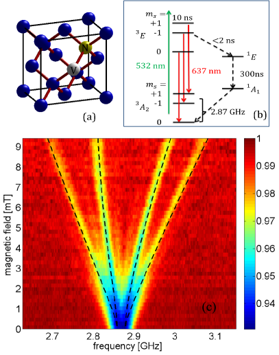
The defect has symmetry, leading to a triplet ground and excited states, with optical zero phonon line (ZPL) of (wavelength of . The sub-levels and of the ground state triplet are separated by in the absence of magnetic field [see Fig. 1(b)]. Note that denotes the spin along the axis [see Fig. 1(a)]. The excited state is a triplet as well, with zero-field splitting of .
The defect can be excited using green light (laser having wavelength of is employed in the current experiment). Once optically excited in the state, the defect can relax either through the same radiative transition, which gives rise to red photoluminescence (PL), or through a secondary path involving non-radiative intersystem crossing to singlet states, as can be seen in Fig. 1(b). While optical transitions are spin conserving, these non-radiative crossings are strongly spin selective, as the shelving rate from sublevel is much slower than those from . In addition, the defect decays preferentially from the lowest singlet state towards the ground state sublevel. These spin selective processes allow spin polarization into through optical pumping. Furthermore, since intersystem crossings are non-radiative, the defect PL is significantly higher when the state is populated. Such a spin-dependent PL response enables the detection of electron spin resonance (ESR) by optical means Gruber et al. (1997).
The ground state spin Hamiltonian of the NV- defect in diamond is given by , where the direction is taken to be parallel to the axis, the parallel part is given by , the transverse part is given by , is the magnetic field in the direction, where , is the corresponding spin matrix, and are axial and off-axial zero-field splitting parameters, respectively, is Landé g-factor, is Planck constant and is Bohr magneton Doherty et al. (2013). By evaluating the eigenvalues of using perturbation theory, one finds for the case where that the resonance frequencies corresponding to the transitions are given by Rondin et al. (2014)
| (1) |
where is the electron spin gyromagnetic ratio, and .
The NV defects in a single crystal diamond are oriented along the four lattice vectors , , and . The ODMR data seen in panel (c) of Fig. 1 has been obtained with externally applied magnetic field having a vanishing component in the direction, and consequently only 4 resonances are obtained. The dashed lines in Fig. 1(c) represent the frequencies calculated according to Eq. (1). In general, the term proportional to in Eq. (1) can be disregarded when . Note, however, that the comparison between the ODMR data seen in Fig. 1(c) and theory yields poor agreement when this term is disregarded. As can be seen from Eq. (1), diamond magnetometry becomes insensitive to when .
Our prototype diamond magnetometer is designed to allow magnetic imaging of an electrically wired sample at cryogenic temperatures. Sketch of the experimental setup is shown in Fig. 2(a). Laser cutting is used to shape a single crystal type Ib diamond into a thick disk having a diameter of . Electron irradiation at is employed using transmission electron microscope to create defects in the diamond disk. The electron irradiation is followed by annealing at for 1 hour and cleaning with boiling Perchloric acid, Nitric acid and Sulfuric acid for 1 hour.
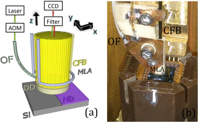
Optical adhesive is then used to glue the diamond disk to the tip of a glass-made coherent fiber bundle (CFB) having 30,000 cores, which allows optical imaging. A magnetometer probing head (see Fig. 2) integrates the CFB, a microwave loop antenna (MLA) and an additional multimode optical fiber (OF), which is used for guiding the laser light at a wavelength of into the CFB. Note that total internal reflection at the bottom interface of the diamond disk prevents the laser light from reaching the sample under study, avoiding thus undesired heating due to optical absorption by the sample. The electrically wired sample is mounted on a 5-axis piezoelectric positioner having a sub nanometer resolution, allowing reaching contact between the sample and the diamond disk. A charge-coupled device (CCD) camera and a complementary metal-oxide semiconductor (CMOS) one are employed for ODMR imaging of the emitted red photons (long pass dichroic mirror with a cutoff wavelength of is used).
A niobium film having a rectangular shape, an area of and thickness of has been deposited on a high resistivity Si/SiN substrate through a mechanical mask using DC-magnetron sputtering. Magnetometry measurements of the film, whose critical temperature is , are performed at temperature of . A superconducting solenoid is employed for applying a uniform magnetic field perpendicularly to the film. The measured ODMR signal is presented in Fig. 3 for various values of the externally applied magnetic field.
The current distribution in a thin film type-II superconductor under applied bias magnetic field is theoretically evaluated by employing the critical state model Bean (1962); Navau et al. (2013). In this model the sheet current density is only allowed to be as high as the critical value . For the case of a constant , the sheet current distribution is found to be given by Brandt et al. (1993); Zeldov et al. (1994)
| (2) |
where is the width of the stripe, , and is the critical field. The bias field is applied along the axis, and the currents are along the axis, as defined in Fig. 2.
In general, due to flux trapping the current distribution is history dependent. For the case where the bias magnetic field is first risen from zero to a maximum value of , and then decreased to , the resulting current distribution is found to be given by Brandt et al. (1993)
| (3) |
After the current distribution is calculated according to Eqs. (2) and (3), the magnetic field in the whole space is computed by integrating the current density with the Biot-Savart kernel.
One of the simplifying assumptions that have been made in the derivation of Eqs. (2) and (3) is that is independent on the local value of the magnetic induction Brandt et al. (1993); Zeldov et al. (1994). More recently, however, various types of dependencies have been assumed, and the calculation of the current density has been generalized accordingly Bobyl et al. (2001); Del-Valle et al. (2011); Davey et al. (2013); Navau et al. (2013). In the so-called exponential model Fietz et al. (1964); Young et al. (2005) is taken to be given by
| (4) |
where is a characteristic field and is the sheet critical current in the low magnetic field limit. To account for the dependence of on the local value of we employed the method that has been presented in Ref. McDonald and Clem (1996) in order to calculate the theoretically predicted magnetic field that is generated by the superconducting film.
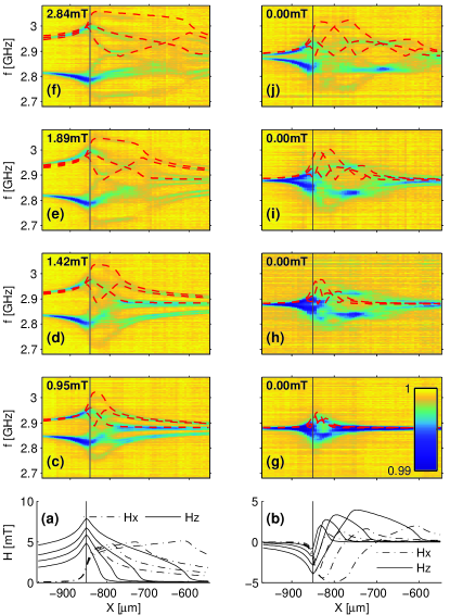
The diamond disk was positioned parallel to the sample, in contact with it, and the bias field was applied in the perpendicular direction. The spatial orientation of the diamond crystal with respect to the cartesian coordinate system that is defined in Fig. 2 is specified in terms of the unitary transformation , where () represents a rotation around the () axis with the rotation angle (). The transformation is applied to the initial orientation, for which the lattice vectors , and are taken to be parallel to the unit vectors , and , respectively, allowing thus the calculation of the 4 unit vectors pointing in the directions of NV defects in the diamond disk. Next, the frequencies are calculated for each unit vector using Eq. (1) (see the red dashed lines in Fig. 3(c)-(j), which represent the calculated values of ).
Comparison between the experimental results and theory is presented in Fig. 3. The ODMR data seen in panels (c)-(f) are obtained after first preparing the sample in the virgin state, and then applying a field , whereas the data seen in panels (g)-(j) are obtained after reducing the field down to zero. The red fit curves are calculated by assuming that is given by Eq. (4). The only fitting parameters that were not independently measured are and . In addition to the fitting that is presented in Fig. 3, which is based on the exponential model, other methods have been tested. We found that when the dependence of on the local value of is disregarded, i.e. when Eq. (2) is employed for calculating , acceptable agreement with experiment can be obtained in the region of low values of , however the discrepancy becomes significant at high values. Furthermore, the fitting procedure was tested when instead of the exponential model, the so-called Kim’s model Kim et al. (1963) has been employed to determine the dependency . By comparing the results we conclude that the exponential model yields a better (though, not a perfect) agreement with the experimental results.
In summary, the magnetic field generated by shielding currents in a thin superconducting niobium film has been measured. Our diamond magnetometer offers some unique advantages compared with alternative methods that have been previously employed for studying magnetic properties of superconductors Bending et al. (2004) (see the introductory paragraph above). As was already pointed out above, it allows simultaneous measurement of all three components of the magnetic field vector, and it exploits the effect of total internal reflection to allow low-temperature operation. Furthermore, magnetic field imaging over a large area can be performed without any mechanical scanning Hall et al. (2012). The sensitivity of our magnetometer is estimated to be . Further improvements in the design of the magnetometer may enable operation at ultra-low temperatures. Such ability may open the way for a variety of new applications, for example a single-shot quantum state readout of a large array of superconducting Josephson qubits Berkley et al. (2010).
We thank Ran Fischer, Nir Bar-Gill, Eli Zeldov and Rafi Kalish for extremely useful discussions. This work is supported by the Israel Science Foundation and by the Security Research Foundation in the Technion.
References
- Bending (1999) S. J. Bending, Advances in Physics 48, 449 (1999).
- Nakano et al. (2010) T. Nakano, N. Fujiwara, K. Tatsumi, H. Okada, H. Takahashi, Y. Kamihara, M. Hirano, and H. Hosono, Physical Review B 81, 100510 (2010).
- Mamin et al. (2007) H. Mamin, M. Poggio, C. Degen, and D. Rugar, Nature nanotechnology 2, 301 (2007).
- Chang et al. (1992) A. Chang, H. Hallen, L. Harriott, H. Hess, H. Kao, J. Kwo, R. Miller, R. Wolfe, J. Van der Ziel, and T. Chang, Applied Physics Letters 61, 1974 (1992).
- Lyard et al. (2004a) L. Lyard, P. Szabo, T. Klein, J. Marcus, C. Marcenat, K. Kim, B. Kang, H. Lee, and S. Lee, Physical review letters 92, 057001 (2004a).
- Lyard et al. (2004b) L. Lyard, T. Klein, J. Marcus, R. Brusetti, C. Marcenat, M. Konczykowski, V. Mosser, K. Kim, B. Kang, H. Lee, et al., Physical Review B 70, 180504 (2004b).
- Okazaki et al. (2009) R. Okazaki, M. Konczykowski, C. J. Van Der Beek, T. Kato, K. Hashimoto, M. Shimozawa, H. Shishido, M. Yamashita, M. Ishikado, H. Kito, et al., Physical Review B 79, 064520 (2009).
- Zeldov et al. (1995) E. Zeldov, D. Majer, M. Konczykowski, V. Geshkenbein, V. Vinokur, and H. Shtrikman, Nature 375, 373 (1995).
- Van der Beek et al. (2010) C. Van der Beek, G. Rizza, M. Konczykowski, P. Fertey, I. Monnet, T. Klein, R. Okazaki, M. Ishikado, H. Kito, A. Iyo, et al., Physical Review B 81, 174517 (2010).
- Abulafia et al. (1998) Y. Abulafia, M. McElfresh, A. Shaulov, Y. Yeshurun, Y. Paltiel, D. Majer, H. Shtrikman, and E. Zeldov, Applied Physics Letters 72, 2891 (1998).
- Oral et al. (1996) A. Oral, S. Bending, and M. Henini, Journal of Vacuum Science & Technology B 14, 1202 (1996).
- Dorosinskii et al. (1992) L. Dorosinskii, M. Indenbom, V. Nikitenko, Y. A. Ossip’yan, A. Polyanskii, and V. Vlasko-Vlasov, Physica C: Superconductivity 203, 149 (1992).
- Johansen et al. (1996) T. Johansen, M. Baziljevich, H. Bratsberg, Y. Galperin, P. Lindelof, Y. Shen, and P. Vase, Physical Review B 54, 16264 (1996).
- Jooss et al. (2002) C. Jooss, J. Albrecht, H. Kuhn, S. Leonhardt, and H. Kronmüller, Reports on progress in Physics 65, 651 (2002).
- Soibel et al. (2000) A. Soibel, E. Zeldov, M. Rappaport, Y. Myasoedov, T. Tamegai, S. Ooi, M. Konczykowski, and V. B. Geshkenbein, Nature 406, 282 (2000).
- Kirtley and Wikswo Jr (1999) J. R. Kirtley and J. P. Wikswo Jr, Annual Review of Materials Science 29, 117 (1999).
- Hasselbach et al. (2002) K. Hasselbach, D. Mailly, and J. Kirtley, Journal of applied physics 91, 4432 (2002).
- Kuit et al. (2008) K. Kuit, J. Kirtley, W. Van Der Veur, C. Molenaar, F. Roesthuis, A. Troeman, J. Clem, H. Hilgenkamp, H. Rogalla, and J. Flokstra, Physical Review B 77, 134504 (2008).
- Embon et al. (2015) L. Embon, Y. Anahory, A. Suhov, D. Halbertal, J. Cuppens, A. Yakovenko, A. Uri, Y. Myasoedov, M. L. Rappaport, M. E. Huber, et al., Scientific reports 5, 7598 (2015).
- Vasyukov et al. (2013) D. Vasyukov, Y. Anahory, L. Embon, D. Halbertal, J. Cuppens, L. Neeman, A. Finkler, Y. Segev, Y. Myasoedov, M. L. Rappaport, et al., Nature nanotechnology 8, 639 (2013).
- Luan et al. (2011) L. Luan, T. M. Lippman, C. W. Hicks, J. A. Bert, O. M. Auslaender, J.-H. Chu, J. G. Analytis, I. R. Fisher, and K. A. Moler, Physical review letters 106, 067001 (2011).
- Shapoval et al. (2011) T. Shapoval, H. Stopfel, S. Haindl, J. Engelmann, D. Inosov, B. Holzapfel, V. Neu, and L. Schultz, Physical Review B 83, 214517 (2011).
- Bean (1964) C. P. Bean, Reviews of Modern Physics 36, 31 (1964).
- Campbell and Evetts (1972) A. Campbell and J. Evetts, Advances in Physics 21, 199 (1972).
- Brandt et al. (1993) E. Brandt, M. Indenbom, and A. Forkl, Europhysics Letters 22, 735 (1993).
- Zeldov et al. (1994) E. Zeldov, J. R. Clem, M. McElfresh, and M. Darwin, Physical Review B 49, 9802 (1994).
- Fietz et al. (1964) W. Fietz, M. Beasley, J. Silcox, and W. Webb, Physical Review 136, A335 (1964).
- Doherty et al. (2013) M. W. Doherty, N. B. Manson, P. Delaney, F. Jelezko, J. Wrachtrup, and L. C. Hollenberg, Physics Reports 528, 1 (2013).
- Rondin et al. (2014) L. Rondin, J. Tetienne, T. Hingant, J. Roch, P. Maletinsky, and V. Jacques, Reports on Progress in Physics 77, 056503 (2014).
- Maze et al. (2008) J. Maze, P. Stanwix, J. Hodges, S. Hong, J. Taylor, P. Cappellaro, L. Jiang, M. G. Dutt, E. Togan, A. Zibrov, et al., Nature 455, 644 (2008).
- Balasubramanian et al. (2008) G. Balasubramanian, I. Chan, R. Kolesov, M. Al-Hmoud, J. Tisler, C. Shin, C. Kim, A. Wojcik, P. R. Hemmer, A. Krueger, et al., Nature 455, 648 (2008).
- Rondin et al. (2012) L. Rondin, J.-P. Tetienne, P. Spinicelli, C. Dal Savio, K. Karrai, G. Dantelle, A. Thiaville, S. Rohart, J.-F. Roch, and V. Jacques, Applied Physics Letters 100, 153118 (2012).
- Acosta et al. (2010a) V. Acosta, E. Bauch, A. Jarmola, L. Zipp, M. Ledbetter, and D. Budker, Applied Physics Letters 97, 174104 (2010a).
- Pham et al. (2011) L. M. Pham, D. Le Sage, P. L. Stanwix, T. K. Yeung, D. Glenn, A. Trifonov, P. Cappellaro, P. Hemmer, M. D. Lukin, H. Park, et al., New Journal of Physics 13, 045021 (2011).
- Balasubramanian et al. (2009) G. Balasubramanian, P. Neumann, D. Twitchen, M. Markham, R. Kolesov, N. Mizuochi, J. Isoya, J. Achard, J. Beck, J. Tissler, et al., Nature materials 8, 383 (2009).
- Steinert et al. (2010) S. Steinert, F. Dolde, P. Neumann, A. Aird, B. Naydenov, G. Balasubramanian, F. Jelezko, and J. Wrachtrup, Review of scientific instruments 81, 043705 (2010).
- Vershovskii and Dmitriev (2015a) A. Vershovskii and A. Dmitriev, Technical Physics Letters 41, 1026 (2015a).
- Vershovskii and Dmitriev (2015b) A. Vershovskii and A. Dmitriev, Technical Physics Letters 41, 393 (2015b).
- Gruber et al. (1997) A. Gruber, A. Dräbenstedt, C. Tietz, L. Fleury, J. Wrachtrup, and C. Von Borczyskowski, Science 276, 2012 (1997).
- Le Sage et al. (2012) D. Le Sage, L. M. Pham, N. Bar-Gill, C. Belthangady, M. D. Lukin, A. Yacoby, and R. L. Walsworth, Physical Review B 85, 121202 (2012).
- Harrison et al. (2006) J. Harrison, M. Sellars, and N. Manson, Diamond and related materials 15, 586 (2006).
- Grinolds et al. (2013) M. Grinolds, S. Hong, P. Maletinsky, L. Luan, M. Lukin, R. Walsworth, and A. Yacoby, Nature Physics 9, 215 (2013).
- Hall et al. (2012) L. Hall, G. Beart, E. Thomas, D. Simpson, L. McGuinness, J. Cole, J. Manton, R. Scholten, F. Jelezko, J. Wrachtrup, et al., Scientific reports 2 (2012).
- McGuinness et al. (2011) L. McGuinness, Y. Yan, A. Stacey, D. Simpson, L. Hall, D. Maclaurin, S. Prawer, P. Mulvaney, J. Wrachtrup, F. Caruso, et al., Nature nanotechnology 6, 358 (2011).
- Bouchard et al. (2011) L.-S. Bouchard, V. M. Acosta, E. Bauch, and D. Budker, New Journal of Physics 13, 025017 (2011).
- Waxman et al. (2014) A. Waxman, Y. Schlussel, D. Groswasser, V. Acosta, L.-S. Bouchard, D. Budker, and R. Folman, Physical Review B 89, 054509 (2014).
- Acosta et al. (2010b) V. Acosta, E. Bauch, M. Ledbetter, A. Waxman, L.-S. Bouchard, and D. Budker, Physical review letters 104, 070801 (2010b).
- Dolde et al. (2011) F. Dolde, H. Fedder, M. W. Doherty, T. Nöbauer, F. Rempp, G. Balasubramanian, T. Wolf, F. Reinhard, L. Hollenberg, F. Jelezko, et al., Nature Physics 7, 459 (2011).
- Maurer et al. (2012) P. C. Maurer, G. Kucsko, C. Latta, L. Jiang, N. Y. Yao, S. D. Bennett, F. Pastawski, D. Hunger, N. Chisholm, M. Markham, et al., Science 336, 1283 (2012).
- Cai et al. (2012) J. Cai, F. Jelezko, N. Katz, A. Retzker, and M. B. Plenio, New Journal of Physics 14, 093030 (2012).
- Huebener et al. (1975) R. Huebener, R. Kampwirth, R. Martin, T. Barbee, and R. Zubeck, IEEE Transactions on Magnetics 11, 344 (1975), ISSN 0018-9464.
- Kim et al. (2012) E. Kim, V. M. Acosta, E. Bauch, D. Budker, and P. R. Hemmer, Applied physics letters 101, 082410 (2012).
- Bean (1962) C. Bean, Physical Review Letters 8, 250 (1962).
- Navau et al. (2013) C. Navau, N. Del-Valle, and A. Sanchez, IEEE Transactions on Applied Superconductivity 23, 8201023 (2013).
- Bobyl et al. (2001) A. Bobyl, D. Shantsev, Y. Galperin, and T. Johansen, Physical Review B 63, 184510 (2001).
- Del-Valle et al. (2011) N. Del-Valle, C. Navau, A. Sanchez, and D.-X. Chen, Applied Physics Letters 98, 202506 (2011).
- Davey et al. (2013) K. R. Davey, R. Weinstein, D. Parks, and R.-P. Sawh, IEEE Transactions on Magnetics 49, 1153 (2013).
- Young et al. (2005) D. Young, M. Moldovan, P. Adams, and R. Prozorov, Superconductor Science and Technology 18, 776 (2005).
- McDonald and Clem (1996) J. McDonald and J. R. Clem, Physical Review B 53, 8643 (1996).
- Kim et al. (1963) Y. Kim, C. Hempstead, and A. Strnad, Physical Review 129, 528 (1963).
- Bending et al. (2004) S. Bending, A. Brook, J. Gregory, I. Crisan, A. Pross, A. Grigorenko, A. Oral, F. Laviano, and E. Mezzetti, in Magneto-Optical Imaging (Springer, 2004), pp. 11–18.
- Berkley et al. (2010) A. Berkley, M. Johnson, P. Bunyk, R. Harris, J. Johansson, T. Lanting, E. Ladizinsky, E. Tolkacheva, M. Amin, and G. Rose, Superconductor Science and Technology 23, 105014 (2010).