Emergence of topological bands on the surface of ZrSnTe crystal
Abstract
By using angle-resolved photoemission spectroscopy combined with first-principles calculations, we reveal that the topmost unit cell of ZrSnTe crystal hosts two-dimensional (2D) electronic bands of topological insulator (TI) state, though such a TI state is defined with a curved Fermi level instead of a global band gap. Furthermore, we find that by modifying the dangling bonds on the surface through hydrogenation, this 2D band structure can be manipulated so that the expected global energy gap is most likely to be realized. This facilitates the practical applications of 2D TI in heterostructural devices and those with surface decoration and coverage. Since ZrSnTe belongs to a large family of compounds having the similar crystal and band structures, our findings shed light on identifying more 2D TI candidates and superconductor-TI heterojunctions supporting topological superconductors.
pacs:
73.20.-r, 71.20.-b, 79.60.-iAfter nearly a decade of intensive studies, the field of topological insulators (TIs) has led to remarkable achievements Hasan2010 ; Qi2011 ; Weng2014 , such as the discoveries of two-dimensional (2D) Bernevig2006 ; Konig2007 ; Knez2011 and three-dimensional (3D) TIs Chen2009 , quantum anomalous Hall effect (or Chern insulators) Yu2010 ; Chang2013 ; Wengadv2015 , topological crystalline insulators Fu2011 ; Heish2012NC and even topological semimetals like Dirac semimetals Wang2012&2013 ; Liu2014 ; Liu2014a and Weyl semimetals Weng2015Weyl ; Lv2015 ; Huang2015 ; Xu2015Weyl ; Lv2015a ; Xu2015Weyla . However, when looking back one finds that the study of 2D TIs is still at the early stage it was when it ignited the whole field. 2D TIs have more promising potential applications than their 3D cousins Ando2013 . The lack of experimentally suitable 2D TI materials is the main problem. A favorable 2D TI is expected to have a quite large band gap to be operable under easily accessible temperature and to be prepared easily Weng2014 . Considerable theoretical efforts have predicted many 2D TI candidates in recent years Weng2014PRX ; BiRhI ; Bi4Br4 ; KHgSb ; Tin , but few of them has been confirmed experimentally.
Very recently, Xu . have proposed that ZrSiO monolayer is a 2D TI with a band gap up to 30 meV, and that its isostructural compounds ( = Zr, Hf, or La, = Si, Ge, Sn, or Sb, and = O, S, Se, and Te) possess similar electronic structures Xu2015 . It is also proposed that if the inherent spin-orbit coupling (SOC) is neglected, they are node-line semimetals Xu2015 ; ZrSiS2015 . In this work, we report systematic angle-resolved photoemission spectroscopy (ARPES) measurements on ZrSnTe single crystals. By comparing with first-principles calculations, we reveal that the topmost unit cell on the (001) surface hosts a 2D electronic structure, which is significantly consistent with that of the proposed 2D TI ZrSnTe monolayer. However, such a 2D TI state is defined with a curved Fermi level () instead of a global band gap to ensure a finite gap at each crystal momentum point. We further prove that such topological bands can be engineered by modifying the dangling bonds on the terminating layer. The hydrogenation of the dangling bonds of Zr 4 orbitals tends to align the band gaps to the same energy level. This observation is excellently reproduced by our slab calculations, which predict that a global band gap can be reached at 0.5 eV above the chemical potential as all the Zr ions on the terminating layer are bonded with hydrogen. Our findings suggest that the series is a plausible platform to support 2D TI with nontrivial electronic bands, for which the surface decoration, or interface of heterostructure can realize a global band gap, which is more suitable for the practical device application than free-standing 2D systems.
High-quality single crystals of ZrSnTe were grown by the Te flux method. ARPES measurements were performed at the “Dreamline” beamline of the Shanghai Synchrotron Radiation Facility (SSRF) with a Scienta D80 analyzer, and at the beamline 13U of the National Synchrotron Radiation Laboratory (NSRL) with a Scienta R4000 analyzer. The samples were cleaved and measured at = 20–40 K in a vacuum better than 510-11 Torr. The energy and angular resolutions were set to 15 meV and 0.2∘, respectively. The ARPES data were collected using horizontally polarized light with a vertical analyzer slit. The hydrogen adsorption process was controlled by exposing samples in vacuum for a longer time at the lowest temperature 20 K. In contrast, no noticeable changes in the spectra were observed during the regular measurements at = 40 K. Most of the first-principles calculations were carried out using the Vienna simulation package (VASP) Kresse1996a . A detailed description of the sample growth and theoretical calculation can be found in the Supplemental Materials Supplemental .

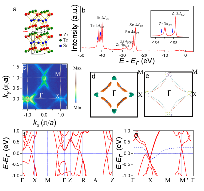
ZrSnTe crystallizes in a PbFCl-type crystal structure with space group 4/ Wang1995 , in which Sn is located at the center of a tetrahedron consisting of Zr atoms, as illustrated in Fig. 1a. It is isostructural to the well known ‘111’ type iron-based superconductor LiFeAs Wang2008 . The relatively weak Zr-Te bonding between two neighboring slabs provides a natural cleavage plane between the adjacent ZrTe layers, which yields a (001) surface with Zr and Te termination. This is consistent with the core level spectrum in Fig. 1b, in which the double peaks of Te 4 and 4 split further into a total of four peaks. In the inset of Fig. 1b, the Zr 3 and 3 peaks exhibit shoulders on the higher binding energy side. These indicate that the chemical environments of the Te and Zr ions in the terminating layer are different from those inside. The measured Fermi surfaces (FSs) in Fig. 1c consist of small electron pockets at and “lenses”-like hole pockets in the – direction. Such a FS topology is distinctly different from the calculations of bulk ZrSnTe in Fig. 1d, in which there is no FS centered around . In contrast, it looks very similar to that of monolayer ZrSnTe in Fig. 1e.
The most distinct difference in the calculated electronic structures between the bulk (Fig. 1f) and the free-standing monolayer (Fig. 1g) is that the electron bands at are shifted down by 1 eV, forming two electron pockets centered at in the monolayer. This arises from the dangling bond of the Zr 4 and 4+4 orbitals in the monolayer (see Supplemental Materials Supplemental ). In bulk ZrSnTe, these Zr 4 orbitals are bonded with the Te 5 and Zr 4 orbitals in the adjacent unit cell along the (001) direction. As discussed in Ref. Xu2015, , the Dirac cone-like bands around in both the = 0 and planes will open gap when SOC is included since these bands have the same irreducible representation. Similarly, SOC opens band gaps at (75 meV) and (80 meV) on the path – in the monolayer ZrSnTe in Fig. 1g. As the gaps are located at different energies, we use a dashed curve to represent the fictitious Fermi level. Thus, the number is well defined for the bands below the curved Fermi level since there is a finite band gap at each -point. It is determined to be 1 by counting the parity of all occupied states at four time-reversal-invariant momenta. These indicate that the monolayer ZrSnTe could be a 2D TI once the curved Fermi level is straightened by band manipulation as discussed in the following.

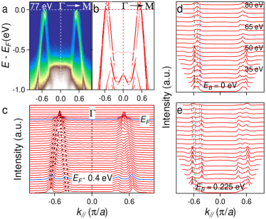
In order to illuminate the topological character of the measured electronic structure, we have investigated the band dispersions along the high-symmetry lines –, –, and –. The band structure along – is shown in Fig. 2. The intensity plot in Fig. 2a exhibits a Dirac-like band structure with crossing points near . The cone-like feature is consistent with the monolayer and bulk calculations. From the momentum distribution curves (MDCs) in Fig. 2c, one can see that each branch of the cone consists of two or three nearly parallel bands. The multiple bands feature was reproducible in several measured samples, which rules out the possibility of extrinsic effects such as multiple terraces on the cleavage surfaces or faults in the crystals. The feature is further confirmed by the multiple peaks in the MDCs taken with different photon energies (Figs. 2d and 2e). The extra bands are not reproduced by either the monolayer or bulk calculations. To understand the experimental observation, we have performed a slab model calculation for a thickness of seven unit cells along the lattice. The slab model calculation is a good way to simulate the real sample situation in ARPES measurements Lv2015 ; Lv2015a . The calculated band dispersions with spectral weight from the top two unit cells are plotted in Fig. 2b, which can reproduce the experimental bands very well and indicate that the ARPES experiments detect the signals of escaped photoelectrons mainly from the top two unit cells. The outmost Zr atoms have different chemical environment from those inside, causing the slightly split parallel bands.


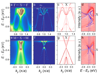
The band structures along – and – are summarized in Fig. 3. We clearly observe a non-degenerate Dirac cone-like band structure with a band gap of 90 meV at , as seen in Figs. 3d and 3h. This observation is well consistent with the monolayer calculations presented in Fig. 1g. In addition to the Dirac cone-like bands, we distinguish three near- bands along –, as seen in Fig. 3b. The outmost band () disperses almost linearly and crosses at 0.64 / while the other two bands ( and ) turn back at binding energy 80 and 150 meV, respectively. They are overlapped at = 0.3 eV at . Likewise, these experimental bands are well reproduced by the slab model calculation with spectral weight from the top two unit cells in Figs. 3c and 3g. We note that the electron band, as well as the and bands, are mainly contributed by the spectral weight from the top one unit cell. By summarizing the band dispersions along the high-symmetry lines, it is concluded that the 3D ZrSnTe crystals host a 2D electronic state in the topmost unit cell, which is close to that of the free-standing monolayer.
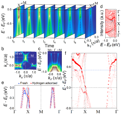
As in the case of the monolayer, the dangling bond from the Zr 4 orbitals in the topmost unit cell causes the down-shift of the electron bands at . One can manipulate these bands by modifying the chemical environment of these Zr through surface decoration/coverage, or interface of heterostructure. Hydrogenation has been found as an effective method to modify the electronic properties of graphene and silicene graphene3 ; silicene1 . We have investigated the effects of hydrogenation on these bands of the topmost unit cell using the residual hydrogen gas, which is the main component in the main chamber of our ARPES system with a pressure of 310-11 Torr, as measured by the residual gas analyzer. We find that the bands near associated with the Zr 4 dangling orbitals are sensitive to the hydrogen adsorption on the surface. As seen in Fig. 4a, the bands composed of the dangling orbitals around steadily moves up with time, and eventually the valence band top reaches the vicinity of when keeping the samples at = 20 K. In contrast, the band dispersions along – only change slightly in Fig. 4c. The changes in the band structure are further confirmed by the FS intensity plot in Fig. 4b, in which the electron pocket at in Fig. 1c disappears while the “lenses”-like hole pockets along – are little changed.
Since the sensitivity of the energy gaps to the hydrogen adsorption at and is different, the energy levels of the two gaps might become the same by controlling the hydrogen adsorption process. We have performed similar slab calculation but with the surface Zr ions all bonded with hydrogen atoms. The band structure with spectral weight on the topmost unit cell is shown in Fig. 4f. Firstly, the weighted band structure can well reproduce the most characteristic features observed in the hydrogenated sample shown in Fig. 4e, such as the valence band top near around and the nearly unchanged hole pocket along –. Secondly, there are electrons transferred from the surface Zr to the hydrogen atoms to form occupied bonding states, causing the up-shift of the bands associated with the Zr 4 orbitals. Thirdly, the two gaps along – and – are located at the same energy level of 0.5 eV above , although the band gap is quite small. We would like to stress that as discussed in Ref. Xu2015, , these bands have the same irreducible representation in bulk. The symmetry is further lowered on the (001) surface, which leads to definite band gap opening. Therefore, an ideal 2D TI with a global band gap in the topmost layer is to be realized by such modification of the surface termination.
In conclusion, our results have confirmed the existence of 2D topological electronic bands on the surface of ZrSnTe crystal. We have also demonstrated that the surface decoration, such as hydrogenation, is a promising way to manipulating these bands to open a global band gap. This brings us a high chance to achieve an ideal 2D TI, through the similar surface decoration or interface of heterostructures, among the predicted family Xu2015 . Actually, our previous calculations have predicted that ZrSiO and LaSbTe would be an ideal 2D TI with a global gap located at Xu2015 . The tunable 2D TI states in covered or decorated top surface, as well as the fact that it is isostructural to the iron-based superconductor LiFeAs Wang2008 , bring great promises in fabricating superconductor-TI heterostructures, in which various extraordinary quantum phenomena, , topological superconductivity and Majorana modes, could be induced by the superconducting proximity effect Qi2011 ; Fu2008 .
This work was supported by the Ministry of Science and Technology of China (Nos 2011CBA00108, 2012CB921701, 2013CB921700, and 2015CB921300), the National Natural Science Foundation of China (Nos 11274381, 11274359, 11422428, 11474340, and 11574394), and the Chinese Academy of Sciences (No. XDB07000000).
Note added.—During the review of this paper, there have been six preprints ZrSiS1 ; ZrSiS2 ; ZrSiS3 ; ZrSiS4 ; ZrSiS5 ; ZrSiS6 reporting the transport and ARPES measurements on ZrSiS, which shares the similar crystal structure and electronic structure as ZrSnTe.
References
- (1) M. Z. Hasan and C. L. Kane, Rev. Mod. Phys. 82, 3045 (2010).
- (2) X. L. Qi and S. C. Zhang, Rev. Mod. Phys. 83, 1057 (2011).
- (3) H. Weng, X. Dai, and Z. Fang, MRS Bulletin 39, 849 (2014).
- (4) B. A. Bernevig, T. L. Hughes, and S. C. Zhang, Science 314, 1757 (2006).
- (5) M. König, S. Wiedmann, C. Brüne, A. Roth, H. Buhmann, L. W. Molenkamp, X.-L. Qi, and S.-C. Zhang, Science 318, 766 (2007).
- (6) I. Knez, R.-R. Du, and G. Sullivan, Phys. Rev. Lett. 107, 136603 (2011).
- (7) Y. L. Chen, J. G. Analytis, J.-H. Chu, Z. K. Liu, S.-K. Mo, X. L. Qi, H. J. Zhang, D. H. Lu, X. Dai, Z. Fang, S. C. Zhang, I. R. Fisher, Z. Hussain, and Z.-X. Shen, Science 325, 178 (2009).
- (8) R. Yu, W. Zhang, H. Zhang, S.-C. Zhang, X. Dai, and Z. Fang, Science 329, 5987 (2010).
- (9) C.-Z. Chang, J. Zhang, X. Feng, J. Shen, Z. Zhang, M. Guo, K. Li, Y. Ou, P. Wei, L.-L. Wang, Z.-Q. Ji, Y. Feng, S. Ji, X. Chen, J. Jia, X. Dai, Z. Fang, S.-C. Zhang, K. He, Y. Wang, L. Lu, X.-C. Ma, and Q.-K. Xue, Science 340, 167 (2013).
- (10) H. Weng, R. Yu, X. Hu, X. Dai, and Z. Fang, Adv. Phys. 64, 227 (2015).
- (11) L. Fu, Phys. Rev. Lett. 106, 106802 (2011).
- (12) T. H. Hsieh, H. Lin, J. Liu, W. Duan, A. Bansil, and L. Fu, Nat. Commun. 3, 982 (2012).
- (13) Z. Wang, Y. Sun, X.-Q. Chen, C. Franchini, G. Xu, H. Weng, X. Dai, and Z. Fang, Phys. Rev. B 85, 195320 (2012); Z. Wang, H. Weng, Q. Wu, X. Dai, and Z. Fang, Phys. Rev. B 88, 125427 (2013).
- (14) Z. K. Liu, B. Zhou, Y. Zhang, Z. J. Wang, H. Weng, D. Prabhakaran, S.-K.Mo, Z. X. Shen, Z. Fang, X. Dai, Z. Hussain, and Y. L. Chen, Science 343, 864 (2014).
- (15) Z. K. Liu, J. Jiang, B. Zhou, Z. J. Wang, Y. Zhang, H. M. Weng, D. Prabhakaran, S. K. Mo, H. Peng, P. Dudin, T. Kim, M. Hoesch, Z. Fang, X. Dai, Z.-X. Shen, D. L. Feng, Z. Hussain, and Y. L. Chen, Nat. Mater. 13, 677 (2014).
- (16) H. Weng, C. Fang, Z. Fang, B. A. Bernevig, and X. Dai, Phys. Rev. X 5, 011029 (2015).
- (17) B. Q. Lv, H. M. Weng, B. B. Fu, X. P. Wang, H. Miao, J. Ma, P. Richard, X. C. Huang, L. X. Zhao, G. F. Chen, Z. Fang, X. Dai, T. Qian, and H. Ding, Phys. Rev. X 5, 031013 (2015).
- (18) S. Huang, S. Xu, I. Belopolski, C. Lee, G. Chang, B. Wang, N. Alidoust, G. Bian, M. Neupane, C. Zhang, S. Jia, A. Bansil, H. Lin, and M. Z. Hasan, Nat. Commun. 6, 7373 (2015).
- (19) S. Xu, I. Belopolski, N. Alidoust, Madhab Neupane, G. Bian, C. Zhang, R. Sankar, G. Chang, Z. Yuan, C. Lee, S. Huang, H. Zheng, J. Ma, D. S. Sanchez, B. Wang, A. Bansil, F. Chou, P. P. Shibayev, H. Lin, S. Jia, M. Z. Hasan, Science 349, 613 (2015).
- (20) B. Q. Lv, N. Xu, H. M.Weng, J. Z. Ma, P. Richard, X. C. Huang, L. X. Zhao, G. F. Chen, C. Matt, F. Bisti, V. Strokov, J. Mesot, Z. Fang, X. Dai, T. Qian, M. Shi, and H. Ding, Nat. Phys. 11, 724 (2015).
- (21) S. Xu, N. Alidoust, I. Belopolski, Z. Yuan, G. Bian, T. Chang, H. Zheng, V. N. Strocov, D. S. Sanchez, G. Chang, C. Zhang, D. Mou, Y. Wu, L. Huang, C. Lee, S. Huang, B. Wang, A. Bansil, H. Jeng, T. Neupert, A. Kaminski, H. Lin, S. Jia, and M. Z. Hasan, Nat. Phys. 11, 748 (2015).
- (22) Y. Ando, J. Phys. Soc. Jpn. 82, 102001 (2013).
- (23) H. Weng, X. Dai, and Z. Fang, Phys. Rev. X 4, 011002 (2014).
- (24) B. Rasche et al., Nat. Mater. 12, 422 (2013); C. Pauly, B. Rasche, K. Koepernik, M. Liebmann, M. Pratzer, M. Richter, J. Kellner, M. Eschbach, B. Kaufmann, L. Plucinski, C. M. Schneider, M. Ruck, J. van den Brink, and M. Morgenstern, Nat. Phys. 11, 338 (2015).
- (25) B. Yan, L. Müchler, and C. Felser, Phys. Rev. Lett. 109, 116406 (2012).
- (26) J.-J. Zhou, W. Feng, C.-C. Liu, S. Guan, Y. Yao, Nano Lett. 14, 4767 (2014).
- (27) Y. Xu, B. Yan, H.-J. Zhang, J. Wang, G. Xu, P. Tang, W. Duan, S.-C. Zhang, Phys. Rev. Lett. 111, 136804 (2013); C.-C. Liu, H. Jiang, Y. Yao, Phys. Rev. B 84, 195430 (2011).
- (28) Q. Xu, Z. Song, S. Nie, H. Weng, Z. Fang, and X. Dai, Phys. Rev. B 92, 205310 (2015).
- (29) L. M. Schoop, M. N. Ali, C. Straer, V. Duppel, S. S. P. Parkin, B. V. Lotsch, and C. R. Ast, arXiv:1509.00861.
- (30) G. Kresse and J. Furthmüller, Comput. Mater. Sci. 6, 15 (1996).
- (31) See Supplemental Materials for detailed descriptions of the sample growth and theoretical calculation, and the slab calculation identifying the orbital character of dangling bonds.
- (32) C. Wang and T. Hughbanks, Inorg. Chem. 34, 5524 (1995).
- (33) X. C. Wang, Q. Q. Liu, Y. X. Lv, W. B. Gao, L. X. Yang, R. C. Yu, F. Y. Li, and C. Q. Jin, Solid State Commun. 148, 538 (2008).
- (34) R. Balog, B. Jrgensen, L. Nilsson, M. Andersen, E. Rienks, M. Bianchi, M. Fanetti, E. Lgsgaard, A. Baraldi, S. Lizzit, Z. Sljivancanin, F. Besenbacher, B. Hammer, T. G. Pedersen, P. Hofmann, and L. Hornekr, Nature Mater. 9, 315 (2010).
- (35) J. Qiu, H. Fu, Y. Xu, A. I. Oreshkin, T. Shao, H. Li, S. Meng, L. Chen, and K. Wu, Phys. Rev. Lett. 114, 126101 (2015).
- (36) L. Fu and C. L. Kane, Phys. Rev. Lett. 100, 096407 (2008).
- (37) R. Singha, A. Pariari, B. Satpati, and P. Mandal, arXiv:1602.01993.
- (38) M. N. Ali, L. M. Schoop, C. Garg, J. M. Lippmann, E. Lara, B. Lotsch, and S. Parkin, arXiv:1603.09318.
- (39) X. Wang, X. Pan, M. Gao, J. Yu, J. Jiang, J. Zhang, H. Zuo, M. Zhang, Z. Wei, W. Niu, Z. Xia, X. Wan, Y. Chen, F. Song, Y. Xu, B. Wang, G. Wang, and R. Zhang, arXiv:1604.00108.
- (40) M. Neupane, I. Belopolski, M. M. Hosen, D. S. Sanchez, R. Sankar, M. Szlawska, S. Y. Xu, K. Dimitri, N. Dhakal, P. Maldonado, P. M. Oppeneer, D. Kaczorowski, F. Chou, M. Z. Hasan, and T. Durakiewicz, Phys. Rev. B 93, 201104 (2016).
- (41) J. Hu, Z. Tang, J. Liu, Y. Zhu, J. Wei, and Z. Mao, arXiv:1604.01567.
- (42) Y. Lv, B. Zhang, X. Li, S. Yao, Y. B. Chen, J. Zhou, S. Zhang, M. Lu, and Y. Chen, arXiv:1604.01864.