Near-field integration of a SiN nanobeam and a SiO2 microcavity
for Heisenberg-limited displacement sensing
Abstract
Placing a nanomechanical object in the evanescent near-field of a high- optical microcavity gives access to strong gradient forces and quantum-noise-limited displacement readout, offering an attractive platform for precision sensing technology and basic quantum optics research. Robustly implementing this platform is challenging, however, as it requires separating optically smooth surfaces by . Here we describe a fully-integrated evanescent opto-nanomechanical transducer based on a high-stress Si3N4 nanobeam monolithically suspended above a SiO2 microdisk cavity. Employing a novel vertical integration technique based on planarized sacrificial layers, we achieve beam-disk gaps as little as 25 nm while maintaining mechanical Hz and intrinsic optical . The combined low loss, small gap, and parallel-plane geometry result in exceptionally efficient transduction, characterizing by radio-frequency flexural modes with vacuum optomechanical coupling rates of 100 kHz, single-photon cooperativities in excess of unity, and zero-point frequency (displacement) noise amplitudes of 10 kHz (fm)/Hz. In conjunction with the high power handling capacity of SiO2 and low extraneous substrate noise, the transducer operates particularly well as a sensor. Deploying it in a 4 K cryostat, we recently demonstrated a displacement imprecision 40 dB below that at the standard quantum limit (SQL) with an imprecision-back-action product . In this report we provide a comprehensive description of device design, fabrication, and characterization, with an emphasis on extending Heisenberg-limited readout to room temperature. Towards this end, we describe a room temperature experiment in which a displacement imprecision 30 dB below that at the SQL and an imprecision-back-action product is achieved. Our results impact the outlook for measurement-based quantum control of nanomechanical oscillators and offer perspective on the engineering of functionally-integrated (“hybrid”) optomechanical systems.
I Introduction

Nanomechanical oscillators Ekinci and Roukes (2005) are sensitive to weak forces and exhibit large zero-point fluctuations, making them an attractive platform for both precision sensing technology Cleland and Roukes (1998); Mamin and Rugar (2001); Jensen et al. (2008) and basic quantum science Schwab and Roukes (2005). Much effort has been devoted to the development of nanomechanical transducers in the electrical domain, including single-electron transistors LaHaye (2004), atomic point contacts Flowers-Jacobs et al. (2007), and superconducting microwave cavities Regal et al. (2008). Though very successful in recent years Teufel et al. (2011), these techniques are practically limited by the need for cryogenic operation. A comparatively powerful approach is to parametrically couple a nanomechanical oscillator to an optical cavity. The field of a laser-driven cavity can be quantum-noise-limited at room temperature, and as such represents a practically ideal form of mechanical transducer, with read out enabled by standard interferometric techniques and actuation provided by radiation pressure. Moreover, the finite build-up time of the cavity field allows it to do work on the mechanical element, enabling low-noise optical cooling and amplification Kippenberg and Vahala (2008). Investigation of these effects has led to two paradigmatic goals in the contemporary field of cavity optomechanics Aspelmeyer et al. (2014): cooling of a solid-state mechanical oscillator to its ground state and, concomitantly, read-out of its zero-point motion with the minimal disturbance allowed by the Heisenberg uncertainty principle (due to radiation pressure shot noise (RPSN) Caves (1980)). The first challenge has been met by several cryogenic optomechanical Chan et al. (2011); Verhagen et al. (2012) and electromechanical systems Teufel, J. D. et. al. (2011) (via resolved-sideband cooling Wilson-Rae et al. (2007)). The latter, corresponding to a measurement at the standard quantum limit (SQL) Braginsky and Braginskiĭ , remains outstanding; however, readout noise far below the zero-point displacement has been reported Wilson et al. (2015); Krause et al. (2015), as well as RPSN dominating the thermal force Purdy et al. (2013a); Teufel et al. (2016). Reaching the SQL ultimately requires a ‘Heisenberg-limited’ displacement sensor for which the product of the read out noise and the total force noise is the minimum allowed by the uncertainty principle. This regime has been approached to within an order of magnitude by several cryogenic systems Teufel, J. D. et. al. (2011); Wilson et al. (2015); it also forms the basis for measurement-based quantum feedback protocols such as ground-state cooling Wilson et al. (2015); Courty et al. (2001) and squeezing Szorkovszky et al. (2011) of an oscillator.
Efficient cavity optomechanical transduction involves co-localization of optical and mechanical modes with high and high optical power handling capacity. Moreover, it is desirable that the cavity support a mechanism for efficient input/output coupling. A diverse zoo (Fig. 2) of micro- and nanoscale cavity optomechanical systems (COMS) has risen to meet these challenges, ranging from cantilevers Kleckner and Bouwmeester (2006) and membranes Thompson et al. (2008) coupled to Fabry-Pérot cavities to mechanically-compliant whispering-gallery-mode (WGM) microcavities Schliesser et al. (2008) and photonic crystals Eichenfield et al. (2009). They generally employ two types of radiation pressure force coupling: traditional scattering-type coupling, in which the cavity field exchanges energy with the mechanical element via momentum transfer, and gradient force coupling Van Thourhout and Roels (2010), in which energy is exchanged via induced-dipole coupling to a field gradient. The net effect is a parametric coupling between the cavity resonance frequency and the mechanical degree of freedom , which expresses the force applied per intracavity photon, Aspelmeyer et al. (2014).
A particularly promising platform for optomechanical transduction involves placing a (dielectric) mechanical substrate next to the surface of a WGM microcavity, so that it samples its evanescent field. Since the evanescent decay length is , this topology offers the opportunity for strong gradient force coupling to nanoscale mechanical devices. It also has the virtue of naturally accommodating optical and mechanical substrates of dissimilar material and geometry, enabling separate optimization of . Moreover, WGMs can be input/output coupled with high ideality using tapered optical fibers Spillane et al. (2003), making them well-suited to interferometric displacement sensing. Recent work has focused on coupling of nano-beams Anetsberger et al. (2009), -cantilevers Doolin et al. (2014), and -membranes Anetsberger et al. (2009); Cole et al. (2015) to the evanescence of WGM micro-toroids Anetsberger et al. (2009), -spheres Neuhaus et al. (2012); Cole et al. (2015), and -disks Gavartin et al. (2012); Doolin et al. (2014), with mechanical materials ranging from (ultra low loss) high-stress Si3N4 Anetsberger et al. (2009) to (ultra low mass) single-layer graphene Cole et al. (2015), typically using SiO2 as the optical material. Gradient force coupling as high as MHz/nm has been achieved Anetsberger et al. (2009). Combined with the high power handling capacity of SiO2 and low extraneous displacement noise (typically thermo-refractive noise (TRN) in the cavity substrate Anetsberger et al. (2010)), optimized systems have achieved room temperature displacement imprecisions as low as , sufficient to in principle resolve the zero-point motion in one report Anetsberger et al. (2010).
Despite these advances, the full potential of evanescent cavity optomechanics has been inhibited by the difficulty of positioning the nanomechanical element within nm of the cavity substrate. Early systems made use of nanopositioning stages and suffered from vibrational stability Anetsberger et al. (2009). Gavartin et. al. Gavartin et al. (2012) addressed this challenge by integrating a Si3N4 nanobeam and a SiO2 microdisk on a chip; however, due to fabrication constraints, the beam-disk separation was limited to 250 nm and the optical was reduced by a factor of .
In this work, we discuss a novel method to monolithically integrate a high-stress Si3N4 thin film resonator and a SiO2 microdisk cavity within the evanescent near-field, without deteriorating the intrinsic of either element. The critical ingredient is a chemical mechanical polishing technique that allows integration of optically flat surfaces with sub-100 nm spacing, separated by a sacrificial film. This procedure is used to carefully isolate Si3N4 and SiO2 layers during wafer processing, allowing high-yield and deterministic fabrication of devices in which a nanobeam is monolithically suspended as little as 25 nm above a SiO2 microdisk — smaller than the evanescent decay length of its WGMs — while maintaining mechanical and optical mode qualities in excess of and , respectively. The process is compatible with e-beam lithography, thus we are able to locally pattern the beam with sub-10 nm imprecision (opening the door to stress engineering Norte et al. (2015)) and laterally position it with sub-100 nm imprecision across a full 4” Si wafer.
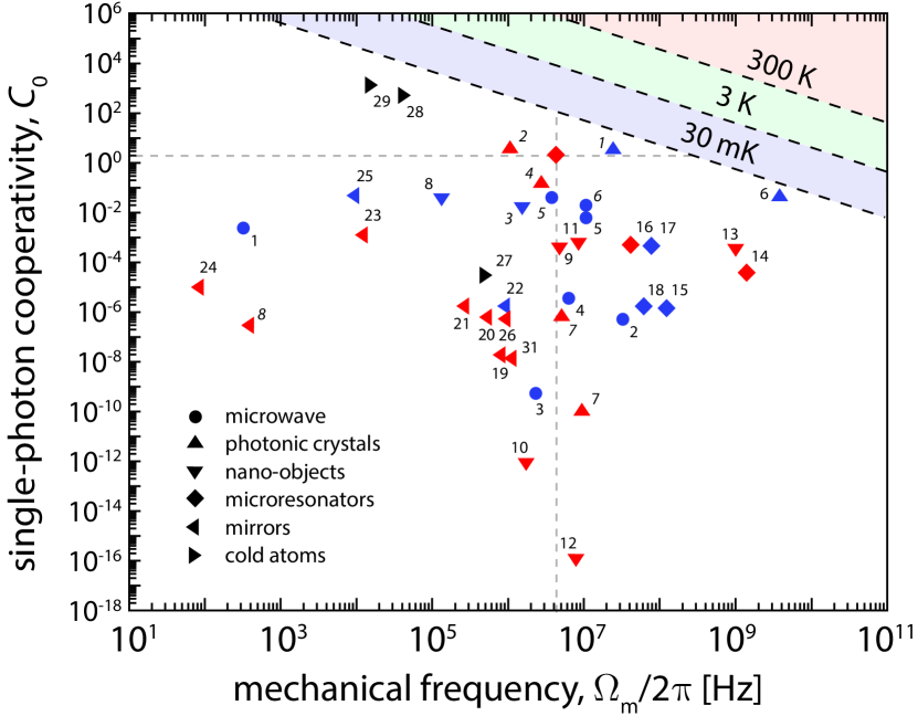
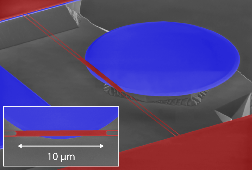
A typical device is shown in Fig. 1, corresponding to a beam positioned 25 nm above a 0.65-m-thick, 30-m-diameter microdisk. By carefully varying the dimensions of the beam, the disk, and their lateral offset with respect to this nominal geometry, we achieve optomechanical coupling rates () in excess of GHz/nm while maintaining cavity decay rates () as low as MHz and radio frequency ( MHz) flexural beam modes with damping rates () as low as Hz. In conjunction with the small mass ( pg) and large zero-point displacement ( fm) of the beam modes, the combined low-loss, small gap and parallel-plane geometry result in a vacuum optomechanical coupling rates () as high as kHz and room temperature single-photon cooperativities as high as . The latter is notably a factor of times larger than in Gavartin et al. (2012) and on par with the state-of-the-art for both room temperature and cryogenic COMS (Fig. 2).
In conjunction with high , several features of the system make it well-suited for quantum-limited operation. First, SiO2 microcavities with the reported dimensions and internal loss readily support intracavity photon numbers of . This enables quantum cooperativities () approaching unity — a basic requirement for performing a Heisenberg-limited displacement measurement — for a room temperature thermal occupation of , corresponding to MHz. Another striking feature is the exceptionally large magnitude of the cavity frequency noise produced by zero-point motion of the mechanical oscillator, . This magnitude is many orders of magnitude larger than typical extraneous sources of noise due to laser frequency fluctuations or TRN Anetsberger et al. (2010). Taking advantage of these strengths, recent deployment of the device in a 4 K Helium cryostat enabled interferometric measurements with a read-out noise 43 dB below (corresponding to an imprecision 40 dB below that necessary to reach the SQL) and with an imprecision-back-action product of , allowing active feedback cooling to near the motional ground state Wilson et al. (2015). Below, we demonstrate a measurement with an imprecision 30 dB below that at the SQL and an imprecision-back-action product of , using a moderate input power of 10 W. Remarkably, the imprecision due to microdisk TRN Anetsberger et al. (2010) can be dB lower.

In the following sections we carefully detail the design, fabrication, and characterization of the device, and provide a demonstration of low noise displacement measurement. Sec. II gives an overview of nanobeam and microdisk resonators and describes a numerical model used to predict their gradient-force optomechanical coupling. Notably, we find that can be improved by an order of magnitude by carefully positioning the beam above the disk. Sec. III describes the fabrication method, particularly the use of planarized (by CMP) sacrificial layers and e-beam lithography, which enable precise engineering of the vertical and horizontal beam-disk separation, respectively. Sec. IV describes characterization of the device using thermomechanical noise measurements and the optical spring effect. In Sec. V, we discuss an experiment in which the microdisk is embedded into fiber-based homodyne interferometer, enabling displacement read-out with an imprecision 33 dB below for the fundamental beam mode. Finally, in Sec. VI, we remark on the feasibility of Heisenberg-limited position measurements and functionalized applications which take advantage of the heterogeneous integration method.
II Device design
II.1 Nanomechanical beam
The mechanical resonator we study is a doubly-clamped beam released from a high-stress Si3N4 thin film Verbridge et al. (2006). Stressed “nanobeams” are attractive for their string-like flexural modes, which possess exceptionally high ratios Imboden and Mohanty (2014). Beams with of the dimensions studied — — possess effective masses pg, fundamental frequencies MHz and room temperature quality factors Verbridge et al. (2006). Significantly, is well in excess of the “universal” value of observed for bulk amorphous glass resonators at temperatures above K Pohl et al. (2002). It is also higher than for typical unstressed, single-crystal nanobeams due to surface loss Villanueva and Schmid (2014). This exceptional behavior is known to derive from a combination of large impedance mismatch from the anchoring body Rieger et al. (2014) (suppressing extrinsic loss) and stress-related “dilution” of intrinsic loss González and Saulson (1994); Unterreithmeier et al. (2010); Villanueva and Schmid (2014). From the standpoint of quantum-limited measurement, an important consequence of their high is that high-stress nanobeams exhibit large zero-point fluctuations. Expressed as a single-sided spectral density evaluated at the mechanical frequency, the above parameters correspond to a peak zero-point displacement noise density of . This value occurs in a radio frequency window, 1-10 MHz, where low noise electronics and laser sources are available; as such, nanobeams were the first solid state mechanical resonators to be read out electrically (using a metal beam) Teufel et al. (2009) and optically Anetsberger et al. (2010) with an imprecision lower than .
Measurements of for a typical disk-integrated beam with dimensions are shown in Fig. 3. Despite the complexity of the fabrication procedure (Sec. III), flexural modes exhibit as high as Hz, on par with the state-of-the-art for high-stress Si3N4 nanobeams of similar dimensions Verbridge et al. (2008); Villanueva and Schmid (2014). The near-linear eigenfrequency spectrum, , is consistent with a tensile stress of MPa assuming a density of Verbridge et al. (2006). The mechanical-Q spectrum, , is consistent with the intrinsic loss model of Unterreithmeier et al. (2010); Villanueva and Schmid (2014). The dashed line in Fig. 3 is a fit to this model: , where , is the elastic modulus of the film, and is the intrinsic quality factor of the film when unstressed. The inferred value of (using GPa), is roughly an order of magnitude lower than that for bulk Si3N4. Interpreted as surface loss, however, the inferred coefficient of is within a factor of two of the typical value for LPCVD SiN thin films Villanueva and Schmid (2014). Operating in a 3He cryostat at 0.5 K, we have recently observed Ghadimi and Schilling (2015).
In addition to its favorable mechanical properties when stressed, Si3N4 is an attractive optical material. It has a relatively large index of refraction, , and, owing to its eV bandgap, respectably low optical absorption at near infrared wavelengths, characterized by an imaginary index of Zwickl et al. (2008).
II.2 Optical microdisk
The optical resonator we employ is a SiO2 microdisk supporting WGMs along its periphery. SiO2 microdisks possess several advantages for evanescent sensing. The first advantage is that SiO2 exhibits a wide transparency window and a large power handling capacity, enabling large intracavity photon numbers (). The practically achievable is typically limited by Kerr and Raman nonlinearity. At visible and telecommuncation wavelengths, other effects such as multi-photon absorption do not play a significant role in SiO2, in contrast to Si and other semiconductors. A second advantage is that standard lithographic techniques, in conjunction with wet-etching, can produce SiO2 microdisks with exceptionally high (recently exceeding in the telecommunication band Lee et al. (2012)). This feature is related to the wedged rim of the disk, which supports WGMs that are spatially isolated from the surface, and thereby from surface scattering/absorption loss. A third advantage is that microdisk WGMs can be evanescently coupled to tapered optical fibers with high ideality Spillane et al. (2003). This feature is critical for sensing applications, in which optical loss produces elevated shot-noise imprecision Schliesser et al. (2008).
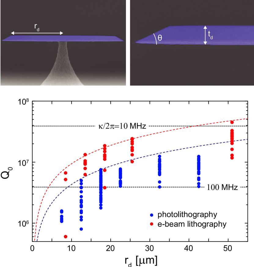
Microdisk resonators were in this case studied at nm (outside of the telecommunications window), to allow for smaller optical mode volumes. As discussed in Sec. II.3, reducing the disk radius () and thickness () results in smaller mode volumes with fractionally larger evanescent components, thereby increasing the optomechanical coupling strength. Fig. 4 shows measurements (see Sec. IV.1 for details) of optical versus disk radius () for microdisk samples of thickness . Two sets of devices are considered. The first set was prepared with photolithography, the second with electron-beam lithography. The sets differ by their corresponding wedge angle, which is 30 (11) degrees for wet (e-beam) lithography. For both disk preparation methods, intrinsic was measured for radii as low as , corresponding to loss rates of MHz. For shallower wedge angles, as high as (MHz) was obtained — notably exceeding (for the same ) those measured at telecom wavelengths, where scattering losses are significantly lower Kippenberg et al. (2006); Lee et al. (2012). Numerical simulations Oxborrow (2007) reveal that radiation contributes negligibly to the measured loss. Dotted blue (red) lines in Fig. 4 are guide-to-the-eye models for , consistent with loss due to surface absorption/scattering Borselli et al. (2005), and corresponding to a fixed finesse of . As discussed in Sec. IV.4, the intrinsic microdisk is ultimately reduced by loss introduced by the nanobeam, for beam-disk separations of less than 100 nm.
II.3 Evanescent optomechanical coupling
Optomechanical coupling is achieved by placing the nanobeam near the surface of the microdisk, so that its mid-section occupies the evanescent volume of one of the microdisk WGMs. When the WGM is excited, the beam experiences a gradient force, . The magnitude of this force, and likewise the optomechanical coupling factor , can be derived by computing the work done on the WGM, , by a small displacement of the beam, : that is, , where is the potential energy stored in the cavity field Povinelli et al. (2005); Van Thourhout and Roels (2010). To first order, it can be shown that Anetsberger et al. (2009)
| (1a) | ||||
| (1b) | ||||
where is the local relative permittivity, is the unperturbed cavity field amplitude, and indicates an integral over the volume occupied by the beam (disk). The simplified expression in Eq. 1b replaces with an index of refraction and parameterizes each integral in terms of the intensity-weighted volume of the beam (disk), , where is the maximum of the unperturbed field within the beam (disk).
To gain physical insight into Eq. 1, we consider the configuration shown in Fig. 5. Here the beam is placed above the disk, so that it samples the vertical evanescence of a WGM. For simplicity, the transverse dimensions of the beam are assumed to be much smaller than that of the evanescent field; that is, and , where is the effective cross-sectional area of the WGM and is the exponential decay length of the evanescent field. In this case can be approximated as , where is the intensity-weighted “sampling length” of the beam. Likewise can be parameterized as , where is the physical disk radius. Assuming the form , neglecting the weak position dependence of , and assuming the effective mass of a point probe, , the vacuum optomechanical coupling rate can be approximated as
| (2) |
where is the mass density of the beam. In practice and must be determined numerically for a wedged microdisk. An estimate can be made, however, by assuming the mode shape of a microtoroid WGM with a minor radius of Anetsberger et al. (2009). In this case, using , one has , and Anetsberger (2010). Using these formulas, the device geometry , and assuming nm, , kg/m3, MHz, and m (see Sec. IV.6), Eq. 2 predicts that GHz/nm, fm, and kHz. As shown in Fig. 5d, this estimate agrees well with numerically and experimentally determined values. Notably, Eq. 2 implies that to achieve large , it is necessary to reduce the vertical gap to nm, and to maximize by laterally positioning the beam above the disk.
A numerical model for is shown in Fig. 5b. Intrinsic WGM mode shapes, , were computed using an axially-symmetric finite element model (COMSOL FEM axial symmetric package Oxborrow (2007)). The energy stored in the WGM, , and the energy shift due to the beam, , were computed by numerical integration in Matlab. Differentiating the 2D energy landscape gives for out-plane-motion. Fig. 5b shows for a beam and disk with the dimensions given above, for a TM-like WGM mode. Contours indicate that the optimal position of the beam is above and inside the inner rim of the disk, and that the magnitude of scales exponentially with vertical displacement from the disk surface, with a decay length of nm. A horizontal cut through the contours for nm is shown in Fig. 5c. Upper and lower curves show models for fundamental in-plane (IP) and out-of-plane (OP) flexural modes. Significantly, maximizing also minimizes ; this opens a wide spectral window, , for measurement of the out-of-plane mode. Experimental measurements (see Sec. IV.2) of are also shown in Fig. 5c . The model agrees well with experiment assuming a vertical offset of nm.
III Device fabrication
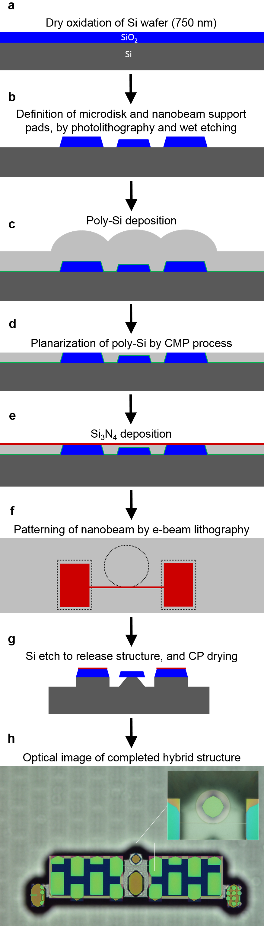
The fabrication process is outlined in Fig. 6. Four key elements of the process, detailed in the following subsections, are: (A) fabrication of the SiO2 microdisk, (B) formation of a planarized sacrificial layer using chemical mechanical polishing (CMP), (C) fabrication of the Si3N4 nanobeam, and (D) release of the sacrificial layer. Of particular importance is the sacrificial layer, which allows the mechanical (Si3N4) and optical (SiO2) elements to be designed independently while maintaining the high optical quality and achieving a vertical beam-disk separation of less than 100 nm. Also important is the use of e-beam lithography to pattern the Si3N4, as this enables fine tuning of the lateral beam position.
III.1 Microdisk fabrication
The process begins with an undoped, float-zone (FZ) Si wafer, on which a 750 nm film of SiO2 is grown by dry oxidation. Three structures are patterned into the SiO2 film: the microdisk, rectangular pads that later serve as a support for the nanobeam and a reference plane for CMP polishing, and markers that are later used for e-beam alignment. As illustrated in Fig. 7, the SiO2 pattern is processed in two stages. In the first stage all structures are defined. In the second stage the microdisk is etched preferentially, recessing it from the pads and defining the vertical gap between disk and the beam.
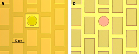
Details of the SiO2 patterning process are as follows: The first mask, containing all structures, is exposed in of Microchemicals AZ 1512 photoresist using a Karl Süss MA 150 mask aligner and a broadband Hg lamp. A subsequent reflow step is used to smooth the pattern boundaries and minimize standing wave patterns. Afterwards, the pattern is transfered to SiO2 by etching in a room-temperature bath of BHF. The photoresist is then stripped and a second mask is applied. The second mask covers all structures on the wafer except for the microdisk, leaving it exposed for etching (Fig. 7a). The microdisk is preferentially etched in BHF until it is 10-100 nm thinner than the surrounding pads (later defining the beam-disk gap). The result, after the photoresist is stripped, is shown in Fig. 7b. Note that the microdisk reflects a different color than the surrounding pads due to its reduced thickness. Also seen in Fig. 7 is a matrix of sacrificial pads surrounding the disk. This matrix extends across the entire wafer and is only broken where microdisks or alignment marks (not shown) are placed. As discussed in Sec. III.2, a uniform matrix of pads is necessary to achieve a flat surface when performing CMP the sacrificial layer.
The final result of microdisk fabrication is illustrated in Fig. 6b. Blue indicates (in profile) the patterned SiO2 film, with the microdisk in the center and nanobeam support pads on either side. Not shown are sacrificial pillars and alignment marks. In the next processing step, all structures are buried in a sacrificial material, onto which a Si3N4 film will be grown.
III.2 Planarized sacrificial layer
After patterning, the SiO2 film is covered with a layer of sacrificial material. The sacrificial layer is used as a substrate for deposition and patterning of the Si3N4 film, meanwhile protecting the underlying microdisk. A crucial consideration is the thickness and flatness of the sacrifical layer, which is initially uneven because of its conformity to the underlying SiO2 pattern. To thin and planarize the sacrificial layer, a delicate chemical-mechanical polishing (CMP) procedure is followed.
Poly-Si is chosen as the sacrificial material because it can be isotropically etched with high selectivity to SiO2 and Si3N4, is well-suited to CMP, can withstand the high temperatures required for LPCVD Si3N4 (), and can be used to undercut the nanobeam and the microdisk in a single step. A 1.5 m thick layer is deposited by LPCVD at using silane and disilane as reactants. In addition, immediately before poly-Si deposition, a 5 nm aluminum oxide (Al2O3) film is deposited atop the SiO2 using atomic layer deposition. This film later serves as an etch-stop to protect the microdisk when releasing the Si3N4 nanobeam. (Al2O3 etches over slower than Si3N4 in flourine-based RIE used, and thus a few nanometers is sufficient to protect the microdisk.)
A profile of the per-polished sacrificial layer is sketched in Fig. 6c. The Al2O3 etch-stop film is indicated by green. Immediately above the etch-stop is the layer of poly-Si (gray). Because of the underlying SiO2 structures, the surface of the poly-Si is uneven. This surface is planarized by CMP before Si3N4 is deposited.
CMP involves pressing the wafer against a rotating polishing pad in the presence of an abrasive and corrosive chemical slurry. Abrasion is provided by SiO2 particles 30-50 nm in diameter. The slurry PH is adjusted to achieve the desired polishing rate. In practice the polishing rate is also a function of applied force, rotation speed, and wafer topography. Areas of the wafer where features are sparse experience a higher pressure and thus a higher polishing rate than areas where features are dense. In order to reduce the poly-Si thickness to less than 100 nm over the entire 100 mm wafer, a uniform polishing rate is critical. This is the reason for patterning a matrix of sacrificial pads (Fig. 7).
The objective of the CMP process is to remove poly-Si until the pads are exposed, while maintaining a thin layer above the recessed microdisk (Fig. 6d). This procedure is complicated by the fact that the polishing rate varies across the wafer and, more importantly, that the polishing rate above the microdisk is faster than the rate above the adjacent nanobeam support pads. The latter results in a poly-Si layer which is thinner above the microdisk than at the nanobeam supports. To reduce this “dishing” effect, the support pads are brought as close the microdisk as possible (limited to by photolithography and BHF biasing). To further reduce dishing, a two step polishing technique is used. First a slurry designed to etch poly-Si is used to remove the bulk of the material, leaving approximately 100 nm above the pads. The remaining material is removed with a slurry designed to etch SiO2 faster than poly-Si. When the surface of the SiO2 pads is reached, the dishing effect begins to reverse, resulting in an overall flat surface.
The gap between the microdisk and nanobeam is not determined by the thickness of the sacrificial layer, but rather by the predefined difference in thickness between the microdisk and the pads (Fig. 6b). During the final steps of CMP, however, the support pads are etched. The final gap is therefore smaller than originally defined by thinning of the microdisk. In order to precisely tune the gap, the thickness of the clamping pads is iteratively measured by reflectometry until a desired value is reached. The sample is then ready for Si3N4 deposition.
III.3 Nanobeam fabrication
To form the nanobeam, a 50-100 nm film of high-stress Si3N4 is deposited onto the planarized poly-Si layer. LPCVD is performed at using dichlorosilane and ammonia, producing a nearly stoichiometric Si3N4. High stoichiometry is important for reducing absorption caused by hydrogen and oxygen impurities Zwickl et al. (2008). Moreover, the stress (800 MPa) resulting from high temperature deposition is important for achieving high mechanical quality factors Verbridge et al. (2006).
To maximize optomechanical coupling, it is necessary to fine tune the lateral beam-disk separation with nm precision (Fig. 5c). This is accomplished using e-beam lithography to define the beams, in conjunction with the alignment markers defined during SiO2 patterning. Importantly, after Si3N4 deposition, the markers are buried under Si3N4 and poly-Si, and cannot be seen by the electron-beam. A series of etch steps are used to locally uncover the markers; in addition, to improve contrast, the exposed markers are used as a hard mask to etch into the underlying Si, using a highly selective flourine-based etch. The resulting high-contrast markers permit alignment of the Si3N4 mask with sub-100 nm precision.
The nanobeams, support pads, and sample labels are patterned in a 180 nm-thick hydrogen silsesquioxane (HSQ) negative photoresist. To reduce writing time, the pattern is separated into two parts, one containing the nanobeams and one containing the pads and labels. The former is written with a high resolution of 5 nm, while the latter is written with a 50 nm resolution. Proximity effect correction is used to ensure a high fidelity pattern. The e-beam pattern is transferred to Si3N4 using an SF6 RIE etch. The resulting structure is shown in Fig. 8a.

III.4 Structural release
III.4.1 Mesa and sample chip
Before the nanobeam and microdisk are released, they are elevated from the surrounding wafer on a rectangular “mesa”. This later enables alignment of a straight tapered optical fiber to the microdisk Riviere et al. (2013). Figure 8b shows the mesa defined in a mask of Microchemicals AZ 9260 photoresist. Flourine-based RIE is used to remove the surrounding poly-Si. The underlying sacrificial SiO2 pads are removed by a subsequent BHF etch, exposing the Si substrate. To create the elevated mesa, exposed Si is recessed an additional by DRIE.
After releasing the mesa, the sample chips are defined. To define the sample chips, the wafer is coated with a protective photoresist layer and partially diced ( deep) with a high precision Si dicing saw. Partial dicing is important as it leaves the wafer intact, enabling further processing using wafer-scale equipment. After partial dicing the photoresist is stripped, so that final release steps can be carried out.
III.4.2 Nanobeam and microdisk
To release the nanobeam and undercut the microdisk, the partially diced wafer is immersed in KOH at , selectively removing poly-Si but also etching Si. The etch time is fine-tuned with two opposing criteria in mind: (1) to ensure that the microdisk is undercut sufficiently far from its rim to avoid optical losses and (2) to ensure that Si underneath the nanobeam clamping point is not etched away. After KOH etching, the wafer is rinsed in water and any remaining potassium is neutralized in a bath of hydrochloric acid. Organic cleaning is then performed using an exothermic mixture of three parts sulfuric acid to one part 30% hydrogen peroxide (a “piranha etch”). After rinsing again, the wafer is transfered directly to the ethanol bath of a critical point drying (CPD) machine. After CPD, the wafer is broken into sample chips along the partially diced lines, concluding the fabrication process.
IV Device characterization
IV.1 Experimental setup
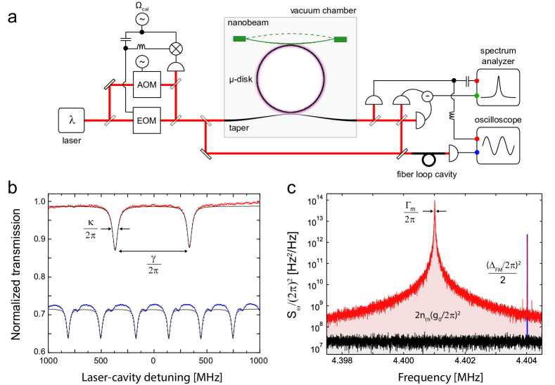
Samples are characterized using the experimental setup shown in Fig. 9. Light from a nm tunable diode laser (New Focus Velocity 6312) is coupled into the microdisk using a tapered optical fiber (780 HP) Spillane et al. (2003). The forward-scattered (“transmitted”) field is monitored using one of two techniques: direct detection with an avalanche photodiode (Thorlabs APD110) and balanced homodyne detection with a pair of fast Si photodiodes (FEMTO HCA-S-100). DC- and AC-filtered photosignals are split between an oscilloscope (Tektronix DPO4034) and a spectrum analyzer (Tektronix RSA5106A). To calibrate laser-cavity detuning, a fraction of the input field is simultaneously passed through a -cm-long (FSR MHz) fiber loop cavity. Optical decay rates are inferred from measurements of transmitted power versus laser detuning (Fig. 9b). Mechanical properties, including the optomechanical coupling rates, are inferred from measurements of thermomechanical cavity frequency noise Gorodetsky et al. (2010) (Fig. 9c). To calibrate this noise, the input field is frequency modulated using an electro-optic modulator (EOSpace). Residual amplitude modulation — an important source of calibration error — is actively suppressed by stabilizing the phase of an out-of-loop heterodyne beat Zhang et al. (2014). To eliminate gas damping of the nanobeam, the sample chip and the fiber coupling setup (based on an Attocube stack) are embedded in a vacuum chamber operating at mbar.
IV.2 Thermal noise measurement
Mechanical mode frequencies , damping rates , and optomechanical coupling rates , were determined by analyzing the cavity resonance frequency noise produced by thermal motion of the nanobeam. An in-depth description of this method is given in Gorodetsky et al. (2010). Important details are recounted below for clarity.
Thermal motion of the nanobeam is written onto the cavity resonance frequency via their optomechanical coupling, . To measure , we monitor the power of the transmitted field while operating at a fixed detuning of . Referred to the output voltage () of the photodetector transimpedance amplifier, the uncalibrated noise spectrum can be expressed as , where is the measurement transfer function and is the apparent cavity frequency noise. is calibrated by applying a phase modulation tone of known depth () and frequency () to the input, resulting in a narrow spectral peak with area Gorodetsky et al. (2010).
A representative measurement is shown in Fig. 9c. Red, blue, and black components correspond to thermal noise, , the calibration tone, , and measurement imprecision, , respectively. The full signal can be modeled as
| (3a) | ||||
| (3b) | ||||
| (3c) | ||||
where is a normalized Lorentzian (characterizing the mechanical susceptibility) and is a normalized Gaussian (characterizing the window function of the spectrum analyzer, which is assumed to have a resolution bandwidth ). To calibrate the vertical axis in Fig. 9c, it is assumed that . Fitting the calibrated spectrum to Eq. 3 gives , , and . The last inference requires knowledge of . By using input powers low enough to neglect photothermal/radiation pressure damping ( nW), we assume that .
IV.3 Optical spring effect
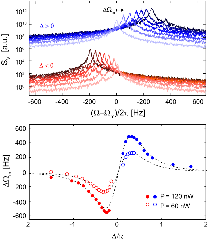
As a cross-check of the thermal noise measurement, was independently estimated from the optical spring effect Aspelmeyer et al. (2014). In the experimentally relevant bad cavity limit (), the mechanical frequency shift produced by a radiation pressure optical spring is
| (4) |
where is the laser-cavity detuning, is the intracavity photon number, and is the power injected into the cavity. (We note that radiation pressure damping also occurs for a detuned input field; however, in the devices studied, for which , this effect was found to be overwhelmed by photothermal damping Metzger and Karrai (2004).)
A measurement of the optical spring effect is shown in Fig. 10, corresponding to the sample also characterized in Fig. 9c. The injected powers used — nW — were chosen to avoid instabilities due to photothermal/radiation pressure damping. The cavity was critically coupled ( MHz) and laser detuning was estimated from the mean transmitted power. Overlaid models correspond to Eq. 4 with the value kHz, inferred from a least-squared fit to the low power measurement. This value is within 10 of that inferred from thermal noise in Fig. 9c.
IV.4 and versus lateral beam position
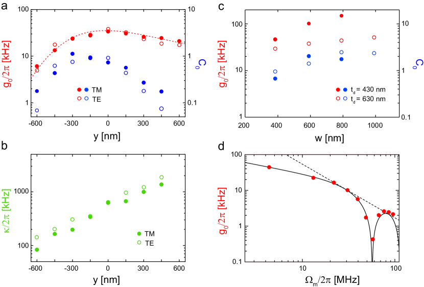
As discussed in Sec. II.3, depends sensitively on the lateral positioning of the nanobeam, and assumes a maximum (minimum) value for out-of-plane (in-plane) flexural modes when centered above the WGM. This behavior was studied by sweeping the lateral position of the beam using an appropriate e-beam mask (Sec. III.3). Measurements of versus lateral beam position are shown in Fig. 11a. (In-plane modes exhibit typically lower , and were not considered.) for beam and disk dimensions of m and , respectively, and for a vertical gap of 25 nm. In agreement with numerical modeling (dashed line), assumes a maximum of kHz as the outer edge of the beam eclipses the rim of the disk.
Also shown in Fig. 11b are measurements of versus lateral beam position (). When the beam is displaced far from the disk, converges to the intrinsic value of MHz observed in Fig. 4, suggesting that CMP did not significantly affect microdisk surface quality. As the beam is brought within 100 nm of the disk, is observed to increase sharply. The observed exponential dependence on is independent of mode polarization and similar to the scaling observed in Anetsberger et al. (2010) with a beam coupled to a microtoroid. The absolute magnitude of the loss is also inconsistent with bulk Si3N4 optical absorption — specifically, accounting for the relatively small fraction of energy stored in the beam, the observed loss would require an imaginary index of , which is 1-2 orders of magnitude larger than conventionally observed for Si3N4 at NIR wavelengths Zwickl et al. (2008); Wilson et al. (2009). We thus conjecture that this loss is due to scattering from and/or waveguide coupling into the beam.
Combining measurements of and with typical room temperature mechanical damping rate of Hz (we observed no change in for small beam-disk seperation, suggesting that squeeze-film gas damping Verbridge et al. (2008) was not a factor), the single-photon cooperativity is observed to approach . This value is limited by the unfavorable scaling of as begins to saturate. Despite this limitation, the inferred represents a nearly 50 dB increase over our prior chip-scale implementation Gavartin et al. (2012), owing to the combined 100-fold increase of and 10-fold reduction in . Increase is due to the precise vertical and lateral positioning of the beam afforded by CMP and e-beam processing. Reduced is due to greater isolation of the disk during beam patterning, making use of the poly-Si sacrificial layer. Fig. 11b suggests that is ultimately dominated by beam-induced scattering/absorption loss, rather than deterioration of intrinsic disk loss (Fig. 4), implying that an additional 10-fold reduction in may yet be realized with appropriate beam shaping/positioning.
IV.5 and versus beam width and disk thickness
Wider beams () and thinner disks were fabricated in an attempt to increase and (see Eq. 2). Measurements of vs for two microdisk thicknesses, , are shown in Fig. 11. Fixed dimensions of the nanobeam and microdisk are and , respectively. The lateral beam position was chosen to maximize for the -wide beam (see Fig. 11). For the TE optical modes studied, a roughly 2 increase in was observed for the thinner disk. In both cases, scaled roughly linearly for widths m. also increased with , roughly in proportion to , for both . This is due to the fact that (not shown) was roughly independent of for both disk thicknesses and a factor of four larger for the thinner disk. The highest optomechanical coupling rate we have measured, kHz, was for a 1 m-wide beam coupled to a -thick disk. The highest cooperativities observed, , were for 1 m-wide beams coupled to disks of both thicknesses.
IV.6 versus mechanical mode order
was also studied for higher order mechanical modes. As shown in Fig. 11d , decreases as the vibrational node spacing approaches the dimensions of the effective sampling length . In this case the model in Sec. II.3 — which assumes rigid displacement of a beam with effective mass — breaks down. A simple extension of the model is shown as a red line in Fig. 11d. Here is computed with respect to optical-intensity-weighted displacement of the mechanical mode:
| (5a) | ||||
| (5b) | ||||
where is the displacement profile of the -order out-of-plane flexural mode. The latter expression is appropriate when the transverse dimensions of the beam are much smaller than that of the WGM, and assumes that the intensity distribution sampled by the beam is uniform along the beam axis with an effective sampling length . Using gives for odd and 0 for even . The model shown in Fig. 11d agrees quantitatively with experiment assuming an effective length of m as the only free parameter. A simple route to increasing would be to remove mass from the beam outside of the effective sampling length (see Fig. 13).
V Displacement sensitivity
As an illustration of device performance, we use the microdisk to perform a cavity-enhanced interferometric measurement of the beam’s displacement. For this purpose, the fiber taper and microdisk are embedded in one arm of a length- and power-balanced homodyne interferometer (Fig. 9). The cavity is driven on resonance using the Pound-Drever-Hall technique. A piezoelectric mirror is use to stabilize the interferometer path length difference so that the homodyne photocurrent is proportional to the phase of the transmitted cavity field.
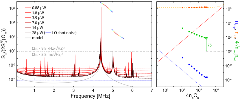
Displacement noise spectra are shown in Fig. 12 for a m beam with optomechanical parameters . (Here corresponds to the critically-coupled cavity linewidth and other parameters correspond to the fundamental out-of-plane mechanical mode.) For the measurements shown, the cavity was critically coupled and the power of the input field was swept from W. The homodyne photocurrent noise spectrum is plotted in units relative to the signal produced by a phonon of displacement (equivalent to assuming fm). In these units, the magnitude of the fundamental thermal noise peak (neglecting photothermal or dynamical back-action) is equal to the effective thermal occupation , where is the ambient bath occupation, is the effective thermal bath occupation associated with classical and quantum measurement back-action, and is the apparent thermal occupation associated with the measurement imprecision, . The noise spectra are calibrated by bootstrapping a low power measurement to . For larger optical powers, dynamic spring/damping forces modify the peak. At the highest optical powers, the displacement imprecision in the vicinity of is estimated (from the saddle at 2.5 MHz) to be , while the shot-noise equivalent displacement is . These correspond to imprecisions 30 and 34 dB below that at the SQL (), respectively. The absolute magnitude of the extraneous imprecision, , is consistent with a mixture of ECDL noise ( Wilson et al. (2015)), TRN ( Anetsberger et al. (2009)), and off-resonant thermal noise (). The latter is estimated using the ‘structural damping’ model of Saulson Saulson (1990),
| (6) |
shown in gray in Fig. 12, for .
The total efficiency of the measurement is estimated by comparing the power dependence of the imprecision (), the effective thermal bath occupation (), and their geometric mean to the ideal values , , and , respectively, where the last case represents the Heisenberg uncertainty limit Wilson et al. (2015). As shown on the right hand side of Fig. 12, the imprecision is a factor of 40 larger than ideal, due to a combination of cavity loss (), taper loss (), homodyne detector loss/misalignment, and optical mode splitting Wilson et al. (2015). The effective thermal bath occupation is inferred by fitting to the off-resonant tail of the fundamental noise peak (to avoid the systematic error due to optical damping). From these fits we infer a heating of , two times larger than expected due to quantum measurement back-action. The imprecision-back-action product is constrained, at high powers, to , due to the saturation of the measurement imprecision. To the best of our knowledge, this represents the closest approach to the uncertainty limit for a room temperature mechanical oscillator.
VI Summary and outlook
We have presented a method to heterogeneously integrate a high-stress, Si3N4 nanobeam within the evanescent near-field of a SiO2 microdisk. Building on earlier strategies Anetsberger et al. (2009); Gavartin et al. (2012), the principle advance is a novel vertical integration technique which preserves the high (mode volume) ratio of each resonator while enabling the beam and the disk to be separated by as little as 25 nm — significantly smaller than the evanescent decay length of the microdisk’s WGMs. Samples of various dimensions were fabricated and characterized. Simultaneously low mechanical loss, , low optical loss, , and large optomechanical coupling rates, , were measured, corresponding to room temperature single-photon cooperativities as high as .
The reported system holds particular promise as a quantum-limited displacement sensor, owing to the large vacuum displacement of the nanobeam and the high power handling capacity of the microdisk. For a typical device, possessing , the resonant vacuum displacement noise, , is orders of magnitude larger than major sources of imprecision — such as laser frequency and thermorefractive noise Anetsberger et al. (2010) — and commensurate with shot noise for an ultra-low intracavity photon number of Wilson et al. (2015). Operating a similar device at 4 K with (corresponding to when critically coupled to the fiber waveguide), we were able to achieve a displacement imprecision times (43 dB) below , while maintaining an imprecision-back-action product within a factor of 5 of the uncertainty limit Wilson et al. (2015). This regime of ‘efficient’ measurement — characterized by the ability to resolve a phonon-equivalent displacement in the thermal decoherence time — enabled us to feedback cool the mechanical mode to near its ground state Wilson et al. (2015), and might be extended to other quantum control tasks, such as squeezed-state preparation Szorkovszky et al. (2011).
An intriguing question is whether the reported device may be used to realize Heisenberg-limited displacement measurements at room temperature. For the radio frequency oscillators under study (), the main challenges are (1) pumping the cavity with photons in order to achieve the necessary measurement strength (characterized by a phonon-equivalent radiation pressure shot noise of ), (2) reducing extraneous sources of measurement imprecision to , and (3) reducing extraneous heating to below . Because of the (blue-stable) thermal self-locking effect in room temperature SiO2 microcavities Arcizet et al. (2009), the first requirement is expected to be limited by parametric radiation pressure instabilities, requiring active feedback damping. (Taking a different approach, cross-correlation techniques may be employed to detect radiation pressure shot noise at the 1 level Verlot et al. (2009), significantly relaxing associated demands on input power and active stabilization.) For microdisks with dimensions studied here, the second requirement is expected to be limited by thermorefractive noise at the level of Anetsberger et al. (2010), an impressive 60 dB lower than . Reaching would require a moderate increase in (for instance, by using lower-mass, “tethered” beams Krause et al. (2015); see Fig. 13). The third requirement depends on the details of the nanoscale heat transfer process. At 4 K, we have observed photothermal heating consistent with an extraneous cooperativity of Wilson et al. (2015); we anticipate this heating to reduce to tenable levels () at room temperature, provided that the underlying process is related to the temperature-dependent thermal conductivity of amorphous glass Pohl et al. (2002). Preliminary room temperature measurements, discussed in Sec. V, suggest that can be met for a moderate .
In addition to high cooperativity, the evanescent sensing platform and reported fabrication method have as a compelling feature the ability to incorporate new materials and/or planar geometries above a high-Q microdisk with nanometric precision. This capability opens the door to a variety of “hybrid” sensing applications. For example, the system may be electrically functionalized by vertically integrating the beam into a parallel plate capacitor, or into the gradient field between two closely spaced electrodes Unterreithmeier et al. (2009); Okamoto et al. (2015). This interface — which need not compromise the mechanical quality of the beam Yu et al. (2012) — can form the basic building block of a high-efficiency electro-optic converter, with applications such as precision radio wave sensing Bagci et al. (2014). Pushed to a different extreme, two dimensional materials such as graphene or MoS2 may be integrated with a microdisk by using the SiN film as a sacrificial substrate Schmid et al. (2014). Another intriguing possibility, in conjunction with the preparation of low entropy mechanical states using measurement-based feedback, is to functionalize the beam with a two-level system, such as an NV center embedded in a diamond nanocrystal Arcizet et al. (2011). Nanobeams integrated with microdisks may also serve as a platform for remotely-coupled “atom-optomechanics” Hammerer et al. (2009); Jöckel et al. (2014), taking advantage of the low oscillator mass, high cavity finesse, and recent developments in fiber-based atom traps Vetsch et al. (2010). Finally, we note that the ability to perform broadband, thermal-noise-limited measurements of high- nanomechanical oscillators may help shed light on the microscopic origin of intrinsic damping Groeblacher et al. (2015).
ACKNOWLEDGMENTS
We acknowledge fabrication advice from E. Gavartin in early stages of the project. All samples were fabricated at the CMi (Center of MicroNanotechnology) at EPFL. Research was funded by an ERC Advanced Grant (QuREM), by the DARPA/MTO ORCHID program, the Marie Curie Initial Training Network ‘Cavity Quantum Optomechanics’ (cQOM), the Swiss National Science Foundation and through support from the NCCR of Quantum Engineering (QSIT). D.J.W. acknowledges support from the European Commission through a Marie Skłodowska-Curie Fellowship (IIF project 331985).
References
- Ekinci and Roukes (2005) K. Ekinci and M. Roukes, Rev. Sci. Instru. 76, 061101 (2005).
- Cleland and Roukes (1998) A. N. Cleland and M. L. Roukes, Nature 392, 160 (1998).
- Mamin and Rugar (2001) H. Mamin and D. Rugar, App. Phys. Lett. 79, 3358 (2001).
- Jensen et al. (2008) K. Jensen, K. Kim, and A. Zettl, Nature Nano. 3, 533 (2008).
- Schwab and Roukes (2005) K. C. Schwab and M. L. Roukes, Physics Today 58, 36 (2005).
- LaHaye (2004) M. D. LaHaye, Science 304, 74 (2004).
- Flowers-Jacobs et al. (2007) N. Flowers-Jacobs, D. Schmidt, and K. Lehnert, Phys. Rev. Lett. 98, 096804 (2007).
- Regal et al. (2008) C. A. Regal, J. D. Teufel, and K. W. Lehnert, Nat. Phys. 4, 555 (2008).
- Teufel et al. (2011) J. D. Teufel, D. Li, M. S. Allman, K. Cicak, A. J. Sirois, J. D. Whittaker, and R. W. Simmonds, Nature 471, 204 (2011).
- Kippenberg and Vahala (2008) T. J. Kippenberg and K. J. Vahala, Science 321, 1172 (2008).
- Aspelmeyer et al. (2014) M. Aspelmeyer, T. J. Kippenberg, and F. Marquardt, Rev. Mod. Phys. 86, 1391 (2014).
- Caves (1980) C. M. Caves, Phys. Rev. Lett. 45, 75–79 (1980).
- Chan et al. (2011) J. Chan, T. P. M. Alegre, A. H. Safavi-Naeini, J. T. Hill, A. Krause, S. Groeblacher, M. Aspelmeyer, and O. Painter, Nature 478, 89 (2011).
- Verhagen et al. (2012) E. Verhagen, S. Deléglise, S. Weis, A. Schliesser, and T. J. Kippenberg, Nature 482, 63 (2012).
- Teufel, J. D. et. al. (2011) Teufel, J. D. et. al., Nature 475, 359 (2011).
- Wilson-Rae et al. (2007) I. Wilson-Rae, N. Nooshi, W. Zwerger, and T. J. Kippenberg, Phys. Rev. Lett. 99, 093901 (2007).
- (17) V. B. Braginsky and Braginskiĭ, Quantum measurement.
- Wilson et al. (2015) D. Wilson, V. Sudhir, N. Piro, R. Schilling, A. Ghadimi, and T. Kippenberg, Nature 524, 325 (2015).
- Krause et al. (2015) A. G. Krause, T. D. Blasius, and O. Painter, arXiv preprint arXiv:1506.01249 (2015).
- Purdy et al. (2013a) T. P. Purdy, R. W. Peterson, and C. A. Regal, Science 339, 801 (2013a).
- Teufel et al. (2016) J. Teufel, F. Lecocq, and R. Simmonds, Phys. Rev. Lett. 116, 013602 (2016).
- Courty et al. (2001) J.-M. Courty, A. Heidmann, and M. Pinard, Eur. Phys. J. D 17, 399–408 (2001).
- Szorkovszky et al. (2011) A. Szorkovszky, A. C. Doherty, G. I. Harris, and W. P. Bowen, Phys. Rev. Lett. 107, 213603 (2011).
- Kleckner and Bouwmeester (2006) D. Kleckner and D. Bouwmeester, Nature 444, 75 (2006).
- Thompson et al. (2008) J. D. Thompson, B. M. Zwickl, A. M. Jayich, F. Marquardt, S. M. Girvin, and J. G. E. Harris, Nature 452, 72 (2008).
- Schliesser et al. (2008) A. Schliesser, G. Anetsberger, R. Rivière, O. Arcizet, and T. J. Kippenberg, New J. Phys. 10, 095015 (2008).
- Eichenfield et al. (2009) M. Eichenfield, J. Chan, R. M. Camacho, K. J. Vahala, and O. Painter, Nature 462, 78 (2009).
- Van Thourhout and Roels (2010) D. Van Thourhout and J. Roels, Nat. Phot. 4, 211 (2010).
- Spillane et al. (2003) S. Spillane, T. Kippenberg, O. Painter, and K. Vahala, Phys. Rev. Lett. 91, 043902 (2003).
- Anetsberger et al. (2009) G. Anetsberger, O. Arcizet, Q. P. Unterreithmeier, R. Rivière, A. Schliesser, E. M. Weig, J. P. Kotthaus, and T. J. Kippenberg, Nat. Phys. 5, 909 (2009).
- Doolin et al. (2014) C. Doolin, P. Kim, B. Hauer, A. MacDonald, and J. Davis, New J. Phys. 16, 035001 (2014).
- Cole et al. (2015) R. M. Cole, G. A. Brawley, V. P. Adiga, R. De Alba, J. M. Parpia, B. Ilic, H. G. Craighead, and W. P. Bowen, Phys. Rev. App. 3, 024004 (2015).
- Neuhaus et al. (2012) L. Neuhaus, E. van Brackel, E. Gavartin, P. Verlot, and T. Kippenberg, in CLEO: Science and Innovations (Optical Society of America, 2012) pp. CW3M–2.
- Gavartin et al. (2012) E. Gavartin, P. Verlot, and T. J. Kippenberg, Nat. Nano. 7, 509 (2012).
- Anetsberger et al. (2010) G. Anetsberger, E. Gavartin, O. Arcizet, Q. P. Unterreithmeier, E. M. Weig, M. L. Gorodetsky, J. P. Kotthaus, and T. J. Kippenberg, Phys. Rev. A 82 (2010).
- Norte et al. (2015) R. A. Norte, J. P. Moura, and S. Gröblacher, arXiv preprint arXiv:1511.06235 (2015).
- Safavi-Naeini et al. (2013) A. H. Safavi-Naeini, S. Groeblacher, J. T. Hill, J. Chan, M. Aspelmeyer, and O. Painter, Nature 500, 185 (2013).
- Purdy et al. (2013b) T. P. Purdy, P.-L. Yu, R. W. Peterson, N. S. Kampel, and C. A. Regal, Phys. Rev. X 3 (2013b).
- Leijssen and Verhagen (2015) R. Leijssen and E. Verhagen, arXiv preprint arXiv:1505.00324 (2015).
- Wollman et al. (2015) E. E. Wollman, C. Lei, A. Weinstein, J. Suh, A. Kronwald, F. Marquardt, A. Clerk, and K. Schwab, Science 349, 952 (2015).
- Palomaki et al. (2013) T. Palomaki, J. Harlow, J. Teufel, R. Simmonds, and K. Lehnert, Nature 495, 210 (2013).
- Wu et al. (2014) M. Wu, A. C. Hryciw, C. Healey, D. P. Lake, H. Jayakumar, M. R. Freeman, J. P. Davis, and P. E. Barclay, Phys. Rev. X 4, 021052 (2014).
- Matsumoto et al. (2015) N. Matsumoto, K. Komori, Y. Michimura, G. Hayase, Y. Aso, and K. Tsubono, Phys. Rev. A 92, 033825 (2015).
- Villanueva and Schmid (2014) L. G. Villanueva and S. Schmid, Phys. Rev. Lett. 113, 227201 (2014).
- Verbridge et al. (2006) S. S. Verbridge, J. M. Parpia, R. B. Reichenbach, L. M. Bellan, and H. G. Craighead, J. Appl. Phys. 99, 124304 (2006).
- Imboden and Mohanty (2014) M. Imboden and P. Mohanty, Physics Reports 534, 89 (2014).
- Pohl et al. (2002) R. O. Pohl, X. Liu, and E. Thompson, Rev. Mod. Phys. 74, 991 (2002).
- Rieger et al. (2014) J. Rieger, A. Isacsson, M. J. Seitner, J. P. Kotthaus, and E. M. Weig, Nat. Comm. 5 (2014).
- González and Saulson (1994) G. I. González and P. R. Saulson, J. Acoust. Soc. Am. 96, 207 (1994).
- Unterreithmeier et al. (2010) Q. P. Unterreithmeier, T. Faust, and J. P. Kotthaus, Phys. Rev. Lett. 105, 027205 (2010).
- Teufel et al. (2009) J. D. Teufel, T. Donner, M. A. Castellanos-Beltran, J. W. Harlow, and K. W. Lehnert, Nat. Nano. 4, 820 (2009).
- Verbridge et al. (2008) S. S. Verbridge, R. Ilic, H. Craighead, and J. M. Parpia, App. Phys. Lett. 93, 013101 (2008).
- Ghadimi and Schilling (2015) A. Ghadimi and R. Schilling, in preparation (2015).
- Zwickl et al. (2008) B. M. Zwickl, W. E. Shanks, A. M. Jayich, C. Yang, A. C. Bleszynski Jayich, J. D. Thompson, and J. G. E. Harris, Appl. Phys. Lett. 92, 103125 (2008).
- Lee et al. (2012) H. Lee, T. Chen, J. Li, K. Y. Yang, S. Jeon, O. Painter, and K. J. Vahala, Nat. Phot. 6, 369 (2012).
- Kippenberg et al. (2006) T. Kippenberg, J. Kalkman, A. Polman, and K. Vahala, Phys. Rev. A 74 (2006).
- Oxborrow (2007) M. Oxborrow, in Lasers and Applications in Science and Engineering (International Society for Optics and Photonics, 2007) pp. 64520J–64520J.
- Borselli et al. (2005) M. Borselli, T. Johnson, and O. Painter, Opt. Express 13, 1515 (2005).
- Povinelli et al. (2005) M. L. Povinelli, M. Loncar, M. Ibanescu, E. J. Smythe, S. G. Johnson, F. Capasso, and J. D. Joannopoulos, Opt. Lett. 30, 3042 (2005).
- Anetsberger (2010) G. Anetsberger, Novel cavity optomechanical systems at the micro-and nanoscale and quantum measurements of nanomechanical oscillators, Ph.D. thesis, lmu (2010).
- Riviere et al. (2013) R. Riviere, O. Arcizet, A. Schliesser, and T. J. Kippenberg, Rev. Sci. Instrum. 84, 043108 (2013).
- Gorodetsky et al. (2010) M. L. Gorodetsky, A. Schliesser, G. Anetsberger, S. Deleglise, and T. J. Kippenberg, Opt. Exp. 18, 23236 (2010).
- Zhang et al. (2014) W. Zhang, M. Martin, C. Benko, J. Hall, J. Ye, C. Hagemann, T. Legero, U. Sterr, F. Riehle, G. Cole, et al., Opt. Lett. 39, 1980 (2014).
- Metzger and Karrai (2004) C. H. Metzger and K. Karrai, Nature 432, 1002 (2004).
- Wilson et al. (2009) D. Wilson, C. Regal, S. Papp, and H. Kimble, Phys. Rev. Lett. 103, 207204 (2009).
- Saulson (1990) P. R. Saulson, Phys. Rev. D 42, 2437 (1990).
- Arcizet et al. (2009) O. Arcizet, R. Rivière, A. Schliesser, G. Anetsberger, and T. J. Kippenberg, Phys. Rev. A 80, 021803 (2009).
- Verlot et al. (2009) P. Verlot, A. Tavernarakis, T. Briant, P.-F. Cohadon, and A. Heidmann, Phys. Rev. Lett. 102, 103601 (2009).
- Unterreithmeier et al. (2009) Q. P. Unterreithmeier, E. M. Weig, and J. P. Kotthaus, Nature 458, 1001 (2009).
- Okamoto et al. (2015) H. Okamoto, R. Schilling, H. Shuetz, V. Suhdir, D. J. Wilson, and T. J. Kippenberg, arXiv preprint arXiv:1511.06235 (2015).
- Yu et al. (2012) P.-L. Yu, T. Purdy, and C. Regal, Phys. Rev. Lett. 108, 083603 (2012).
- Bagci et al. (2014) T. Bagci, A. Simonsen, S. Schmid, L. G. Villanueva, E. Zeuthen, J. Appel, J. M. Taylor, A. Sørensen, K. Usami, A. Schliesser, and E. S. Polzik, Nature 507, 81 (2014).
- Schmid et al. (2014) S. Schmid, T. Bagci, E. Zeuthen, J. M. Taylor, P. K. Herring, M. C. Cassidy, C. M. Marcus, L. G. Villanueva, B. Amato, A. Boisen, and E. S. Polzik, J. App. Phys. 115, 054513 (2014).
- Arcizet et al. (2011) O. Arcizet, V. Jacques, A. Siria, P. Poncharal, P. Vincent, and S. Seidelin, Nat. Phys. 7, 879 (2011).
- Hammerer et al. (2009) K. Hammerer, M. Aspelmeyer, E. S. Polzik, and P. Zoller, Phys. Rev. Lett. 102, 020501 (2009).
- Jöckel et al. (2014) A. Jöckel, A. Faber, T. Kampschulte, M. Korppi, M. T. Rakher, and P. Treutlein, Nature Nano. (2014).
- Vetsch et al. (2010) E. Vetsch, D. Reitz, G. Sagué, R. Schmidt, S. Dawkins, and A. Rauschenbeutel, Phys. Rev. Lett. 104, 203603 (2010).
- Groeblacher et al. (2015) S. Groeblacher, A. Trubarov, N. Prigge, G. D. Cole, M. Aspelmeyer, and J. Eisert, Nat. Comm. 6, 7606 (2015).