Cryogenic resonator design for trapped ion experiments in Paul traps
Abstract
Trapping ions in Paul traps requires high radio-frequency voltages, which are generated using resonators. When operating traps in a cryogenic environment, an in-vacuum resonator showing low loss is crucial to limit the thermal load to the cryostat. In this study, we present a guide for the design and production of compact, shielded cryogenic resonators. We produced and characterized three different types of resonators and furthermore demonstrate efficient impedance matching of these resonators at cryogenic temperatures.
1 Introduction
Over the last two decades, the application of ion traps has expanded
from mass spectrometry [1] and frequency
standards [2, 3] towards engineering of
quantum systems which can be used for quantum
computation [4, 5, 6] and
quantum
simulation [7, 8]. It is
commonly accepted that large-scale trapped ion quantum information
processors require micrometer-scale ion traps [5].
Such traps usually suffer from excessive electric field noise close to
metallic surfaces at room temperature, but at cryogenic temperatures
this noise is strongly
reduced [9, 10]. Thus, it seems
natural to move towards cryogenic experimental setups which have the
additional advantage that the ambient pressure is usually a few orders
of magnitude lower than at room temperature. This enables trapping of
longer ion strings due to fewer collisions with background gas.
Furthermore, no bake-out procedure of the vacuum vessel is required,
allowing for rapid trap cycle times.
The operation of Paul traps requires high radio-frequency (RF)
voltages, which are usually generated with the aid of the voltage
gain present in RF resonators. For this purpose, helical resonators
are typically used in the frequency regime up to 50MHz,
whereas for experiments requiring higher drive frequencies coaxial
resonators have been used as
well [11, 12, 13].
In cryogenic experiments, the resonator needs to fulfill different
criteria than in room temperature experiments where the resonator can
be placed outside the vacuum vessel. In particular, the connections in
a cryostat need to have low thermal conductivity to limit the thermal
load. Following the Wiedemann-Franz law, this results in a low
electrical conductivity between room-temperature and the cryogenic
parts of the experiment. Thus, the resonators have to be operated at
the cold-stage. Moreover, space constraints are stricter in cryogenic
systems which makes helical resonators undesirable as they are
generally bulky111Helical resonators have been used in
cryogenic systems [14].. To minimize the
volume of the
resonator, an RLC-series-resonator can be used [15].
In Section 2, we focus on the choice
of the trap drive frequency, the required voltage gain, and voltage
monitoring. Section 3 covers coil design for
three types of coils, and in the following Section 4, we
discuss impedance matching of the resonator and present an efficient
way to match cryogenic resonators. Section 5
focuses on the design of RF shielding, and finally, we present the results
in Section 6.
2 General considerations
In trapped ion experiments, RF-voltages of several hundreds of volts are commonly applied to the trap, which has a simple capacitor as its electrical circuit equivalent. Thus, we need to design a resonator that maximizes the RF-voltage at this capacitor for a given input power. In this section, we discuss general considerations in resonator design which are not limited to a specific resonator type.
2.1 Choosing the trap drive frequency
At first, we consider the losses in an RLC-resonator and its scaling with frequency. From the solution of the equation of motion of a trapped ion in a Paul trap (Mathieu equation), one obtains the trap voltages with the stability parameter [16], which scales as
| (1) |
where is the amplitude of the RF-voltage at the trap and is the trap drive (angular) frequency. Hence, for constant the loss power scales as
| (2) |
A low trap drive frequency will reduce the losses. On the other hand, high secular motion frequencies of the ion in the trap are desirable for operation. Higher secular frequencies require a higher , and thus the desired secular frequencies set a lower limit for . In this study, we aim for a around 0.25, an axial secular frequency of 1MHz, and both radial frequencies to be 3.7MHz. This will require a trap drive frequency of 42.6MHz. Simulations of our trap show that we need a drive voltage of about to reach the desired trap frequencies. In order to limit the thermal load onto the cryostat from dissipated power in the resonator, this voltage should be reached with less than 100mW of RF input power. This power corresponds to a consumption of about 1/7l of liquid helium per hour when operating a wet cryostat at 4.2K [17].
2.2 Voltage gain of an RLC-resonator
Fig. 1 shows an RLC-series-resonator driven through a matching network. In the following, we will assume perfect impedance matching with a loss-less matching network. Thus, we can set the input power equal to the loss power in the resonator , where with being the input voltage supplied to the circuit and the wave impedance of the connecting cable, commonly . We can further write
| (3) |
where is the current in the resonator, its effective loss resistance, its frequency, the voltage at the capacitor, and the capacitor representing the trap. Thus, we obtain
| (4) |
where is the voltage gain of the circuit, defined as .
The quality factor of a resonator is defined as the resonance
frequency divided by the bandwidth
| (5) |
In trapped ion experiments, we are usually not interested in a small bandwidth around but rather in a large voltage gain at the trap drive frequency. It should be noted that the voltage gain and bandwidth are qualitatively but not necessary quantitatively the same for different types of resonators. The quantity that is of direct interest for our application is the voltage gain, which can be derived from (4) as
| (6) |
with the quality factor of an ideal RLC resonator . This indicates that both, the capacitive load, and the effective resistance of the resonator should be minimized.
2.3 Pick-up
Voltage pick-ups are not required for the operation of the trap, but
are useful to measure the voltage on the trap and are required to
actively stabilize the RF voltage on the trap. In this section, we
discuss inductive and capacitive pick-up, as shown in
Fig. 2.
A capacitive pick-up consists of a voltage divider parallel to the
trap, where , which leads to the pick-up
voltage
| (7) |
has to be small compared to the trap capacitance , or
the capacitive load of the RLC-resonator will increase significantly,
reducing as shown in (6).
Typical values for are several hundred times the value of .
In an ideal RLC-series-resonator, the voltage on the coil is the same
as the voltage at the capacitor but with a phase shift. We
can monitor the voltage at the coil as a signal proportional to the
voltage at the trap since we are only interested in the amplitude of
the trap voltage. Here, and are coupled, and the
pick-up voltage can be estimated with the derivations from
ref. [12].
In order to maintain low losses, the pick-up should not add
significant losses in the resonator. If one uses a coaxial cable with
a wave impedance to monitor the pick-up signal, a resistor
is used as a termination to avoid reflections. The losses
are then which need to be
small compared to the losses in the resonator .
In general, we recommend using an inductive pick-up, because it does
not increase the capacitive load, which would reduce the voltage gain.
However for experiments, which frequently test different traps, a
capacitive pick-up may be preferable since the more accurate ratio
between pick-up and applied voltage facilitates estimating trapping
parameters.
3 Coil design
Surface traps for cryogenic environments typically use a high-quality dielectric carrier material and thus the losses in the resonator are usually dominated by the coil. In this study, we demonstrate the design and production of compact and low-loss coils that should allow us to drive our resonator under the conditions stated in Section 2.1. Coils produced with machines are desirable because the production process is reproducible. Furthermore, we prefer toroid coils as they guide the magnetic field in their center, making them less sensitive to their environment. In our application, ferromagnetic core materials are undesirable, because they would induce spatial inhomogeneities of the magnetic field near the trap. We estimate the load capacitance of our resonator to be 10pF, which at a given resonance frequency of 42.6MHz yields a required inductance of 1.4H.
3.1 PCB Coils
Kamby and coworkers [18] demonstrated the integration
of toroidal RF-inductors into printed circuit boards (PCB). These
coils can be fully produced by machines and in this study we will
refer to these inductors as PCB coils.
Ref. [18] provides specific formulas for the
inductance , the resistance of one segment , and the
resistance of one via of PCB coils. In order to minimize
the losses of the coil we want to minimize the resistance of one
winding while maintaining a constant cross-section to keep the
inductance constant. The resistance of one winding is defined by
| (8) | |||||
where and are the outer and the inner radius of the PCB
coil, is the thickness of the PCB, and and
are the average length-dependent resistances of a
segment and a via. and depend on
the exact geometry, but usually vias have similar cross-sections as
the segments making their length-dependent resistances approximately
equal. That means, in order to minimize (8) and to keep the cross section of the coil constant,
and should be similar in size.
We chose Rogers 4350B as the substrate material, because it has a
small loss tangent, a similar thermal expansion coefficient as copper,
and is ultra-high vacuum compatible. The thickest available Rogers
4350B had 3.1mm thickness, which is unfortunately too thin to minimize
the resistance for a given cross-section.
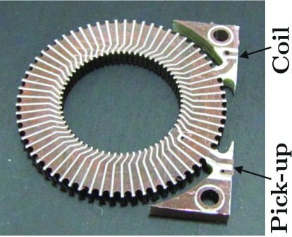
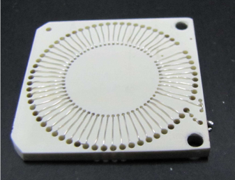
We produced this type of coil in-house and during multiple iterations, we varied the size and the number of vias. The lowest losses for our production process could be achieved with the design depicted in Fig. 3. The PCB coil has an outer diameter of 35mm and an inner diameter 20.4mm with a substrate thickness of 3.1mm. Its 64 windings result in an inductance of 1.4H. We added one winding which is galvanically isolated from the rest of the coil. This winding acts as an inductive pick-up and should thus be as reproducible as the entire coil.
3.2 Wire Coils
For the second type of coils, wire coils, we wound a single wire around
a rigid structure leading to a similar geometry as the PCB coils. Such
a coil is less reproducible than a PCB coil since the wire length will
vary for each coil. Hence, its inductance and its resistance will vary
as well. A coil with the same geometry
as for the PCB coils above, made out of
silver-plated copper on a Rogers 4350B substrate, is shown in
Fig. 4.
In wire coils, the cross-section of the core of a wire coil is bigger
than that of a PCB coil, because the wire bends are less sharp. Hence,
we expect the inductance of a wire coil to be higher than the one of a
PCB coil with the same nominal geometry. The 0.4mm thick
silver-plated copper wire, which we used for the wire coil, had a
cross-section similar to the average cross-section of a PCB
coil. Therefore, we expect similar losses in both types of coils with
the same geometries.
These considerations allow us to characterize the production processes
of the PCB coils by comparing the two types of coils.
Higher losses in the PCB coils are an indication that the production
of the PCB coils can be improved.
Since we do not need traces on the substrate, it is possible use any
machinable material with a low loss tangent. We also produced wire
coils with a Teflon core since it has a lower loss tangent and a lower
dielectric constant than Rogers 4350B. Thus, the losses will be less
affected by the core material and the self-resonance frequency of the
coil will be higher.
Another option to minimize the losses in the coil can be to use a
superconducting wire to reduce the ohmic losses of the resonator.
3.3 Spiral Coil
The quality factor of the presented coils are limited by the ohmic
resistance of the conductor. Thus, a coil based on a superconductor is
expected to result in lower losses in the resonator. Furthermore, it could
be necessary to operate the experiment at temperatures above 15K to
reduce the liquid helium consumption in wet cryostats. At these temperatures,
a superconductor with a
high critical temperature such as a high temperature superconductor (HTS)
is required. However, a coil made from a readily
available HTS material needs to be a two-dimensional (2D) structure due
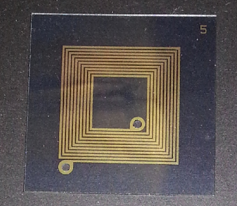
to manufacturing constraints, and we choose to use a spiral coil as shown
in Fig. 5.
Since such coils require only 2D structuring, they can be
manufactured in a very accurate and reproducible way. For the
demonstrated spiral coil, a high-temperature superconductor (HTS) was
produced by Ceraco Ceramic Coating222Ceraco Ceramic
Coating GmbH, Rote-Kreuz-Str. 8, D-85737 Ismaning, Germany. Our coils
were made out of an yttrium barium copper oxide (YBCO) film of 330nm
thickness on a sapphire wafer. To
facilitate soldered connections, a 200nm film of gold was placed on
top of the superconductor. The critical temperature of this YBCO film
is above 87K, and its critical current density is higher than A/cm2 at 77K. We can derive the peak current in the coil from
Section 2 to be 0.64A. Hence, traces
with a width of more than 100m are required to stay below the
critical current density.
For our square spiral coils, we chose a trace width of 300m, a
trace gap of 150m, and 10 windings. We designed 9 different
coils varying the outer diameter between 14 and 20mm. Equation 4.1 of
reference [19] gives an estimate for the inductance, which
results in target inductances between 1.2H and 1.6H for our coils.
This design should allow for coils with very high quality
factors already at temperatures accessible with liquid nitrogen
instead of liquid helium.
It should be noted here that superconductors are perfect diamagnets,
which are spatial inhomogeneities for magnetic fields. One can align
the 2D plane of the spiral coil with the spatially homogeneous magnetic
field of the experiment to minimize this effect, but one should
always keep this in mind.
4 Impedance Matching
The resonator is connected to the source through a cable with a given wave resistance , typically 50. The complex voltage reflection coefficient at the transition from the cable to the resonator [20] is then
| (9) |
where is the complex reflected voltage,
is the complex incoming voltage, and
is the complex impedance of the
resonator333The underline denotes a complex quantity.. The
reflected power coefficient is then just
. Since RLC-series resonators
have a very low impedance on resonance,
, the transition from a
50-cable to the resonator on resonance will reflect almost all
the inserted power. In order to minimize the reflection, a properly
designed impedance matching network is
required.
The most commonly used matching network is the -network as it is
the simplest, consisting only of two circuit elements.
Fig. 6 shows the two possible
-networks where the reactance parallel to the resonator transforms the
real part of the impedance to be . The resulting imaginary term
is small compared to (for low loss resonators) and can be
compensated with the series reactance.
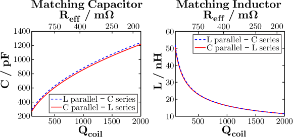
The resonator’s quality factor from (5) can be written as
| (10) |
for an RLC-series resonator. Fig. 7
shows the required values for the matching capacitor and inductance
as a function of the quality factor of the coil with inductance of
1.4H. For quality factors around 1000, the
required inductance is in the range of 10nH. Thin traces on a
PCB have approximately a length-dependent inductance of
1nH/mm. Therefore, small deviations in the trace length will lead to
inefficient matching. The strong dependence of the matching on the
reactance parallel to the resonator makes the matching network from
Fig. 6b) more favorable, because
capacitances of several hundred pF can be adjusted with much more
precision than inductances of about 10nH. One can incorporate the
inductance into the trace on the PCB from the coaxial connector
to the matching capacitance, by setting this distance between 1 and
2cm. Hence, we expect a power reflection of 1% or less even without
adding an additional inductor.
RF transformers or baluns on the RF input side are commonly used to
avoid ground loops between the RF source and the experiment. When
using the circuit from Fig. 6b) in
combination with a transformer, the DC potential of the trap
electrodes is not defined. We mitigate this by adding an RF-choke
parallel to the matching capacitor, where , as depicted in
Fig. 8.
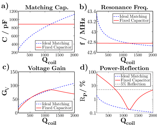
In a cryostat, it is impractical to adjust the matching capacitance
during or after a cool down. Hence, we have to find an
efficient way of choosing the best value for with a minimum
number of temperature cycles. For this, we simulated our matching
circuit for varying and also for a constant value of
. Fig. 9 shows results of
simulations where the fixed capacitor value was chosen for a match at
. Fig. 9a) depicts an
increase of the optimum with increasing
. Fig. 9b) illustrates the
dependence of the matched resonance frequency on . In
Fig. 9c), the simulations confirm the
dependence of the voltage gain on , following from (6). If the physical value for is smaller than
the expected value, used to chose the fixed matching capacitor, the
voltage gain is about the same than for an ideal match. But if the
actual quality factor is higher than the expected value,
the voltage gain will be lower than with an ideal match. Hence
underestimating the quality factor of the coil should be avoided since
it would result in a significantly lower voltage gain.
Fig. 9d) shows the reflection coefficient
as a function of . The effect of is small and thus it
was omitted for these simulations. We can see that even without
, but with an ideally matched , a low reflection coefficient
can be achieved. If one chooses a constant value for at a match
for , the reflected power will stay
below 5% even if varies between 800 and 2000.
The parameters for exact impedance matching can be estimated with one
additional cooling cycle. For the first cycle, one has to guess the
value for and adjust according to simulations
following the approach of Fig. 9a). When
the resonator is cold, the reflection coefficient is measured and
compared with the simulations in Fig. 9d). The measured reflection coefficient can then only
correspond to two values for . If the reflection
coefficient passed a minimum during cool-down, one should choose the
higher value, if not, the lower value of . With this new
value for , one can calculate the correct matching capacitor
value . Our experience shows that this method will yield a power
reflection coefficient of less than 2% for the second cool down.
5 RF Shield
RF resonators emit electromagnetic radiation, which needs to be
shielded to minimize unwanted RF interference in other parts of the
experiment. The RF shield needs to be grounded, and thereby generates a
capacitance between the resonator and ground. This capacitance has to
be minimized as suggested in (6). In order to keep
the resonator compact, we have to find a trade-off between the size of the
shield and the capacitance added by it.
First, we need to find a model for the shield capacitance
. Fig. 10 depicts a model where we
divide the coil in 2 half windings. Each has an ohmic resistance of
, an inductance , and a capacitance to the shield
. We can estimate with the standard formula for
a parallel-plate capacitor if we assume that the grounded shield is
parallel to the coil. From the calculations of the impedance of the
entire circuit, we can extract the effective capacitance that
occurs due to the presence of the shield.
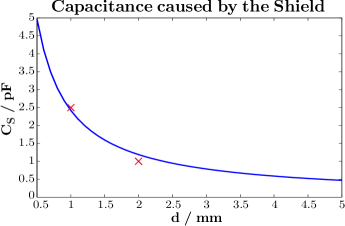
The results of these simulations for our PCB coils with an outer
radius of 17.5mm and an inner radius of 10.2mm are shown in
Fig. 11. It can be seen that a distance of
about 2mm is sufficient to keep the additional capacitive load below
1pF. Adapted simulations for the wire coils yield results similar to
the ones for the PCB coils. Hence, we can use the same shield for both
types of coils.
We expect that the capacitance caused by the shield for the spiral
coils is even smaller, because its surface is smaller. Additionally, if
we place the spiral coil in the center of the same shield, the distance
to the shield will be 1.55mm bigger than for the other coils.
Hence, the capacitance to ground will decrease further.
Moreover, the shield has an influence on the magnetic field lines of
the spiral coil in this configuration and thereby also on the inductance
and the losses of the coil.
At room temperature, the penetration depth due to skin effect in
copper at frequencies around 40MHz is about 10m. Thus, any
mechanically stable shield, of a couple of 1/10mm thickness,
should yield a suitable attenuation.
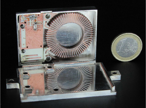
Fig. 12 shows a resonator encased in a
silver-plated copper shield. The dimensions of this resonator are 57mm
x 40mm x 10.2mm. On the left side of the resonator, one can see a PCB
with the matching network at the top and the SMT-connector for the
inductive pick-up at the bottom. On the right side is the PCB coil,
and the two PCBs are connected together by soldered joints.
6 Results
In our measurement setup, we used a capacitive pick-up to measure the
voltage at the trap. With the known ratio of this capacitive voltage
divider, we could directly measure the voltage at the trap and
calibrate the inductive pick-up of the coil.
| Name | T | |||
| PCB coil | 295K | 42.4MHz | 19.4 | 60 |
| PCB coil | 80K | 42.8MHz | 27.1 | 115 |
| PCB coil | 10K | 42.9MHz | 41.5 | 208 |
| Wire Coil | 295K | 36.8MHz | 25.2 | 89 |
| Wire Coil | 80K | 37.2MHz | 36.5 | 184 |
| Wire Coil | 10K | 37.9MHz | 58.9 | 624 |
| HTS Coil | 88K | 44.3MHz | 92.1 | 1172 |
Table 1 shows our measurement
results. The PCB coils had an inductance very close to the desired
value. Unfortunately, we could not achieve the expected quality
factor. We had designed the wire coils to have losses
similar to the PCB coils, but the PCB coils showed much higher losses
than the wire coils. We think this is due to an imperfect production
process that we could not improve further with our in-house techniques.
Additionally to the PCB coils in copper, we produced them in silver as
well. The inductances were similar, but the losses in the silver coils
were even higher. This was unexpected as silver is a better conductor
than copper. But the silver coils needed to be reworked after fabrication
to remove shorts between the segments. During this process, the silver coating
might have been scratched, resulting in higher losses. We expect that
silver plating after structuring should reduce the losses compared to
a copper coil, but we were unable to do so with our in-house
fabrication process.
The voltage gain of about 60 of the wire coil would require 160mW RF
input power to get to the desired 170 at the trap. If we
adjust the voltage to keep the stability parameter , only
100mW RF input power are required at the modified resonance frequency.
We expect that one can improve the quality factor of the wire coil by
using a thicker wire. We also tested a resonator with a lead-plated
wire, which did not show an increased voltage gain. We either could
not reach the critical temperature of lead in our test setup, or the
lead was not pure enough to become superconducting.
The spiral coil showed the highest voltage gain, although the shield
influences the magnetic field generated by the coil. We observed a
change of the resonance frequency of a couple of percent when cooling
down from liquid nitrogen temperatures to liquid helium temperatures,
which we attribute to the shield surrounding the coil. With a
voltage gain of 92, one would need about 70mW of RF input power to get
170. With a stability parameter at the higher
resonance frequency, it would be 82mW.
7 Conclusion
We have demonstrated three designs of RF resonators for trapped ion
experiments with Paul traps. The PCB coils have favorable mechanical
properties but still need an improved production process, such as
e.g. thermal annealing. The wire coils fulfill our criteria and can
be further improved by using a thicker or superconducting wire. The
HTS spiral coil showed the highest voltage gain, which was already
accessible at temperatures reached with liquid nitrogen cooling.
Efficient matching is usually difficult in a cryogenic environment
because normally one cannot tune the matching parameters when the
cryostat is cold. We have shown a recipe to efficiently match
RLC-resonators without precise knowledge of their quality factors.
During this empirical study we regularly achieved matching with a
power reflection of less than 2% on the second cool-down. Additionally, we
designed and implemented a shield for resonators to minimize RF
pick-up in other parts of the experiment.
8 Acknowledgments
We thank Gerhard Hendl from the Institute of Quantum Optics and Quantum Information of the Austrian Academy of Science for the production of PCBs, and PCB coils for this study. Furthermore, we want to thank Florian Ong for feedback on the manuscript. This research was funded by the Office of the Director of National Intelligence (ODNI), Intelligence Advanced Research Projects Activity (IARPA), through the Army Research Office grant W911NF-10-1-0284. All statements of fact, opinion or conclusions contained herein are those of the authors and should not be construed as representing the official views or policies of IARPA, the ODNI, or the U.S. Government.
References
- [1] W. Paul, Rev. Mod. Phys. 62 (1990) 531-540
- [2] M. Chwalla, J. Benhelm, K. Kim, G. Kirchmair, T. Monz, M. Riebe, P. Schindler, A.S. Villar, W. Haensel, C. F. Roos, R. Blatt, M. Abgrall, G. Santarelli, G. D. Rovera, Ph. Laurent, Phys. Rev. Lett. 102 (2009) 023002
- [3] H. S. Margolis, G. Huang, G. P. Barwood, S. N. Lea, H. A. Klein, W. R. C. Rowley, P. Gill, R. S. Windeler, Phys. Rev. A 67 (2003) 032501
- [4] J.I. Cirac, P. Zoller, Phys. Rev. Lett. 74 (1995) 4091-4094
- [5] D. Kielpinski, C. Monroe, D.J. Wineland, Nature 417 (2002) 709-711
- [6] T. Monz, P. Schindler, J.T. Barreiro, M. Chwalla, D. Nigg, W.A. Coish, M. Harlander, W. Hänsel, M. Hennrich, R. Blatt Phys. Rev. Lett. 106 (2011) 130506
- [7] D. Porras, J.I. Cirac, Phys. Rev. Lett. 92 (2004) 207901
- [8] P. Jurcevic, B.P. Lanyon, P. Hauke, C. Hempel, P. Zoller, R. Blatt, C.F. Roos, Nature 511 (2014) 202-205
- [9] Q.A. Turchette, B.E. King, D. Leibfried, D.M. Meekhof, C.J. Myatt, M.A. Rowe, C.A. Sackett, C.S. Wood, W. Itano, C. Monroe, D. J. Wineland, Physical Review A 61 (2000) 063418
- [10] J. Labaziewicz, Y. Ge, P. Antohi, D. Leibrandt, K. R. Brown, I. L. Chuang, Physical Review Letters 100 (2008) 013001
- [11] W.W. Macalpine, R.O. Schildknecht, Proc. IRE 47 (1959) 2099-2105
- [12] J.D. Siverns, L.R. Simkins, S.Weidt, W.K. Hensinger, Appl. Phys. B 107 (2012) 921-934
- [13] S.R. Jefferts, C. Monroe, E.W. Bell, D.J. Wineland, Phys. Rev. A 51 (1995) 3112-3116
- [14] M. E. Poitzsch, J. C. Bergquist, W. M. Itano, D. J. Wineland, Rev. Sci. Instrum. 67 (1996) 129-134
- [15] D. Gandolfi, M. Niedermayr, M. Kumph, M. Brownnutt, R. Blatt, Rev. Sci. Instrum. 83 (2012) 084705
- [16] D. J. Wineland, C. Monroe, W. M. Itano, D. Leibfried, B. E. King, D. M. Meekhof, Journal of Research of the National Institute of Standards and Technology 103 (1998) 259-328
- [17] J. W. Ekin, Experimental Techniques For Low-Temperature Measurements (Oxford University Press, 2006) 504-505
- [18] P. Kamby, A. Knott, M.A.E. Andersen, IECON 2012 - 38th Annual Conference on IEEE Industrial Electronics Society (2012) 680-684
- [19] S. S. Mohan, The design, modeling and optimization of on-chip inductor and transformer circuits (Ph.D. thesis, Department of Electrical Engineering, Stanford University, 1999)
- [20] D.M. Pozar, Microwave Engineering (John Wiley & Sons, 2011)