Lower limits of line resistance in nanocrystalline Back End of Line Cu interconnects
Abstract
The strong non-linear increase in Cu interconnect line resistance with decreasing linewidth presents a significant obstacle to their continued downscaling. In this letter we use first principles density functional theory based electronic structure of Cu interconnects to find the lower limits of their line resistance for metal linewidths corresponding to future technology nodes. We find that even in the absence of scattering due to grain boundaries, edge roughness or interfaces, quantum confinement causes a severe increase in the line resistance of Cu. We also find that when the simplest scattering mechanism in the grain boundary scattering dominated limit is added to otherwise coherent electronic transmission in monocrystalline nanowires, the lower limit of line resistance is significantly higher than projected roadmap requirements in the International Technology Roadmap for Semiconductors.
Damascene deposited Copper has been the Back End of Line (BEOL) interconnect conductor of choice for semiconductor technology nodes since 2000. Copper has several desirable features, including a low bulk resistivity ( 1.68 cm at room temperature, second only to Ag among elemental metals Giancoli (2008)) and the ability to easily be electro-deposited and annealed at temperatures compatible with semiconductor processing.
With metal linewidth scaling proceeding in sync with technology scaling, it should be expected that the resistance per unit length (henceforth referred to as with units in m) of BEOL Cu metallization will increase. It has been known for some time, however, that metal resistivity also increases with a decrease in metal dimensionality Sondheimer (1952). This adds to the increase in that is expected from a simple reduction in dimensions. This increase in metal resistivity has been attributed to an increase in electron scattering due to grain boundaries Mayadas and Shatzkes (1970), surfaces and interfaces Fuchs (1938); Sun et al. (2009, 2010). Consequently, the International Technology Roadmap for Semiconductors (ITRS) has projected an increase in roadmap effective metal resistivity (for the lowest BEOL metallization level or M1) from 4.77 -cm in 2016 to 11.41 -cm by the year 2028 wil (2013). This corresponds to a significant increase in projected requirement from approximately 35 m in the year 2016 to 1180 m in the year 2028.
To determine if Cu can meet this requirement, we use first principles Density Functional Theory (DFT) based electronic structure simulations of Cu to find the lower limits of its line resistance for metal linewidths corresponding to future technology nodes. These lower limits are then compared to ITRS projected requirements for the lowest Back End of Line metallization level (M1)wil (2013).
The motivation for a lower limits investigation is that if the lower limits are sufficiently below projected requirements, then they can be achieved through continued improvements in BEOL resistance engineering. If the lower limits themselves are significantly above projected requirements, it serves to re-evaluate if Cu is suitable for future nodes. Our investigation is similar in spirit to previous calculations on the lower limits of contact resistivity in Si Maassen et al. (2013); Hegde and Bowen (2014).
We wish to state explicitly what we mean by ’lower limits of line resistance’ in this letter. In the absence of any electron scattering mechanism such as that due to phonons, impurities, interfaces and grain boundaries, conductance is decided simply by the number of conducting channels available. If we translate this definition for the case of Cu interconnects, we infer that the ballistic/Landauer limit of conductance of monocrystalline nanowires in the coherent transport regime represents the upper limit of Cu interconnect conductance and their corresponding resistance represents the lower limit Datta (2005). While the resistance of monocrystalline nanowires represents the theoretical lower limit, they do not (yet) represent a practically achievable lower limit. The processes involved in the formation of Cu interconnects result in, at best, structures with a high concentration of low specific resistivity [111]/[111] twin boundaries of Coincidence Site Lattice (CSL) type Lu et al. (2004). A practically achievable lower limit would therefore consist of nanowires with such twin boundaries along the direction of transport.
In this letter we therefore report both theoretical and practical lower limits. The rest of this letter is organized as follows. We first present the details of our computational method, followed by line resistance calculations versus cross sectional area for monocrystalline nanowires oriented along 6 different transport directions. Next, the simplest grain boundary scattering mechanism - twin [111]/[111] 3 boundaries are added to [111] oriented nanowires and their versus cross sectional area is compared to ITRS requirements. Finally, we compare the line resistance between these ideal twin structures and their more realistic nanocrystalline counterparts. We then conclude with a discussion on the implications of our lower-limits study.
We note here that DFT has been shown in past literature to accurately reproduce the bulk Fermi Surface and resistivity of metal nanostructuresFeldman et al. (2010); Hegde et al. (2014a, b); Kim et al. (2010); Ke et al. (2009); Timoshevskii et al. (2008); Zhou et al. (2010). The usual procedure followed in several of the aforementioned studies is the computation of the self-consistent electronic density of the metal structures, followed by a Landauer-Buttiker analysis of electrical conductance Datta (2005). This is the procedure we follow in this work as well. We first compute ballistic conductance of monocrystalline Cu nanowire structures oriented along six transport orientations - [100], [110], [111], [112], [120] and [122] - using the Landauer-Buttiker formalism. The cross sectional areas of the monocrystalline structures studied ranged from 20 to 100 nm2. The choice of orientations was motivated by the dominant orientations of grains seen in the direction of transport in damascene deposited Cu interconnects Ganesh et al. (2012). The ballistic conductance in this formalism is given as G = where
| (1) |
where is energy, is the quantum of conductance, is the net number of modes at energy and is the Fermi function). The net number of modes is obtained by computing the self-consistent band structure and simply counting the number of conducting modes at each energy step broadened by the Fermi function. Cu nanowires with cross sectional areas of 100 nm2 contain between 5000 to 15000 atoms (depending on the orientation). Computing the self consistent band structure of such a large number of atoms in DFT is computationally cumbersome. To enable scaling of DFT calculations to the required system size, a recently published s-orbital approximation to the basis of Cu was used to compute the self consistent band structure of the nanowires Hegde and Bowen (2015). For additional details of the computational procedure, we refer the interested reader to this work.
Ballistic conductance is independent of the length of the cross section in the transport direction. To compute line resistance per unit length a length scale corresponding to a scattering event is introduced. Here we assume a scattering length equal to bulk inelastic mean free path in Cu (400Å). It has been shown Datta (2005) that an introduction of a scattering mean free path in the Landauer-Buttiker formalism modifies the ballistic conductance G as follows
| (2) |
where is the scattering mean free path, which we approximate to be independent of energy. Since M1 interconnect run lengths () range in microns, we have , this results in
| (3) |
Using the bulk mean free path is a rather generous assumption, given that the width of the nanowires investigated is a maximum of 10 nm. It is thus safe to say that the numbers for monocrystalline Cu nanowires represent the lower limit of line resistance in Cu interconnects.
To compare our simulations to ITRS projections, we used projected Cu requirements for resistivity data available in the 2013 ITRS table (see MPU Interconnect Technology requirements for M1 level in the roadmap wil (2013)) and calculate projected requirements for cross sectional areas between 20 to 100 nm2. Damascene Cu lines are bounded by a cladding/barrier layer on two sidewalls and the trench bottom. We subtracted the barrier/cladding thickness outlined in the ITRS table from the trench bottom and from each sidewall to obtain the effective Cu cross sectional area . The ITRS projection was then computed by dividing the conductor effective resistivity (obtained from aforementioned table) by in line with Ohm’s law.
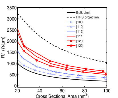
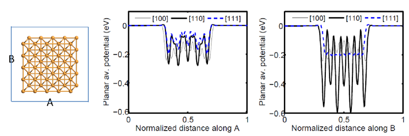
Figure 1 shows a comparison of lower limits for different Cu orientations obtained from DFT and ITRS projected requirements for Cu cross sectional areas (i.e. without liner and barrier) between 20 and 100 nm2. For the sake of reference, the bulk lower limit (obtained by averaging the bulk ballistic transmission over the Fermi surface of Cu) is also plotted. It is evident that the lowest limit in Cu is determined by [110] oriented monocrystalline nanowires. It can also be seen that this lowest limit in monocrystalline Cu [110] is well below ITRS projected requirements for all cross sectional areas shown.
The mismatch in line resistance between nanowire orientations comes from the anisotropy in the ballistic conductance between orientations that has been discussed in previous publications Hegde et al. (2014b); Jones et al. (2015). The conductance anisotropy under confinement for a prototypical metal such as Cu that has an approximately spherical bulk Fermi surface can in turn be explained by reference to the planar averaged electrostatic potential in the nanowires along the direction of confinement. Figure 2 shows such a comparison for three nanowire orientations of equal cross sectional area. It is evident that the confining potential varies quite strongly for the nanowires oriented differently. This anisotropy in quantum confinement potential leads to an anisotropy in conducting modes.
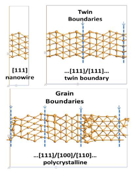
As mentioned previously, while the calculation of for monocrystalline nanowires may indicate a theoretical limit that is lower than ITRS projected requirements, we are unaware of a practical method to pattern perfectly monocrystalline metal interconnects on a large scale required for semiconductor technology. Existing techniques such as electrodeposition used in the damascene process result in interconnects that are polycrystalline with a wide variation in the grain orientation distribution Ganesh et al. (2012). It has, however, been demonstrated that Cu nanowires with a high degree of ’twinning’ along the [111] transport direction can be fabricated Lu et al. (2004). Recent DFT calculations of the specific resistivity of grain boundaries also indicate that the [111]/[111] 3 Coincidence Site Lattice (CSL) or twin boundary has the least specific resistivity among all grain boundaries César et al. (2014). This has been attributed to negligible bond-orientational disorder seen at such boundaries compared to other grain boundaries. It is therefore reasonable to infer that the values of nanowires with [111]/[111] 3 twin boundaries along transport direction represent a more practically achievable lower limit.
The calculations performed on monocrystalline nanowires were therefore repeated for nanowires consisting of [111]/[111] twin boundaries along the direction of transport. Since a significant impact of Aspect Ratio (AR) was not seen for monocrystalline nanowires, we limited the calculations to an AR of 11. Figure 3 shows an example of such a twin boundary structure. In keeping with data from recent experiments and other simulation studies of the Cu interconnect system Roberts, Kaushik, and Clarke (2015); Pyzyna et al. (2015), grain size was assumed to equal line width. As shown in figure 3, the eventual structure simulated consists of twin grains infinitely repeated along the direction of transport. values for cross sectional areas up to 60 nm2 (system size of up to 25000 atoms) were fit and projected up to cross sectional areas of 100 nm2.
The results of the calculation for twin boundary structures and its comparison to ITRS projections is shown in figure 4. It is very clear that a change from [111] oriented monocrystalline to the simplest boundary - that of [111]/[111] twin structures - results in an increase in values to the extent that these are now higher than projected ITRS requirements. This is even after discounting the fact that we used the bulk scattering mean free path for the twin boundary structures even though the grain size was significantly smaller than the mean free path used.
It must be emphasized that the twin boundary structures considered in this study are highly ordered. Process related non-idealities such as grain orientation anisotropy (GOA), line edge roughness, and the presence of a Cu-liner interface will result in actual values that are higher than this ideal case. GOA, especially, will result in a significant resistance penalty owing to increased anisotropy in conductance for different orientations when Cu is quantum confined as discussed previously. To estimate the impact of more realistic structures on line resistance, we simulated a large number of polycrystalline structures with a wide variety of grain orientation distributions for each cross sectional area. We retained the structural assumptions regarding aspect ratio and grain size made for twin boundaries. An example of such a structure is shown in figure 3. We then averaged the ballistic conductance for all of these structures and computed an averaged value representative of all structures simulated. The resultant line resistance shown in figure 4 is significantly higher than the limits of twin boundary structures and ITRS projections.
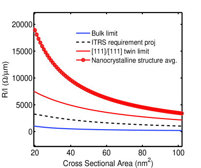
The results presented in this letter indicate that from a materials perspective, nanocrystalline Cu will not be able to meet projected ITRS requirements. While remedial measures such as reduction in GOA, increase in grain size and a reduction in barrier thickness may improve Cu line resistance significantly, it is not possible to completely eliminate either grain boundaries or barriers and liners in the current damascene Cu BEOL paradigm. Additionally, if BEOL scaling is to be maintained, then confinement and its concomitant effects such as the severe rise in line resistance shown previously are unavoidable. Even the best case that can practically be engineered - that of 3 twin boundaries - does not seem to meet projected requirements. While a exhaustive exploration of all possible grain orientation distributions is not feasible even in simulation, the values of the polycrystalline structures we calculated serve to illustrate the extent to which the aforementioned structural imperfections increase line resistance well beyond ITRS requirements.
In conclusion, we reported the results of our investigation into the lower limits of line resistance in Cu interconnects. We found that simple confinement results in a significant increase in Cu line resistance. When the simplest grain boundary scattering mechanism - scattering at highly ordered [111]/[111] 3 twin boundaries - was introduced into otherwise ballistic monocrystalline [111] interconnects, we found that the limits increase beyond ITRS projected requirements. This increase in line resistance presents a significant obstacle to the continued use of Cu interconnects in future technology nodes. We believe that the results of this investigation warrant increased attention on schemes and materials that mitigate the potentially rapid rise in BEOL resistance in future technology nodes.
We thank Titash Rakshit, Borna Obradovic and Rwik Sengupta for helpful suggestions made during the course of this work.
References
- Giancoli (2008) D. C. Giancoli, Physics for scientists and engineers with modern physics (Pearson Education, 2008).
- Sondheimer (1952) E. H. Sondheimer, “The mean free path of electrons in metals,” Advances in physics 1, 1–42 (1952).
- Mayadas and Shatzkes (1970) A. Mayadas and M. Shatzkes, “Electrical-resistivity model for polycrystalline films: the case of arbitrary reflection at external surfaces,” Physical Review B 1, 1382 (1970).
- Fuchs (1938) K. Fuchs, “The conductivity of thin metallic films according to the electron theory of metals,” in Mathematical Proceedings of the Cambridge Philosophical Society, Vol. 34 (Cambridge Univ Press, 1938) pp. 100–108.
- Sun et al. (2009) T. Sun, B. Yao, A. P. Warren, K. Barmak, M. F. Toney, R. E. Peale, and K. R. Coffey, “Dominant role of grain boundary scattering in the resistivity of nanometric cu films,” Physical Review B 79, 041402 (2009).
- Sun et al. (2010) T. Sun, B. Yao, A. P. Warren, K. Barmak, M. F. Toney, R. E. Peale, and K. R. Coffey, “Surface and grain-boundary scattering in nanometric cu films,” Physical Review B 81, 155454 (2010).
- wil (2013) “International technology roadmap for semiconductors (itrs), interconnects section,” Semiconductor Industry Association (2013).
- Maassen et al. (2013) J. Maassen, C. Jeong, A. Baraskar, M. Rodwell, and M. S. Lundstrom, “Full band calculations of the intrinsic lower limit of contact resistivity,” Applied Physics Letters (2013).
- Hegde and Bowen (2014) G. Hegde and R. C. Bowen, “Effect of realistic metal electronic structure on the lower limit of contact resistivity of epitaxial metal-semiconductor contacts,” Applied Physics Letters 105, 053511 (2014).
- Feldman et al. (2010) B. Feldman, S. Park, M. Haverty, S. Shankar, and S. T. Dunham, “Simulation of grain boundary effects on electronic transport in metals, and detailed causes of scattering,” physica status solidi (b) 247, 1791–1796 (2010).
- Hegde et al. (2014a) G. Hegde, M. Povolotskyi, T. Kubis, T. Boykin, and G. Klimeck, “An environment-dependent semi-empirical tight binding model suitable for electron transport in bulk metals, metal alloys, metallic interfaces, and metallic nanostructures. I. model and validation,” Journal of Applied Physics 115, 123703 (2014a).
- Hegde et al. (2014b) G. Hegde, M. Povolotskyi, T. Kubis, J. Charles, and G. Klimeck, “An environment-dependent semi-empirical tight binding model suitable for electron transport in bulk metals, metal alloys, metallic interfaces, and metallic nanostructures. II. Application - Effect of quantum confinement and homogeneous strain on cu conductance,” Journal of Applied Physics 115, 123704 (2014b).
- Kim et al. (2010) T.-H. Kim, X.-G. Zhang, D. M. Nicholson, B. M. Evans, N. S. Kulkarni, B. Radhakrishnan, E. A. Kenik, and A.-P. Li, “Large discrete resistance jump at grain boundary in copper nanowire,” Nano letters 10, 3096–3100 (2010).
- Ke et al. (2009) Y. Ke, F. Zahid, V. Timoshevskii, K. Xia, D. Gall, and H. Guo, “Resistivity of thin cu films with surface roughness,” Physical Review B 79, 155406 (2009).
- Timoshevskii et al. (2008) V. Timoshevskii, Y. Ke, H. Guo, and D. Gall, “The influence of surface roughness on electrical conductance of thin cu films: an ab initio study,” Journal of Applied Physics 103, 113705 (2008).
- Zhou et al. (2010) B.-h. Zhou, Y. Xu, S. Wang, G. Zhou, and K. Xia, “An ab initio investigation on boundary resistance for metallic grains,” Solid State Communications 150, 1422–1424 (2010).
- Datta (2005) S. Datta, Quantum transport: atom to transistor (Cambridge University Press, 2005).
- Lu et al. (2004) L. Lu, Y. Shen, X. Chen, L. Qian, and K. Lu, “Ultrahigh strength and high electrical conductivity in copper,” Science 304, 422–426 (2004).
- Ganesh et al. (2012) K. Ganesh, A. Darbal, S. Rajasekhara, G. Rohrer, K. Barmak, and P. Ferreira, “Effect of downscaling nano-copper interconnects on the microstructure revealed by high resolution tem-orientation-mapping,” Nanotechnology 23, 135702 (2012).
- Hegde and Bowen (2015) G. Hegde and R. C. Bowen, “On the feasibility of ab initio electronic structure calculations for cu using a single s orbital basis,” AIP Advances 5, 107142 (2015).
- Fonseca et al. (2013) J. E. Fonseca, T. Kubis, M. Povolotskyi, B. Novakovic, A. Ajoy, G. Hegde, H. Ilatikhameneh, Z. Jiang, P. Sengupta, Y. Tan, et al., “Efficient and realistic device modeling from atomic detail to the nanoscale,” Journal of Computational Electronics 12, 592–600 (2013).
- Jones et al. (2015) S. L. Jones, A. Sanchez-Soares, J. J. Plombon, A. P. Kaushik, R. E. Nagle, J. S. Clarke, and J. C. Greer, “Electron transport properties of sub-3-nm diameter copper nanowires,” Physical Review B 92, 115413 (2015).
- César et al. (2014) M. César, D. Liu, D. Gall, and H. Guo, “Calculated resistances of single grain boundaries in copper,” Physical Review Applied 2, 044007 (2014).
- Roberts, Kaushik, and Clarke (2015) J. M. Roberts, A. P. Kaushik, and J. S. Clarke, “Resistivity of sub-30 nm copper lines,” in Interconnect Technology Conference and 2015 IEEE Materials for Advanced Metallization Conference (IITC/MAM), 2015 IEEE International (IEEE, 2015) pp. 341–344.
- Pyzyna et al. (2015) A. Pyzyna, R. Bruce, M. Lofaro, H. Tsai, C. Witt, L. Gignac, M. Brink, M. Guillorn, G. Fritz, H. Miyazoe, et al., “Resistivity of copper interconnects beyond the 7 nm node,” in VLSI Technology (VLSI Technology), 2015 Symposium on (IEEE, 2015) pp. T120–T121.