Weak Antilocalization and Universal Conductance Fluctuations in Bismuth Telluro-Sulfide Topological Insulators
Abstract
We report on van der Waals epitaxial growth, materials characterization and magnetotransport experiments in crystalline nanosheets of Bismuth Telluro-Sulfide (BTS). Highly layered, good-quality crystalline nanosheets of BTS are obtained on SiO2 and muscovite mica. Weak-antilocalization (WAL), electron-electron interaction-driven insulating ground state and universal conductance fluctuations are observed in magnetotransport experiments on BTS devices. Temperature, thickness and magnetic field dependence of the transport data indicate the presence of two-dimensional surface states along with bulk conduction, in agreement with theoretical models. An extended-WAL model is proposed and utilized in conjunction with a two-channel conduction model to analyze the data, revealing a surface component and evidence of multiple conducting channels. A facile growth method and detailed magnetotransport results indicating BTS as an alternative topological insulator material system are presented.
pacs:
73.20.At,72.20.My,73.25.+i,81.15.KkI Introduction
Bismuth (Bi) and Antimony (Sb) based binary chalcogenide compounds have received widespread attention in the last few years for exhibiting rich physics of strong 3D topological insulators (TI), matching theoretical predictions of time-reversal invariant and gapless surface states with spin-momentum locked Dirac fermions Fu and Kane (2007); Hasan and Kane (2010); Ando (2013). Applications of TI heterostructure devices range from topological quantum computing with Majorana fermionsHasan and Kane (2010), spin-based logic and memoryPesin and MacDonald (2012) and axion electrodynamicsLi et al. (2010). Electronic and spintronic device applications of TI often involve manipulating the electronic surface states, and hence uncovering the details of the underlying transport mechanism is an important aspect of current research. The binary phases (Bi, Sb)2(Se, Te)3 have been explored extensively as 3D TI materials from the standpoint of transport experimentsChen et al. (2010); Steinberg et al. (2010); He et al. (2011); Wang et al. (2011); Liu et al. (2011); Chen et al. (2011); Steinberg et al. (2011); Bansal et al. (2012); Taskin et al. (2012); Takagaki et al. (2012a); Roy et al. (2013); Ando (2013). Transport experiments often involve the non-negligible contribution from the bulk, which complicates the electronic probing of surface states. Attributing the indirect signatures to multiple conduction channels has been the focus of intense researchAndo (2013); Chen et al. (2011); Steinberg et al. (2011); Taskin et al. (2012); Bansal et al. (2012); Lee et al. (2012); Kim et al. (2013); Yang et al. (2014), prompting the need to further explore transport in multiple TI material systems. An attractive direction to explore is ternary (or quaternary) compounds M2X3-xYx (M = {Bi, Sb, Bi1-ySby}, X, Y = {Te, Se, S}), as the material properties, and consequently transport properties, can be tuned by the addition of other elementsRen et al. (2010); Wang and Johnson (2011); Kong et al. (2011); Lee et al. (2012); Xia et al. (2013); Ando (2013). The Sulfur-based ternary compound (naturally occurring tetradymite with an ideal formula Bi2Te2S) has received relatively little attention from a transport perspective, even as it is theoretically predicted to be a promising 3D TIWang and Johnson (2011). The Sulfur based tetradymite has been synthesized in the laboratory as bulk crystals in previous experiments, albeit showing non-stoichiometry in deviation from the ideal structureSoonpaa (1962); Glatz (1967); Pauling (1975); Ji et al. (2012). The substitution of a more electronegative S for Te in the Bi2Te3 crystal structure is expected to increase the bulk band gap, reduce antisite defects and exposes the otherwise buried Dirac pointWang and Johnson (2011); Ji et al. (2012), as has been observed in promising angle-resolved photoemission spectroscopy (ARPES) experiment on bulk crystals of the materialJi et al. (2012). The tetradymite ternary thus provides a promising platform to study transport signatures of the surface states.
We report on the van der Waals epitaxial growth of crystalline Bismuth Telluro-Sulfide (BTS) nanosheets and observation of surface states through transport experiments. Low-temperature insulating ground state in the conductivity of the BTS devices reveals the presence of electron-electron interaction (EEI) effects, which have been observed for thin films of 3D TIs. The characteristic weak antilocalization (WAL) signature of the topological surface states is seen in the magnetoresistance, which acts in combination with EEI effects at low-temperatures and low-fields. Evidence of separation of transport channels in Hall data is seen, with a parallel conductivity contribution from bulk states. A two-channel Hall conductance model is used in conjunction with an extended WAL fit to describe the results. Universal conductance fluctuations (UCF) are also observed in the magnetoresistance of thin BTS devices, the temperature-dependent behavior of which is analyzed with standard UCF theory for two-dimensional metals, yielding phase coherence lengths of the same order as those obtained from WAL. Empirical parameters from modeling the thickness- and temperature-dependent WAL and UCF data indicate two-dimensional mesoscopic transport, revealing the presence of accessible surface states in the BTS material system.
II Experimental Methods
II.1 van der Waals epitaxial Growth
The BTS nanosheets are grown by hot-wall van der Waals epitaxy (vdWE) with a combination of compound solid-state precursors, in a 60mm diameter quartz tube inside a three-zone furnace. Low-resistivity ( 5 cm) silicon wafers are thermally oxidized to grow high quality nm thick SiO2. An alignment marker grid for e-beam lithography is then etched into the SiO2 film with standard photolithography and dry etch, instead of depositing metallic markers. Metal alignment markers are found to act as nucleation centers leading to undesirably thick, dense and malformed growth with possible metal contamination, hence etched-in alignment markers are preferred. SiO2/Si wafers so prepared are then cleaved into samples of 5-20 mm size and placed either vertically or horizontally in a slotted quartz carrier. The quartz carrier is placed at the neck of the furnace in the cold-zone, downstream of the precursor materials (16” away from central zone). Muscovite mica samples of similar sizes are freshly cleaved immediately prior to growth and loaded inside in a similar fashion. Powdered Bi2Te3 (4N Sigma-Aldrich) is placed in a quartz boat in the center zone, along with chunks of Bi2S3 (5N Sigma-Aldrich), either in the same boat or in another boat in the zone closer to the sample carrier. The quartz tube is then pumped down to base pressure several times and subsequently purged with N2 gas for a few hours to remove any trace oxygen and moisture, and to achieve a stable pressure and flow of the carrier gas. All three zones of the furnace are then heated up to C within 20 minutes without overshooting and are held at that temperature for minutes before being cooled down naturally to room temperature. Good growth is observed when tube pressure is in the range of Torr with N2 flow in the range of sccm and when the samples are in the temperature range of C. Representative samples are analyzed with Raman spectroscopy and X-ray diffraction to confirm crystalline nature of the growth. Compositional analysis is performed on candidate nanosheets with Carl Zeiss/EDAX energy dispersive x-ray spectroscope to confirm the presence of all three elements within a range of stoichiometries. Tellurium-rich nanostructures are obtained for sample temperatures lower than C, as has been observed before in a similar growth experimentTakagaki et al. (2011).
II.2 Device Fabrication
As-grown samples of BTS on SiO2 are inspected using an optical microscope and AFM to identify flat and thin ( nm) candidate nanosheets, with lateral dimensions in the range of a few microns. Contacts are patterned directly on the as-grown nanosheets in a four-point or Hallbar geometry with standard e-beam lithography and liftoff. Immediately prior to metallization, the contact areas on the BTS nanosheet are etched with a brief Ar plasma (10-12 s, 75 W) in an RIE chamber using the e-beam resist as the etch mask, to remove surface oxides and other contaminants. A or nm of Ti/Pd or Ti/Au metal stack is deposited with e-beam evaporation for the contact leads. The samples are then attached onto a standard 16-pin DIP package with silver-paste and wirebonded using a Au ball-bonder or an Al wedge-bonder. Sample temperature during the fabrication process is carefully maintained below C to prevent material degradation.
II.3 Transport Measurements
The wirebonded samples are loaded inside Quantum Design EverCool2 PPMS system, equipped with a T magnet. All magnetotransport measurements are performed using Stanford Research Systems 830 digital lock-in amplifiers. A steady current in the range of is supplied to the two outer terminals of the Hallbar. The current source is formed by the sinusoidal voltage output of the SRS-830 and a standard series resistor. The series resistor is in the range of 1 M, whereas the typical DUT resistances are of the order of 1 k or less. Hence, the current fluctuation due to the DUT series-loading is three orders of magnitude lower and can be safely ignored. Four-point longitudinal () and transverse () resistances are measured as a function of the magnetic field , with two phase-locked lock-in amplifiers at low frequency ( Hz). The symmetric functions are calculated as: and . Temperature dependent measurements are performed down to a chamber temperature of 2 K, and magnetic field sweeps are up to T.
III Results and Discussion
III.1 Growth, Structural and Chemical Characterization
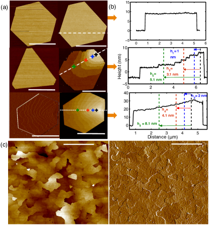
The ability to grow any layered material on top of any other layered or a 3D bulk materialKoma (1999) makes vdWE a versatile and convenient method to synthesize novel materials. Bi and Sb chalcogenide compounds have been grown using vdWE on 3D substratesFerhat et al. (1996); Kong et al. (2011); Takagaki et al. (2011); Hao et al. (2012), layered substrates such as micaPeng et al. (2012), hexagonal Boron NitrideGehring et al. (2012) and grapheneDang et al. (2010). The hot-wall vdWE technique is preferable for growing thin-films of TI compounds containing Sulfur, as the high vapor-pressure of Sulfur makes it an undesirable source material for most molecular beam epitaxy (MBE) systems. The vdWE-grown BTS nanosheets show clear crystal shape-symmetry, growing largely in hexagonal and truncated-triangular shapes of lateral dimensions of a few microns, as seen in Fig-1(a). The underlying crystal symmetry of BTS is trigonal-hexagonal (space group ), which leads to the formation of layered triangular nanosheets during growth. Similar terraced growth has also been observed for other 2D material systems with trigonal symmetry, on different substratesMichely et al. (1993); Roy et al. (2013, 2015). After the initial nucleation of the islands, the ultimate shape is dependent on the variance in the growth rate along the different types of edges in the hexagonal-trigonal shape, which has been established by Monte Carlo simulation of the kinetic growth mechanismMichely et al. (1993); Liu et al. (1993), leading to either hexagonal or more often truncated-triangular nanosheets. The vdWE-grown BTS nanosheets are found to nucleate randomly on the SiO2 surface, but show evidence of highly layered growth, visible in the atomic force microscopy (AFM) height profiles. Two such examples are shown in Fig-1(a): a height plot (mid-right) and an amplitude error (bottom-left) and height plots (bottom-right). Fig-1(b) mid and bottom figures show the step height profiles, measured between subsequent terraces, accurately match the quintuple unit cell thickness of nm. The BTS unit cell is also a quintuple layer similar to that of Bi2Te3, characteristic of the tetradymite crystal structure. BTS nanosheets also grow in a similar fashion on mica substrates, sometimes showing densely nucleated terraced growth as seen in Fig-1(c). Denser growth on mica is favorable, as the freshly cleaved mica substrate is very highly crystalline in-plane with trigonal-hexagonal symmetry, which acts as a template for the denser nucleation.
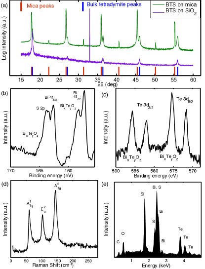
X-ray diffraction (XRD) spectra of as-grown BTS-on-SiO2 and BTS-on-mica samples show evidence of particularly c-axis oriented growth, i.e., sharp peaks only at the positions of the (0 0 n) facet reflections of the bulk tetradymite crystalGlatz (1967); Downs and Hall-Wallace (2003); Ji et al. (2012), as seen from Fig-2(a). The AFM and XRD results confirm that, once nucleated, the BTS nanosheets subsequently grow epitaxially, forming the layered van der Waals crystal structure of the tetradymite. Raman spectra show sharp peaks (see Fig-2(d)), which are coincident with tetradymite spectrumDowns and Hall-Wallace (2003); Chis et al. (2012). Major Raman shifts are observed at A cm-1, E cm-1 and A cm-1, which when compared to Bi2Te3, exhibit a blue shift. The S-atoms occupy the middle chalcogen layer and intermix with Te-atoms in the outer chalcogen layers in the BTS crystalPauling (1975); Ji et al. (2012). Replacing the Te atoms in the Bi2Te3 unit cell with the smaller S atoms leads to a smaller BiS bond length, more compressive strain and non-stoichiometry in the ideal tetradymite lattice, leading to the so called -phase in the temperature range of the growth ()Glatz (1967); Pauling (1975); Ji et al. (2012). The compressive strain leads to the blue shift observed in the Raman spectrumChis et al. (2012). Core-level X-ray photoelectron spectroscopy (XPS) analysis on candidate BTS samples show the presence of the expected Bi 4f, S 2p and Te 3d bonding states, shown in Fig-2(b) and (c)Roy et al. (2013); Purkayastha et al. (2008); Aminorroaya-Yamini et al. (2012). The chemical shifts at higher bonding energies away from the Bi 4f states point to the presence of a surface oxide, as do the ones observed for the Te 3d statesPurkayastha et al. (2008), justifying the need for plasma treating the surface of the BTS nanosheets before contact metal deposition during device fabrication. Energy dispersive X-ray spectroscopy on candidate BTS nanosheets on SiO2 and mica show the presence of Bi, Te and S in all samples (see Fig-2(e)) and stoichiometries are established in the range of Bi2Te2-xS1+x with , in near agreement with the -phase, the proposed alternative to the ideal structure of the tetradymiteGlatz (1967); Pauling (1975); Soonpaa (1962).
III.2 Temperature-dependent Conductivity Measurements
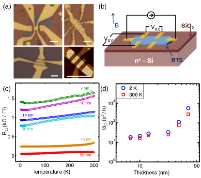
Some examples of devices fabricated on as-grown BTS nanosheets on SiO2 substrates in a four-point or Hallbar geometry, are shown in Fig-3(a). All measurements were done in the constant current mode, as shown in the representative schematic in Fig-3(b). Four-point resistance was measured as a function of the sample temperature, showing an almost linearly decreasing resistance for all devices (see Fig-3(c)). This is indicative of a doped bulk, likely due to chalcogen deficiencies (donors) and antisite defects (acceptors), characteristic of Bi-chalcogenide TI materialsWang et al. (2013). The BTS devices were found to be dominantly n-type from Hall data. Due to a vapor pressure higher than Tellurium, Sulfur evaporates more during growth and device processing leaving behind donor vacancies, while the Bi-S bonding in BTS reduces acceptor-like antisite defect formation, leading to an overall n-type behaviorJi et al. (2012). This observation was also made for the bulk crystal case in previous experimentsSoonpaa (1962); Ji et al. (2012). Care must thus be taken to reduce the overall fabrication and processing temperature, as was done in this study. Interestingly, a previous experiment on non-stoichiometric BTS bulk crystals also showed highly anisotropic conductance, i.e., the ratio of in-plane (, perpendicular to the c-axis of the crystal) to out-of-plane (, parallel to the c-axis of the crystal) conductivity was largeSoonpaa (1962). Sheet conductance data for several BTS devices are also plotted vs the BTS nanosheet thickness in Fig-3(d). is approximately flat for thinner devices, which indicates the large contribution of the surface channel to the sample conductanceHe et al. (2011); Bansal et al. (2012). As increases, a corresponding increase in is seen, not unlike a doped semiconductor. This increase in conductivity indicates the growing contribution of the bulk channel for thicker nanosheets, which has been explained as increased impurity band statesHe et al. (2011).
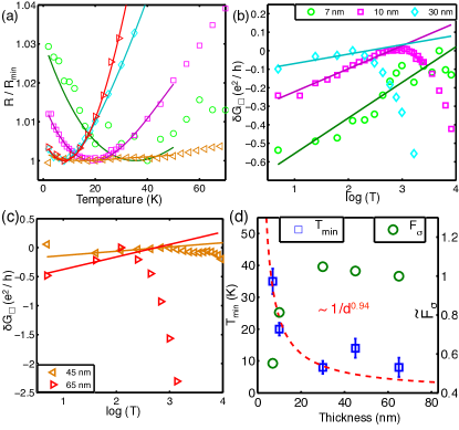
There is a decrease in the rate of reduction of resistance at lower temperatures ( K), oftentimes showing an increase in the resistance (see Fig-4(a)), or a decrease in conductivity. This decrease in the conductivity is linearly proportional to logarithmic temperature and is indicative of an insulating ground state, expected for a 2D system with electron-electron interaction (EEI), in which the Coulomb interaction between electrons is enhanced and becomes long rangeLee and Ramakrishnan (1985); Altshuler and Aronov (1985); Liu et al. (2011); Wang et al. (2011); Lu and Shen (2014). The correction to the conductivity due to the dynamically screened interaction can be expressed asLee and Ramakrishnan (1985); Beutler and Giordano (1988):
| (1) |
Where the fitting parameter is a Hartree term related to the strength of Coulomb screening and is a reference characteristic temperature, taken as 2 K for this experimentLee and Ramakrishnan (1985); Beutler and Giordano (1988). Example fits for the different BTS devices are shown in Fig-4(b) and (c). Incidentally, the conductivity for the nm device was observed to flatten out at low temperatures, unlike other devices that show a decrease, and hence could not be fitted to the EEI model. The likely reason for this observation is that out of the competing contributions from WAL and EEI, the WAL contribution is larger than EEI for the 14 nm device, and hence the decrease in conductivity due to EEI is smaller than that observed for other devices. The competing contributions are discussed in more detail in Section III.4. The exact definition of the fit parameter depends on the dimensionality of the sample, which for two-dimensional films is: , where is the dimensionless interaction averaged on the Fermi surface, and for values of within Lee and Ramakrishnan (1985). The nature and values of the screening parameter are a matter of some debate due to the immense difficulty involved in its exact calculation and variance in experimental observationLee and Ramakrishnan (1985); Altshuler and Aronov (1985); Lin et al. (2001); Chen et al. (2011); Takagaki et al. (2012b). However, qualitatively from the Thomas-Fermi theory the values of from to signify weaker screening (larger correction) to stronger screening (smaller correction) for most metals in presence of disorderLin et al. (2001); Lu and Shen (2014). The values of from the EEI fits are shown in 4(d) as a function of nanosheet thickness, going from a value of for thinner to for thicker devices. These values indicate stronger screening in thicker devices, likely due to larger contribution from bulk carriers to the transport, thus leading to a smaller correction to Lu and Shen (2014). Similar values in this range have been reported for devices of TI materials and thin films of strong spin-orbit coupling materials, such as elemental BiAltshuler and Aronov (1985); McLachlan (1983); Woerlee, Verkade, and Jansen (1983); Liu et al. (2011); Wang et al. (2011); Chen et al. (2011); Lu and Shen (2014). The temperatures , when , are plotted vs thickness () of the BTS nanosheet in Fig-4(d) showing a fit. This behavior of can be derived from a conduction model considering both surface and bulk channels contributing to the total transport (see Appendix A for derivation). The decreasing vs data are qualitatively similar to the observation made for the sheet conductance vs , as the bulk channels become more dominant for thicker devices and the onset of the 2D interaction-driven ground state is evident at lower temperatures.
III.3 Thickness-dependent Magnetotransport Measurements
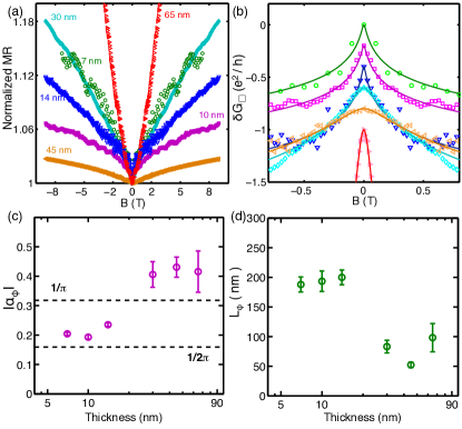
The symmetric longitudinal magnetoresistance (MR) in perpendicular magnetic field is shown in Fig-5(a) for several BTS devices of different thicknesses. The MR shows a sharp cusp in low-field range, which is representative of weak antilocalization (WAL). It is a result of the negative interference in electron paths due to Berry’s phase in TIsFu and Kane (2007). The WAL effect is especially an indicator of topologically protected surface states as TIs belong to the symplectic class and unlike topologically trivial 2D systems, don’t show a crossover to weak localization from WALChen et al. (2010). Incidentally, fluctuations in the MR are also evident for thinner devices, which will be addressed later. The WAL correction to the conductivity has been computed by Hikami, Larkin and Nagaoka (HLN), and for the symplectic case it isHikami, Larkin, and Nagaoka (1980):
| (2) |
Prefactor in Eq-2 is indicative of the nature and number of conduction channels and is the dephasing field, associated with the characteristic phase decoherence length . Eq-2 is a simplified or reduced version of the full HLN conductivity correction, assuming strong spin orbit coupling in the transport direction, no magnetic scattering and large elastic scattering timeHikami, Larkin, and Nagaoka (1980). is exactly equal to for the symplectic case of the 2D topological surface channel. Several of the device MR data are fitted to Eq-2 in low-field limit to extract and , as shown in Fig-5(b). As can be seen from Fig-5(c) for thinner devices and for thicker ones it is larger than . The exact meaning of the values and trends of the prefactor has been a matter of some debate, and because of its empirical fitting nature it is more an indirect indicator of the underlying complex picture of multi-channel transportChen et al. (2010); Steinberg et al. (2011); Chen et al. (2011); Lee et al. (2012); Xia et al. (2013); Kim et al. (2013). Qualitatively however, one can distinguish regimes of transport: can almost continuously vary from an ideal picture of parallel symplectic channels, i.e., surface states (), to a more complicated picture of surface states coupled via conductive bulk (non-integer multiples of ). Value of has been attributed to phase-preserving coherent scattering between the two surface states and bulk states, which are only partially decoupled such that the contribution effectively adds up to less than two full channelsSteinberg et al. (2011); Chen et al. (2011); Li et al. (2012); Kim et al. (2013); Yang et al. (2014). Similarly, may indicate a larger degree of separation of surfaces but with an addition of other channels: larger bulk contribution in thicker devices and trivial 2D subbands, occurring mainly due to surface band bendingBianchi et al. (2010); Lee et al. (2012); Yang et al. (2014). This observation corroborates the vs data from Fig-3(d). The argument is further supported by the phase coherence length data, as shown in Fig-5(d) where is larger for thinner devices. This may be explained as a lower (higher) bulk channel contribution and hence a lower (higher) surface-to-bulk scattering in thinner (thicker) devices leading to a longer (shorter) phase-coherence time and lengthSteinberg et al. (2011).
III.4 Temperature-dependent Magnetotransport Measurements
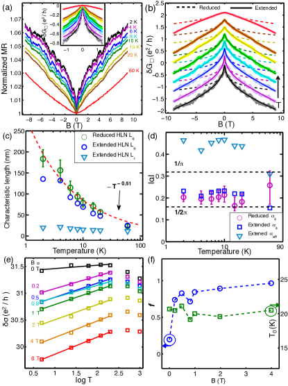
Temperature-dependent magnetoresistance measurement results for a candidate thin BTS device ( nm) are shown in Fig-6. The MR shows a sharp WAL cusp (Fig-6(a)), which gets smaller as the sample temperature increases. The solid lines in Fig-6(a) inset show the reduced HLN fits to the magnetoconductance at low magnetic fields. The limitation of the reduced fit is apparent if it is expanded to include full-range MR data (dashed lines in Fig-6(b)), as the high-field magnetoconductivity is not dominated by the quantum-only correction of Eq-2 unlike in the low-field case.
We have considered an extended version of the HLN equation as an alternative, with added terms:
| (3) |
Eq-3 has two extra correction terms compared to Eq-2. The second term is similar to the first in form, but it represents the contribution from elastic scatteringHikami, Larkin, and Nagaoka (1980); Zhang et al. (2012); Dey et al. (2014). The prefactor is an indicator of multiple channels effectively contributing to the correction. The final term is the conventional quadratic cyclotron term, which provides a negative correction to the overall conductivityAssaf et al. (2013); Shekhar et al. (2014). The extended HLN fit of Eq-3 proves more reliable for full-range fitting (solid lines in Fig-6(b)). The characteristic lengths associated with the two dephasing fields in Eq-3, and the reduced HLN , are shown as a function of temperature in Fig-6(c) matching closely. The dashed line represents a dependence, which is an attribute of a 2D system and corresponds to Nyquist electron-electron decoherenceAltshuler, Aronov, and Khmelnitsky (1982); Lee et al. (2012); Dey et al. (2014). The elastic scattering length and changes relatively little over the temperature range. v from both the fits are shown in Fig-6(d) matching relatively well. The equivalent prefactor of the surface channel in the extended HLN fit is obtained from the effective prefactor as . As before, is slightly larger than at lower temperatures for both fits, indicating the presence of mainly a symplectic 2D channel, partially decoupled with the bulk states, contributing to the WAL. It is also instructive to consider the value of , which is . A value larger than unity indicates the presence of more than one channel contributingLee et al. (2012), especially with the elastic scattering term in Eq-3. The data at 60K is almost parabolic with a very small WAL feature, such that the first and second terms in Eq-3 act equivalently for the purposes of the fit and gives larger error in the reduced HLN case. The fitting parameter can be expressed as , where is the mobility estimated from the parabolic MR term and for isotropic scattering should be approximately similar to Schroder (2006). The from the fit is very close to the Hall mobility (Fig-7(b)), i.e., cm2/Vs. The temperature-dependent 2D behavior of and the values of can be understood as arising from topological surface channel contributing to the WAL cusp, while the conductive bulk also contributes to the high-field MR behavior. In prior study on Bi2Te3 films, additional conductivity correction terms in the HLN equation from spin-orbit scattering, were also consideredZhang et al. (2012); Dey et al. (2014). However, for our data the spin-orbit dephasing fields , hence could be safely ignored from the fit. The contribution from the WAL effect dominates the conductivity at low-temperatures and at zero-field. The expected quantum correction to the temperature-dependent conductivity in disordered systems due to localization is (in units of ):
| (4) |
Where the phase coherence time ( for 2D), is a prefactor similar in nature to from the HLN fit and is the temperature at which the correction disappearsBeutler and Giordano (1988); Takagaki et al. (2012b); Lu and Shen (2014). The conductivity should continue to increase with decreasing temperature for a purely WAL-like contribution. However, as discussed in Section III.2, the devices show a decrease in the conductivity with decreasing temperature, which is linearly proportional to logarithmic temperature and is attributed to EEI. The EEI correction is also logarithmic in nature similar to Eq-4, as seen from Eq-1. The low-temperature conductivity in different perpendicular magnetic fields can be then fitted to a generic equation of the form (in units of ):
| (5) |
Where is the slope of the line (equivalent to , from Eq-4 and Eq-1) and is the characteristic temperature. Fig-6(e) shows the temperature dependent conductivity fits to Eq-5, and Fig-6(f) shows the values of as a function of magnetic field. saturates to at fields higher than T, whereas is within K and approximately independent of field. Thus the WAL and EEI effects arise in a similar temperature range. The value of can be extracted from with for 2D states, which is slightly different than the HLN-fitted but still indicates effectively a single surface state with a bulk contributionLiu et al. (2011); Lu and Shen (2014). This variation in has been observed in previous experimentsBeutler and Giordano (1988); Wang et al. (2011); Takagaki et al. (2012b); Roy et al. (2013); Lu and Shen (2014). The saturating value of at higher fields points to a dominant contribution from EEI, as the magnetic field dependence of EEI is weaker, while the low-field variation in may be attributed to the WAL effect, such as both effects act in combination for the BTS devicesBeutler and Giordano (1988); Takagaki et al. (2012b, a); Roy et al. (2013); Lu and Shen (2014).
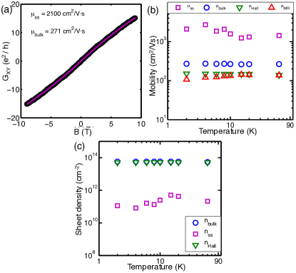
Fig-7 shows the results obtained from a two-channel modelRen et al. (2010); Steinberg et al. (2010); Bansal et al. (2012); Yang et al. (2014) fit to the Hall conductivity data, to investigate the parallel contribution from the surface and bulk effective channels (see Appendix B for details). Fig-7(a) shows the two-channel fit to the Hall conductivity data for the 10 nm BTS device. The two mobilities and carrier densities extracted from the model fit are shown in Fig-7(b) and (c), respectively, compared with the values computed directly from the Hall coefficient. The bulk carrier concentrations from both Hall and two-channel models are close to previously reported carrier densities for bulk crystals showing n-type dopingSoonpaa (1962); Ji et al. (2012). The two-channel model reveals the presence of a higher mobility and lower carrier density surface channel, i.e., , whereas the lower mobility and higher carrier density channel, , is indicative of an effective contribution from the bulk channel. The two-channel model fits the data well up to higher temperatures, where the surface state channel is still found to contribute to the overall conduction, with the bulk conduction states always present.
III.5 Universal Conductance Fluctuations
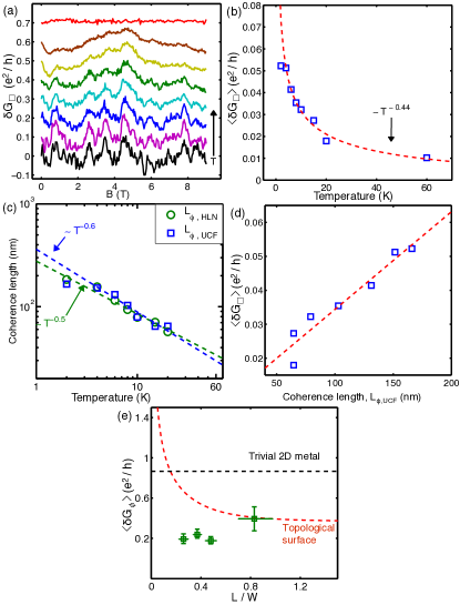
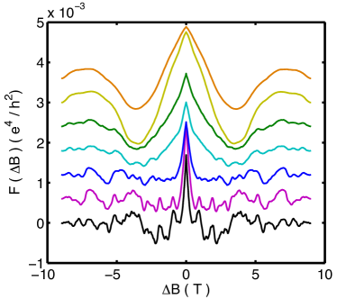
Fluctuations in the magnetoresistance are evident for thinner devices, for example in the 10 nm device in Fig-6(a) and can be visualized better by subtracting the smooth background from the extended HLN fits (Fig-8(a)), seen to be persisting up to higher temperatures. Universal conductance fluctuations (UCF) are a manifestation of an electron’s path interfering with itself, as it goes around a defect site. If the phase of the electron is preserved over a mesoscopic scale , then the interference leads to measurable variance or fluctuations in the conductance. When the sample dimensions are larger than there is some self-averaging due to changing impurity potential configurationAl’tshuler and Khmel’nitskii (1985); Lee, Stone, and Fukuyama (1987), which can reduce the overall amplitude of the fluctuations. To calculate the amplitude, a correlation function of the fluctuations is calculated asLee, Stone, and Fukuyama (1987): , where (see Appendix C for examples of the correlation function). The UCF magnitude is obtained at and is of the order of , decaying as from our experimental data (Fig-8(c)). This temperature dependence is similar to theoretically expected dependence in a 2D systemAl’tshuler and Khmel’nitskii (1985); Lee, Stone, and Fukuyama (1987); Lee et al. (2012); Li et al. (2012); Xia et al. (2013). The correlation-field (related to the scale of the UCF) can be calculated from the correlation function as and the related phase coherence length as , where is the flux quantumLee, Stone, and Fukuyama (1987). As seen in Fig-8(c) matches closely with and decays as , which confirms that the fluctuations are primarily from the 2D surface channelLee, Stone, and Fukuyama (1987). Also expected from 2D UCF theory is the linear relation of rms value of the fluctuations with the corresponding phase coherence lengthLee, Stone, and Fukuyama (1987); Gehring et al. (2013) (see Fig-8(d)). To see the consequence of finite size effects on the UCF magnitudes, devices of different dimensions () can be compared for their rms values. For a true comparison the rms value of the UCF within a phase-coherent box should be considered, which calculated as , where is the number of phase coherent boxes in a samplePal, Kochat, and Ghosh (2012). Rossi et al. have proposed an approach to compare UCF amplitudes in Dirac materials, independent of impurity density, disorder strength and correlation lengthRossi et al. (2012):
| (6) |
In Eq-6 the spin and valley degeneracies for TI surface channel is Rossi et al. (2012). Fig-8(e) shows the phase coherent UCF magnitudes of several devices as a function of the dimensional ratio . The red dotted line shows the behavior of a topological surface channel from Eq-6; the black dotted line is the expected value of the UCF magnitude () for a topologically trivial 2D-electron gas (2DEG)Al’tshuler (1985); Li et al. (2014). The UCF magnitudes are somewhat less than the magnitude expected from topological states according to Eq-6, but they are much less than trivial 2D metal values, indicating that the conductivity fluctuations largely arise due to the topological surface statesLi et al. (2014); Gehring et al. (2015).
IV Conclusions
In summary, we demonstrate van der Waals epitaxial growth of crystalline Bismuth Telluro-Sulfide (BTS) nanosheets on SiO2 and mica substrates. As grown BTS material is obtained in highly layered, good-quality crystalline nanosheets. Detailed transport experiments in devices of BTS indicate the presence of surface states, albeit with bulk states still present in the transport. Weak anti-localization and universal conductance fluctuation signatures are seen in the magnetoresistance of the BTS devices. Evidence of a combination of both weak antilocalization and electron-electron interaction effects is seen from analyzing the insulating ground state in the temperature and field-dependent conductivity data. An extended-HLN model is considered, which provides excellent fitting to longitudinal magnetoconductance data in high-field range, and indicates the presence of 2D surface states, partially coupled to the bulk conducting states. Two-channel Hall conductivity model in conjunction with the extended-HLN model provides a good fit for the magnetoconductance data. The HLN effective prefactor provides a good qualitative tool to understand the regimes of transport in the device, and its value is indicative of the contribution of different channels acting in parallel. Universal conductance fluctuations are observed in thin BTS devices. The temperature dependent phase coherence lengths from UCF data are in reasonable agreement with those from WAL data, showing 2D behavior arising from topological surface states. The magnetoconductivity data and its empirical modeling show that the bulk conduction channels are still present in the BTS material, likely due to high level of n-type doping by chalcogen deficiency. Our studies confirm BTS as a candidate 3D TI material in conjunction with the previous APRES measurements, and takes a step closer to understanding transport mechanism in TI materials. Future growth experiments of the BTS material on highly crystalline substrates and substitutional doping with more p-type elements such as Sb, are expected to improve the electronic properties of the BTS material system by reducing the chalcogen deficiency doping and pushing the Fermi level further into the bandgap, leading to the predicted promising nature of the Sulfur based ternary tetradymite. Additionally, more experiments with top and bottom gating on high-quality BTS material are also expected to reveal further the nature and contribution of the multiple transport channels acting in parallel in 3D TIs. BTS provides an alternative material with surface-states accessible by transport measurements, to further probe the topological nature of the states and for potential heterostructure-based applications of different 3D TIs in nanoelectronics.
Acknowledgements.
This work was supported in part by the Nanoelectronics Research Initiative’s (NRI) South West Academy of Nanoelectronics (SWAN) and the National Nanotechnology Coordinated Infrastructure (NNCI). T.T. thanks Kyounghwan Kim for helping to build and troubleshoot the growth system, Dr. Anupam Roy and Rik Dey for valuable discussions and Dr. Babak Fallahazad for helping with wirebonding.Appendix A Electron-electron Interaction Driven Insulating Ground State
The sheet resistance of the BTS devices shows indications of an insulating ground state, as observed in the main text. Oftentimes, the insulating ground state manifests as an increase (decrease) in the sheet resistance (conductance) as the sample is further cooled down. The correction to the conductivity due to the electron-electron interaction (EEI) effects in 2D systems is given by Eq-1 in the main text. The temperature dependent conductance data of several BTS devices fit the linear expression of Eq-1 in , as seen from Fig-4. Assuming that the total conductivity can be represented as a sum of effectively two types of contribution, i.e., surface and bulk channelsSteinberg et al. (2010); Ren et al. (2010):
| (7) |
Where and are the total conductivity, bulk conductivity and surface state (SS) conductance, respectively. Assuming that the bulk conductivity component is largely independent of the thickness of the film, and that the SS conductance follows the 2D EEI relation of Eq-7 (up to some correction factor converting between conductance and conductivity), a temperature-dependent conductivity correction can be written as:
| (8) |
in Eq-8 is a combined constant factor of all the temperature independent variables obtained after differentiating the expression in Eq-7 and Eq-1. As can be seen from Eq-8, the temperature of the resistance minima (or conductivity maxima) scale roughly as . This thickness dependent behavior is noted in the main text for BTS devices, where a fit is obtained for the experimentally observed for several devices.
Appendix B Two-channel Model
A two-channel model is widely used to fit Hall conductance data in TI devices, as also utilized in Appendix ARen et al. (2010); Steinberg et al. (2010); Bansal et al. (2012). Fig-7 in main text shows an example two-channel fit to a candidate device ( nm). A generic multi-carrier model can be represented as:
| (9) |
Where are the carrier concentration and mobility of the channel, respectively. are the conductance tensor components. With some basic algebra and limiting assumptions the number of unknown variables in the fit can be reduced and the following equation can be used for a two-channel modelBansal et al. (2012):
Appendix C Universal Conductance Fluctuations Correlation Function
The magnitude of the conductance fluctuations and the correlation field can be calculated from the correlation function, in a device exhibiting UCF in the magnetoresistance. The correlation function can be calculated as: , where . Examples of the correlation function for a candidate device (10 nm) are shown in Fig-9.
References
- Fu and Kane (2007) L. Fu and C. L. Kane, Physical Review B 76, 045302 (2007).
- Hasan and Kane (2010) M. Z. Hasan and C. L. Kane, Reviews of Modern Physics 82, 3045 (2010).
- Ando (2013) Y. Ando, Journal of the Physical Society of Japan 82, 102001 (2013).
- Pesin and MacDonald (2012) D. Pesin and A. H. MacDonald, Nature Materials 11, 409 (2012).
- Li et al. (2010) R. Li, J. Wang, X.-L. Qi, and S.-C. Zhang, Nature Physics 6, 284 (2010).
- Chen et al. (2010) J. Chen, H. J. Qin, F. Yang, J. Liu, T. Guan, F. M. Qu, G. H. Zhang, J. R. Shi, X. C. Xie, C. L. Yang, K. H. Wu, Y. Q. Li, and L. Lu, Physical Review Letters 105, 176602 (2010).
- Steinberg et al. (2010) H. Steinberg, D. R. Gardner, Y. S. Lee, and P. Jarillo-Herrero, Nano Letters 10, 5032 (2010).
- He et al. (2011) L. He, F. Xiu, Y. Wang, A. V. Fedorov, G. Huang, X. Kou, M. Lang, W. P. Beyermann, J. Zou, and K. L. Wang, Journal of Applied Physics 109, 103702 (2011).
- Wang et al. (2011) J. Wang, A. M. DaSilva, C.-Z. Chang, K. He, J. K. Jain, N. Samarth, X.-C. Ma, Q.-K. Xue, and M. H. W. Chan, Physical Review B 83, 245438 (2011).
- Liu et al. (2011) M. Liu, C.-Z. Chang, Z. Zhang, Y. Zhang, W. Ruan, K. He, L.-l. Wang, X. Chen, J.-F. Jia, S.-C. Zhang, Q.-K. Xue, X. Ma, and Y. Wang, Physical Review B 83, 165440 (2011).
- Chen et al. (2011) J. Chen, X. Y. He, K. H. Wu, Z. Q. Ji, L. Lu, J. R. Shi, J. H. Smet, and Y. Q. Li, Physical Review B 83, 241304 (2011).
- Steinberg et al. (2011) H. Steinberg, J.-B. Laloë, V. Fatemi, J. S. Moodera, and P. Jarillo-Herrero, Physical Review B 84, 233101 (2011).
- Bansal et al. (2012) N. Bansal, Y. S. Kim, M. Brahlek, E. Edrey, and S. Oh, Physical Review Letters 109, 116804 (2012).
- Taskin et al. (2012) A. A. Taskin, S. Sasaki, K. Segawa, and Y. Ando, Physical Review Letters 109, 066803 (2012).
- Takagaki et al. (2012a) Y. Takagaki, A. Giussani, K. Perumal, R. Calarco, and K.-J. Friedland, Physical Review B 86, 125137 (2012a).
- Roy et al. (2013) A. Roy, S. Guchhait, S. Sonde, R. Dey, T. Pramanik, A. Rai, H. C. P. Movva, L. Colombo, and S. K. Banerjee, Applied Physics Letters 102, 163118 (2013).
- Lee et al. (2012) J. Lee, J. Park, J.-H. Lee, J. S. Kim, and H.-J. Lee, Physical Review B 86, 245321 (2012).
- Kim et al. (2013) D. Kim, P. Syers, N. P. Butch, J. Paglione, and M. S. Fuhrer, Nature Communications 4, 2040 (2013).
- Yang et al. (2014) F. Yang, A. A. Taskin, S. Sasaki, K. Segawa, Y. Ohno, K. Matsumoto, and Y. Ando, Applied Physics Letters 104, 161614 (2014).
- Ren et al. (2010) Z. Ren, A. A. Taskin, S. Sasaki, K. Segawa, and Y. Ando, Physical Review B 82, 241306 (2010).
- Wang and Johnson (2011) L.-L. Wang and D. D. Johnson, Physical Review B 83, 241309 (2011).
- Kong et al. (2011) D. Kong, Y. Chen, J. J. Cha, Q. Zhang, J. G. Analytis, K. Lai, Z. Liu, S. S. Hong, K. J. Koski, S.-K. Mo, Z. Hussain, I. R. Fisher, Z.-X. Shen, and Y. Cui, Nature Nanotechnology 6, 705 (2011).
- Xia et al. (2013) B. Xia, P. Ren, A. Sulaev, P. Liu, S.-Q. Shen, and L. Wang, Phys. Rev. B 87, 085442 (2013).
- Soonpaa (1962) H. H. Soonpaa, Journal of Applied Physics 33, 2542 (1962).
- Glatz (1967) A. C. Glatz, The American Mineralogist 52, 161 (1967).
- Pauling (1975) L. Pauling, The American Mineralogist 60, 994 (1975).
- Ji et al. (2012) H. Ji, J. M. Allred, M. K. Fuccillo, M. E. Charles, M. Neupane, L. A. Wray, M. Z. Hasan, and R. J. Cava, Physical Review B 85, 201103 (2012).
- Takagaki et al. (2011) Y. Takagaki, B. Jenichen, U. Jahn, M. Ramsteiner, K. Friedland, and J. Lähnemann, Semiconductor Science and Technology 26, 125009 (2011).
- Koma (1999) A. Koma, Journal of Crystal Growth 201 -202, 236 (1999).
- Ferhat et al. (1996) M. Ferhat, B. Liautard, G. Brun, J. Tedenac, M. Nouaoura, and L. Lassabatere, Journal of Crystal Growth 167, 122 (1996).
- Hao et al. (2012) G. Hao, X. Qi, Y. Liu, Z. Huang, H. Li, K. Huang, J. Li, L. Yang, and J. Zhong, Journal of Applied Physics 111, 114312 (2012).
- Peng et al. (2012) H. Peng, W. Dang, J. Cao, Y. Chen, D. Wu, W. Zheng, H. Li, Z.-X. Shen, and Z. Liu, Nature Chemistry 4, 281 (2012).
- Gehring et al. (2012) P. Gehring, B. F. Gao, M. Burghard, and K. Kern, Nano Letters 12, 5137 (2012).
- Dang et al. (2010) W. Dang, H. Peng, H. Li, P. Wang, and Z. Liu, Nano Letters 10, 2870 (2010).
- Michely et al. (1993) T. Michely, M. Hohage, M. Bott, and G. Comsa, Physical Review Letters 70, 3943 (1993).
- Roy et al. (2015) A. Roy, S. Guchhait, R. Dey, T. Pramanik, C.-C. Hsieh, A. Rai, and S. K. Banerjee, ACS Nano 9, 3772 (2015).
- Liu et al. (1993) S. Liu, Z. Zhang, G. Comsa, and H. Metiu, Physical Review Letters 71, 2967 (1993).
- Downs and Hall-Wallace (2003) R. T. Downs and M. Hall-Wallace, The American Mineralogist 88, 247 (2003).
- Chis et al. (2012) V. Chis, I. Y. Sklyadneva, K. A. Kokh, V. A. Volodin, O. E. Tereshchenko, and E. V. Chulkov, Physical Review B 86, 174304 (2012).
- Purkayastha et al. (2008) A. Purkayastha, Q. Yan, M. S. Raghuveer, D. D. Gandhi, H. Li, Z. W. Liu, R. V. Ramanujan, T. Borca-Tasciuc, and G. Ramanath, Advanced Materials 20, 2679 (2008).
- Aminorroaya-Yamini et al. (2012) S. Aminorroaya-Yamini, C. Zhang, X. Wang, and I. Nevirkovets, Journal of Physics D: Applied Physics 45, 125301 (2012).
- Wang et al. (2013) L.-L. Wang, M. Huang, S. Thimmaiah, A. Alam, S. L. Bud’ko, A. Kaminski, T. A. Lograsso, P. Canfield, and D. D. Johnson, Physical Review B 87, 125303 (2013).
- Lee and Ramakrishnan (1985) P. A. Lee and T. V. Ramakrishnan, Reviews of Modern Physics 57, 287 (1985).
- Altshuler and Aronov (1985) B. L. Altshuler and A. G. Aronov, Electron-Electron Interactions in Disordered Systems, edited by A. L. Efros and M. Pollak, Modern Problems in Condensed Matter Sciences, Vol. 10 (Elsevier, Amsterdam, 1985).
- Lu and Shen (2014) H.-Z. Lu and S.-Q. Shen, Physical Review Letters 112, 146601 (2014).
- Beutler and Giordano (1988) D. E. Beutler and N. Giordano, Physical Review B 38, 8 (1988).
- Lin et al. (2001) J. J. Lin, S. Y. Hsu, J. C. Lue, and P. J. Sheng, Journal of Physics and Chemistry of Solids 62, 1813 (2001).
- Takagaki et al. (2012b) Y. Takagaki, B. Jenichen, U. Jahn, M. Ramsteiner, and K.-J. Friedland, Physical Review B 85, 115314 (2012b).
- McLachlan (1983) D. S. McLachlan, Physical Review B 28, 6821 (1983).
- Woerlee, Verkade, and Jansen (1983) P. H. Woerlee, G. C. Verkade, and A. G. M. Jansen, Journal of Physics C: Solid State Physics 16, 3011 (1983).
- Hikami, Larkin, and Nagaoka (1980) S. Hikami, A. I. Larkin, and Y. Nagaoka, Progress of Theoretical Physics 63, 707 (1980).
- Li et al. (2012) Z. Li, T. Chen, H. Pan, F. Song, B. Wang, J. Han, Y. Qin, X. Wang, R. Zhang, J. Wan, D. Xing, and G. Wang, Scientific Reports 2, 595 (2012).
- Bianchi et al. (2010) M. Bianchi, D. Guan, S. Bao, J. Mi, B. B. Iversen, P. D. C. King, and P. Hofmann, Nature Communications 1, 128 (2010).
- Zhang et al. (2012) S. X. Zhang, R. D. McDonald, A. Shekhter, Z. X. Bi, Y. Li, Q. X. Jia, and S. T. Picraux, Applied Physics Letters 101, 202403 (2012).
- Dey et al. (2014) R. Dey, T. Pramanik, A. Roy, A. Rai, S. Guchhait, S. Sonde, H. C. P. Movva, L. Colombo, L. F. Register, and S. K. Banerjee, Applied Physics Letters 104, 223111 (2014).
- Assaf et al. (2013) B. A. Assaf, T. Cardinal, P. Wei, F. Katmis, J. S. Moodera, and D. Heiman, Applied Physics Letters 102, 012102 (2013).
- Shekhar et al. (2014) C. Shekhar, C. E. ViolBarbosa, B. Yan, S. Ouardi, W. Schnelle, G. H. Fecher, and C. Felser, Phys. Rev. B 90, 165140 (2014).
- Altshuler, Aronov, and Khmelnitsky (1982) B. L. Altshuler, A. G. Aronov, and D. E. Khmelnitsky, Journal of Physics C: Solid State Physics 15, 7367 (1982).
- Schroder (2006) D. K. Schroder, Semiconductor Material and Device Characterization, 3rd ed. (Wiley-IEEE Press, 2006).
- Al’tshuler and Khmel’nitskii (1985) B. Al’tshuler and D. Khmel’nitskii, JETP Letters 42, 291 (1985).
- Lee, Stone, and Fukuyama (1987) P. A. Lee, A. D. Stone, and H. Fukuyama, Physical Review B 35, 1039 (1987).
- Gehring et al. (2013) P. Gehring, H. M. Benia, Y. Weng, R. Dinnebier, C. R. Ast, M. Burghard, and K. Kern, Nano Letters 13, 1179 (2013).
- Pal, Kochat, and Ghosh (2012) A. N. Pal, V. Kochat, and A. Ghosh, Physical Review Letters 109, 196601 (2012).
- Rossi et al. (2012) E. Rossi, J. H. Bardarson, M. S. Fuhrer, and S. Das Sarma, Physical Review Letters 109, 096801 (2012).
- Al’tshuler (1985) B. Al’tshuler, JETP Letters 41, 648 (1985).
- Li et al. (2014) Z. Li, Y. Meng, J. Pan, T. Chen, X. Hong, S. Li, X. Wang, F. Song, and B. Wang, Applied Physics Express 7, 065202 (2014).
- Gehring et al. (2015) P. Gehring, K. Vaklinova, A. Hoyer, H. M. Benia, V. Skakalova, G. Argentero, F. Eder, J. C. Meyer, M. Burghard, and K. Kern, Scientific Reports 5, 11691 (2015).