Design and fabrication of diffractive atom chips for laser cooling and trapping
Abstract
It has recently been shown that optical reflection gratings fabricated directly into an atom chip provide a simple and effective way to trap and cool substantial clouds of atoms nshii13 ; mcgilligan15 . In this article we describe how the gratings are designed and micro-fabricated and we characterise their optical properties, which determine their effectiveness as a cold atom source. We use simple scalar diffraction theory to understand how the morphology of the gratings determines the power in the diffracted beams.
1 Introduction
Atom chips are microfabricated devices which control and manipulate ultracold atoms in a small, integrated package. Because they provide a convenient way to trap lewis09 ; pollock09 ; pollock11 , guide hinds99 ; dekker00 and detect atoms eriksson05 , atom chips are becoming increasingly important for clocks treutlein04 , Bose-Einstein condensates hansel01 ; ott01 , matter wave interferometers schumm05 ; pollock09 ; baumgartner10 , and quantum metrology riedel10 . In recent years there has been great progress towards integrating a wide range of optical, electric and magnetic elements into atom chips, but the magneto-optical trap (MOT) lindquist92 ; reichel99 - the element responsible for initial capture and cooling of the atoms - has remained external to the chip.
Following lee96 , an early attempt to integrate the MOT used deep pyramidal mirrors etched into a thick silicon substrate. These manipulate a single incident laser beam into the overlapping beams required by a MOT. With beams of small size , the number of atoms captured scales as pollock11 , a dependence that rolls over to as the size increases to some centimeters lindquist92 . The large pyramids favoured by this scaling are not compatible with the normal m thickness of a silicon wafer. Although thick wafers are available, days of etching are needed to make pyramids of mm size and additional polishing is required to achieve optical quality surfaces pollock09 ; laliotis12 ; cotter13 . For these reasons the integrated pyramid is unsuitable for applications requiring more than atoms. Fig. 1 illustrates a recent extension of this idea where the MOT beams are now formed using microfabricated diffraction gratings, which replace the sloping walls of the pyramid vangeleyn09 ; vangeleyn10 . The gratings are easily fabricated on any standard substrate material, and can readily be made on the centimeter scale. This allows the MOT to capture up to atoms above the surface of the chip, where they can be conveniently transferred to magnetic traps hinds99 . Because they only need a small depth of etching, the gratings preserve the D nature of the structure and sit comfortably with other elements on the chip. Alternatively, for devices that only require the reliable production of a MOT, the grating chip can be placed outside the wall of a glass cell and used to trap atoms on the inside.
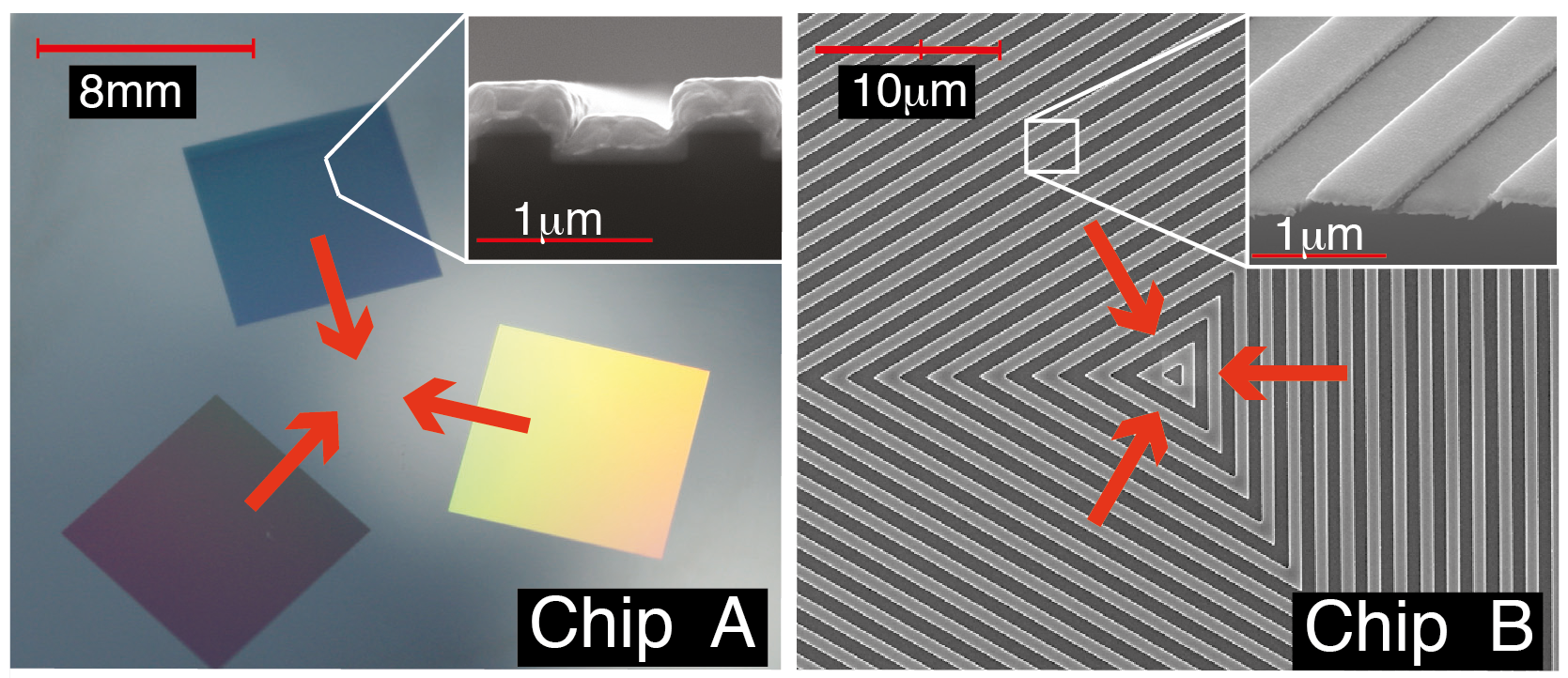
Figure 2 shows two 1D-grating MOT chips which have already been demonstrated nshii13 . Chip A has three square grating areas arranged symmetrically to leave a plane area in the centre. Chip B has the same geometry, but the grating pattern covers the whole surface and, in particular, extends all the way to the centre. In this article we describe the design and fabrication of each chip and compare the expected and measured optical properties of each. The article is organised as follows. In Sec. 2 we outline the simple scalar diffraction model that we used to design the chips. Section 3 describes how the gratings were fabricated. In Sec. 4 we measure the dimensions of the fabricated gratings and the optical properties of the diffracted beams, and we compare the performance achieved with the theoretical expectations. Finally in Sec. 5 we summarise our findings.
2 Design of the chips
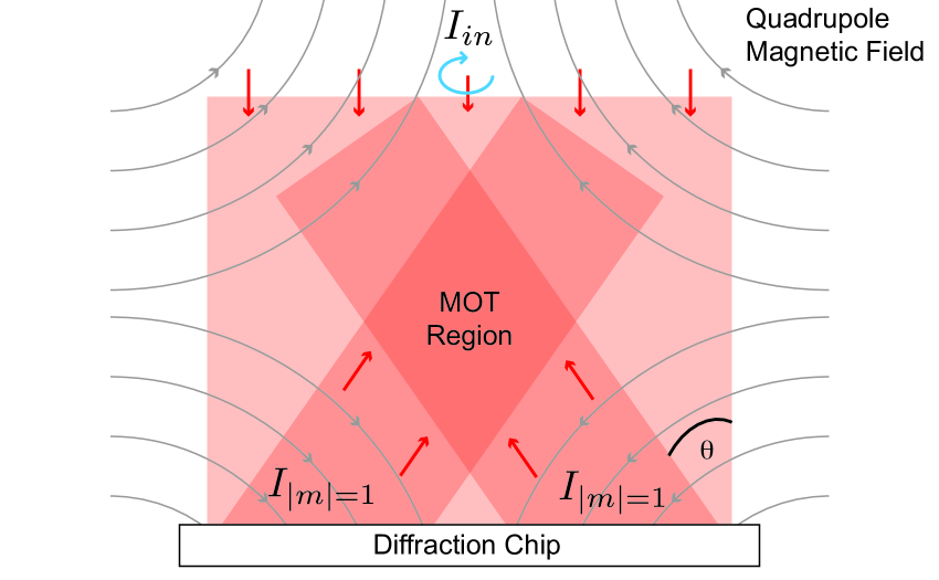
The atoms trapped by the MOT are held by optical scattering forces in the presence of a magnetic quadrupole field. Ideally, these forces should sum to zero at the centre of the quadrupole, which can be achieved by appropriate choices of intensity and polarisation of the light. The chips described here have symmetry that automatically balances the forces parallel to the surface, but balance in the normal direction has to be designed. Let the incident power over an area of the chip produce power in each diffracted beam. The corresponding intensity is , where is the angle to the normal, as shown in Fig. 1. With diffracted beams participating in the MOT, the total intensity contributing to the upward force is . The vertical balance of intensities therefore requires . For chips A and B in Fig. 2, which use three diffracted beams, this condition becomes vangeleyn10 . In practice, the optimum diffracted intensity is somewhat higher because the polarisations of the upward and downward beams are not the same.
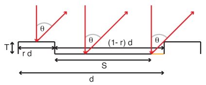
To estimate the power diffracted from our gratings, we approximate them by the ideal profile shown in Fig. 3. The elementary period contains a top face of width and a bottom face of width that is lower by a depth . Light diffracted at an angle from the lower face is shadowed by the step, so that the effective width of the face is . The phase difference between rays coming from the centre of the top surface and the centre of the effective bottom surface is
| (1) |
where and is the wavelength of the light. With a normally incident field , and assuming power reflectivity , the diffracted field at (large) distance is approximated by the Fraunhofer integral.
| (2) |
Here, the first line describes the diffraction from one elementary unit of the grating, as illustrated in Fig. 3, while the last factor sums over the contribution from all grating periods.
The intensity distribution, obtained by squaring equation (2), has a comb of narrow peaks coming from the grating factor, with maxima at the Bragg angles given by , where is an integer. Because many lines of the grating are illuminated, the single-period factor is essentially constant over the small angular spread across one of the Bragg peaks. This makes it straightforward to integrate across the Bragg peak to find the total diffracted power in that order. The result is
being the power incident on the illuminated lines of the grating. Evaluating these integrals,
| (4) | |||||
Let us first consider diffraction into the order - i.e. retro-reflection of the incident beam. This needs to be avoided as a strong upward beam of the wrong polarisation is detrimental to the MOT nshii13 . For chip A there is a plane surface in the central region, which can either be cut away to leave an aperture, or coated with an absorbing layer. For chip B, where the grating structure runs all the way into the middle, the retro-reflection can be suppressed instead by a suitable choice of the grating parameters. On using Eq. (1) to eliminate , Eq. (4) gives
| (5) |
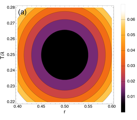
This goes to zero when . Since must be real we require , which leaves . It is desirable to minimise the depth so that remains as large as possible for the first diffraction order. We therefore choose . Fig. 4(a) shows how varies when and deviate from this ideal condition, as they inevitably will in practice. We see that deviations of up to in either or give rise to a of only one or two percent, making the design robust against minor fabrication errors.
We turn now to the first order beams, which (together with the incident beam) are responsible for making the MOT. The plots in Fig. 4(b) (for chip A) and Fig. 4(c) (for chip B) show the power in the order (normalised to ) when the grating depth and duty factor are varied. We see that this power is close to a maximum when the retro-reflected power is zero, but can be increased a little by reducing slightly below 0.5. This has the effect of making and more nearly equal, which improves the contrast of the grating. A little is also gained by reducing , so that the width of the lower surface is increased. As with the minimum of , this maximum of is sufficiently forgiving that we are not troubled by minor fabrication errors.
The MOT works because the scattering force in the presence of a magnetic field depends on the polarisation of the light. For that reason, it would be ideal to go beyond this simple scalar model of the diffraction to consider polarisation. However, that theory is quite challenging and is beyond the scope of this article. Instead we have relied on experiment to determine the polarisation of the diffracted beam, as discussed further in section 4.
3 Fabrication
Chips A and B are produced by two different fabrication methods, which we now describe.
3.1 Chip A: Photo-lithography using silicon substrate
Chip A, shown in Fig. 2a, is a mm square of silicon in which three mm-square lamellar gratings are etched by photolithography. This is then covered with gold to achieve the desired high reflectivity at nm. We choose a grating period of m, which is close to the minimum that can be reliably made by this method. Although we aim for a duty factor of , the bottom face is designed to be nm wide, anticipating that will move towards after the gold is added.
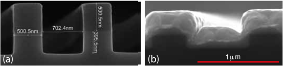
To begin, we make a reticle by direct ebeam writing on chromium-coated quartz. This is a magnified version of one square grating. A -orientated mm-diameter silicon wafer is then coated with SPR photoresist to a thickness of 0.8m and exposed to de-magnified images of the reticle, using light of nm wavelength. A stepper motor manoeuvres the reticle to each grating position in turn, to produce an image of chips - gratings in total - on the wafer. The resist is then developed, and the exposed silicon is removed by reactive ion etching using an inductively-coupled SF6/C4F8 plasma. With a typical etch rate of nm/s, this forms a grating of the desired depth - nm - in under minute. The wafer is then stripped of the remaining resist by plasma ashing, before cleaning with a piranha solution to remove any remaining organic contaminants. Figure 5(a) shows a scanning electron microscope image of a deep grating that was made to calibrate the etch rate. One can see in this image the high quality of the profile and the few-nm accuracy of the widths produced.
In order to give the gratings a high reflectivity, we apply a nm-thick adhesion layer of chromium (by dc sputtering) followed by nm-thick layer of gold (by rf sputtering). The finished grating is shown in Fig. 5b. From this and similar scans we measure a final depth of nm, a period of m and a duty factor of , the latter being due in part to some systematic variation across the chip.
3.2 Chip B: Electron-beam lithography using silicon substrate
Chip B is a mm square of silicon, coated with aluminium, in which a grating is etched by electron beam lithography. The grating consists of nested triangles, as shown magnified in Fig. 2b, that continue outward to fill a mm square. The lamellar surface profile is designed to have a depth of nm, a period of m, and a duty factor of . Unlike the photolithography used for chip A, the e-beam fabrication used here is not at all challenged by the resolution we require. However, the large size of the pattern over all does present a challenge.
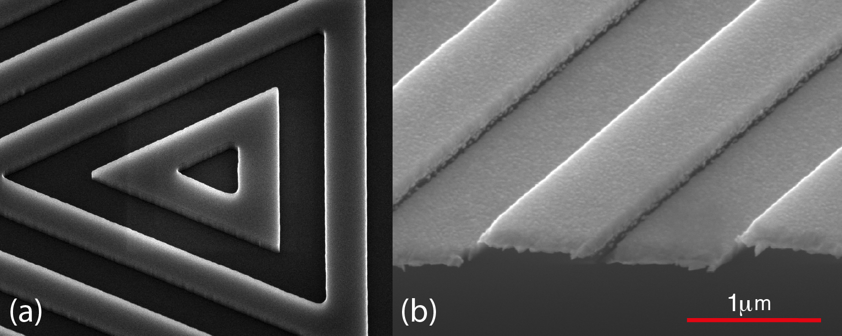
A -orientated mm-diameter silicon wafer is coated with ZEP520A e-beam resist to a thickness of nm, which is then patterned using a high speed e-beam writer (Vistec VB6 with 50MHz scan speed). With chips, covering a total area of , this takes hrs of continuous writing. Particular care is needed to ensure the electron beam direction does not drift over this time, thereby introducing phase variations across individual gratings. The wafer is then etched and cleaned in the same way as chip A. The scanning electron microscope image in Fig. 6(a) shows the centre of the etched grating and illustrates the high quality of the fabrication.
After evaporating nm of aluminium, the grating is imaged again, as shown in Fig. 6(b). From this and similar scans we measure the final parameters T = nm, d = m and r =.
4 Measurement of optical properties
The reflectivity of each chip was determined by measuring the power in a nm laser beam reflected from a flat, un-etched area, and comparing this with the incident power. We found for chip A and for chip B.
In order to measure the diffracted power ratio , a few-milliwatt laser beam of nm wavelength was spatially filtered using a single-mode fibre, then collimated to form a beam of approximately mm full-width-half-maximum. This was sent through a polarising beam splitter, then circularly polarised by a quarter-wave plate, as it would be to make a MOT. Roughly m from the wave plate, the light was retro-reflected from a flat area of the chip and sent back through the wave plate and beam splitter. The circular polarisation of the incident light was optimised by adjusting the angle of the quarter-wave plate to extinguish the light returning through the beam splitter. Next, a translation stage moved the chip so that the light was incident on a grating, and a power meter then recorded the incident power and the power diffracted into first order.
We measured each of the three gratings on chip A, with the results . These are to be compared with the power ratio given by Eq. (4) after inserting the measured grating dimensions and reflectivity. That gives , in good agreement with the measurements. The small variation in both theory and experiment is due predominantly to the variation of . This translates into a variation of the diffracted power because chip A, having , operates on the high-r side of the maximum plotted in Fig. (4)(b), where the derivative with respect to is not zero.
Measurements on the three gratings of chip B gave , showing a good level of reproducibility. This is due in part to better uniformity of the e-beam lithography, but also, chip B operates with , which is very close to the maximum of the plot in Fig. (4)(c), where is insensitive to variation of . The power ratio given by Eq. (4) for chip B is . While this is qualitatively similar to the measured fraction, it does not agree within the measurement uncertainty and we cannot find any plausible adjustment of parameters that might bring them into agreement. We are forced to conclude that our diffraction theory is not able to predict the diffracted power with this high level of accuracy, and suspect that the limitation is due to our use of the effective width , defined by ray optics and therefore not strictly justified. In the case of chip B, the zeroth order beam passes through the MOT, so it is important with this chip to have a low . In order to measure this, we rotated the chip by approximately mrad to separate the diffracted beam from the incident beam. This measurement gave , in good agreement with from Eq. (4).
Because magneto-optical trapping is compromised by the wrong sense of circular polarisation, we looked for this in the first-order diffracted beams using a second combination of quarter-wave plate and polarising beam splitter, adjusted to project the state of the beam onto the basis of left- and right-handed polarisations. Photodetectors at the two beam splitter outputs measured the powers and in each circular polarisation. The fraction of power in the desired polarisation from the three gratings on Chip A was , and , and we note that better polarisation coincided in each case with higher power. On chip B we measured , and . This high degree of polarisation is more than adequate to make a strong MOT with either chip nshii13 . Indeed, although we do not have any calculation for comparison, it seems surprisingly high given the obvious anisotropy of the surface and of the diffraction geometry. We note that the variation in polarisation is greater across chip A than chip B, and again, we ascribe this to the two different methods of fabrication.
5 Summary and conclusions
Optical reflection gratings fabricated on an atom chip offer a simple way to build a large, robust, integrated magneto-optical trap (MOT) for atoms nshii13 . In this paper we have discussed the main design considerations, and have described how suitable chips can be fabricated using two methods: optical lithography and e-beam lithography. Using scalar Fraunhofer diffraction theory and an idealised model of the lamellar profile, we have provided an account of the expected MOT beam intensities. This theory agrees well with experiment down to the level of a few percent of the incident power, but not with the higher-precision measurements made on the aluminium-coated chip B. We have shown that it is possible to suppress the back-reflection, while at the same time diffracting a large fraction of the power into the two first-order beams. The power in these beams depends on the choice of period , duty factor and depth of the grating. These parameters vary a little over the optically fabricated chip A, and rather less over the e-beam fabricated chip B. In either case, we show how to minimise the effect of inhomogeneity on the diffracted beam intensity by operating at the intensity maximum with respect to and . We also find that the circular polarisation of the light is surprisingly well preserved after diffraction into the first-order beams.
The design principles and theoretical model developed here make this new method accessible to anyone who may wish to incorporate such an integrated trap into an atom chip. We anticipate that this approach will facilitate future quantum technologies using cold and ultra-cold atoms rushton14 .
Acknowledgments
The authors acknowledge valuable conversations with Alastair Sinclair of the National Physical Laboratory. This work was supported by the UK EPSRC, ESA (through ESTEC project TEC- MME/2009/66), the CEC FP7 (through project 247687; AQUTE). JPC was funded by an EPSRC support fund and VCQ fellowship, P.G. by the Royal Society of Edinburgh and E.H. by the Royal Society.
References
- [1] C. C. Nshii, M. Vangeleyn, J. P. Cotter, P. F. Griffin, E. A. Hinds, C. N. Ironside, P. See, A. G. Sinclair, E. Riis, and A. S. Arnold. A surface-patterned chip as a strong source of ultracold atoms for quantum technologies. nature nanotechnology, 8:321 – 324, 2013.
- [2] J. P. McGilligan, P. F. Griffin, E. Riis, and A. S. Arnold. Phase-space properties of magneto-optical traps utilising micro-fabricated gratings. Opt. Express, 23(7):8948–8959, Apr 2015.
- [3] G. N. Lewis, Z. Moktadir, C. Gollasch, M. Kraft, S. Pollock, F. Ramirez-Martinez, J. Ashmore, A. Laliotis, M. Trupke, and E. A. Hinds. Fabrication of magnetooptical atom traps on a chip. J. MEMS, 18:347 – 353, 2009.
- [4] S. Pollock, J. P. Cotter, A. Laliotis, and E. A. Hinds. Integrated magneto-optical traps on a chip using silicon pyramid structures. Optics Express, 17:14109 – 14114, 2009.
- [5] S. Pollock, J. P. Cotter, A. Laliotis, F. Ramirez-Martinez, and E. A. Hinds. Characteristics of integrated magneto-optcal traps for atom chips. New J. Phys., 13:043029, 2011.
- [6] E. A. Hinds and I. G. Hughes. Magnetic atom optics: mirrors, guides, traps, and chips for atoms. Journal of Physics D: Applied Physics, 32(18):R119, 1999.
- [7] N. H. Dekker, C. S. Lee, V. Lorent, J. H. Thywissen, S. P. Smith, M. Drndić, R. M. Westervelt, and M. Prentiss. Guiding neutral atoms on a chip. Phys. Rev. Letts., 84:1124, 2000.
- [8] S. Eriksson, M. Trupke, H. F. Powell, D. Sahagun, C. D. J. Sinclair, E. A. Curtis, B. E. Sauer, E. A. Hinds, Z. Moktadir, C. O. Gollasch, and M. Kraft. Integrated optical components on atom chips. Eur. Phys. J. D, 35:135 – 139, 2005.
- [9] P. Treutlein, P. Hommelhoff, T. Steinmetz, T. W. Hänsch, and J. Reichel. Coherence in microchip traps. Phys. Rev. Letts., 92:203005, 2004.
- [10] W. Hänsel, P. Hommelhoff, T. W. Hänsch, and J. Reichel. Bose-Einstein condensation on a microelectronic chips. Nature, 413:498–501, 2001.
- [11] H. Ott, J. Fortágh, F. Schlotterback, A. Grossmann, and C. Zimmermann. Bose-Einstein condensation in a surface microtraps. Phys. Rev. Letts., 23:230401, 2001.
- [12] T. Schumm, S. Hofferberth, L. M. Andersson, S. Wildermuth, S. Groth, I. Bar-Joseph, J. Schmiedmayer, and P. Krüger. Matter-wave interferometry in a double well on an atom chip. Nat. Phys., 1:57–62, 2005.
- [13] F. Baumgärtner, R. J. Sewell, S. Eriksson, I. Llorente-Garcia, J. Dingjan, J. P. Cotter, and E. A. Hinds. Measuring energy differences by BEC interferometry on a chips. Phys. Rev. Letts., 105:243003, 2010.
- [14] M. F. Riedel, P. Böhi, Y. Li, T. W Hänsch, A. Sinatra, and P. Treutlein. Atom-chip-based generation of entanglement for quantum metrology. Nature, 464:1170, 2010.
- [15] K. Lindquist, M. Stephens, and C. Wieman. Experimental and theoretical-study of the vapor-cell zeeman optical trap. Phys. Rev. A, 46(7):4082–4090, 1992.
- [16] J. Reichel, W. Hänsel, and T. W. Hänsch. Atomic micromanipulation with magnetic surface traps. Phys. Rev. Lett., 83:3398–3401, Oct 1999.
- [17] K. I. Lee, J. A. Kim, H. R. Noh, and W. Jhe. Single-beam atom trap in a pyramidal and conical hollow mirror. Opt. Letts., 21:1177, 1996.
- [18] A. Laliotis, M. Trupke, J. P. Cotter, G. Lewis, M. Kraft, and E. A. Hinds. ICP polishing of silicon for high-quality optical resonators on a chip. Journal of Micromechanics and Microengineering, 22(12):125011, 2012.
- [19] J P Cotter, I Zeimpekis, M Kraft, and E A Hinds. Improved surface quality of anisotropically etched silicon planes for mm-scale optics. Journal of Micromechanics and Microengineering, 23(11):117006, 2013.
- [20] M. Vangeleyn, P.F. Griffin, E.Riis, and A. S. Arnold. Single-laser, one beam, tetrahedral magneto-optical trap. Opt. Express, 17(16):13601–13608, 2009.
- [21] M. Vangeleyn, P. F. Griffin, E. Riis, and A. S. Arnold. Laser cooling with a single laser beam and a planar diffractor. Opt. Lett., 35(20):3453–3455, Oct 2010.
- [22] J. A. Rushton, M. Aldous, and M. D. Himsworth. Contributed review: The feasibility of a fully miniaturized magneto-optical trap for portable ultracold quantum technology. Review of Scientific Instruments, 85(12), 2014.