Quantum confinement : A route to enhance the Curie temperature of Mn doped GaAs
Abstract
The electronic structure of Mn doped GaAs and GaN have been examined within a multiband Hubbard model. By virtue of the positioning of the Mn states, Mn doped GaAs is found to belong to the - metal regime of the Zaanen-Sawatzky-Allen phase diagram and its variants while Mn doping in GaN belongs to the covalent insulator regime. Their location in the phase diagram also determines how they would behave under quantum confinement which would increase the charge transfer energy. The ferromagnetic stability of Mn doped GaAs, we find, increases with confinement therefore providing a route to higher ferromagnetic transition temperatures.
While early research on dilute magnetic semiconductors focussed on II-VI semiconductorsFurdyna-1988 ; Corbett-1983 , the possibility of using low temperature molecular beam epitaxy for the growth shifted the focus onto III-V semiconductorsOhno-1996 ; samarth-2002 ; nature-2005 ; rmp-2014 ; freeland-2003 . Additionally the growth technique allowed the introduction of transition metal atoms far beyond their equilibrium solubility. The quest for higher concentrations of the transition metal in the semiconductor was driven by considerations of increasing the magnetic ordering temperature. However initially various material issues plagued the discovery of new dilute magnetic semiconductors and one was never sure if the magnetism was intrinsic or due to impurity phases. With recent developments in both the growth as well as the characterization of dilute magnetic semiconductors, puzzling observations are emerging which don’t seem to be explainable within the current models used to explain magnetism. Considering the well studied example of GaAs doped with Mn, which is believed to represent a system where the magnetism is intrinsic, the highest Curie temperature has been found to be around 185 KNovak-2008 . However, recent photoemission experiments found spin polarized bands even at room temperaturearxiv-2014 and this can’t be reconciled with the existing models for ferromagnetism.
Further the same transition metal atom doped in different semiconductors has led to varying behavior APL-2001 ; gamnn . This was initially explained within the kinetic exchange model in which each transition metal atom was approximated by a spin. This spin interacted with the valence band of the host semiconductor, resulting in a spin polarization of the carriers which mediated the magnetism Dietl-1997 . Later models questioned this hypothesis and put forth the picture of an impurity band emerging from the interaction of the transition metal with the host semiconductorMahadevan-2004 ; APL ; RKKY . However this description has remained at a qualitative levelAPL ; RKKY . The picture of the impurity band emerging in GaAs doped with Mn has been supported by recent experiments tanaka ; dobrowolska ; fujii . There have also been improved approaches to examine the electronic structurefujii ; dmft , however, there is still no consensus on the mechanism of magnetism.
Bulk transition metal compounds have been studied for a long time and their electronic structure is well established within the framework of the Zaanen-Sawatzky-Allen (ZSA) phase diagramZSA-1985 ; Nimkar-1993 ; DD-pramana . A similar framework should be possible for dilute magnetic semiconductors which we examine in the present work. We consider a multiband Hubbard model to describe the electronic structure of the dilute magnetic semiconductor with Coulomb interactions included on the transition metal site. Parameters appropriate for Mn doped GaAs place it in the regime of a - metal of the ZSA phase diagram, thereby explaining why correlation effects don’t drive it insulating. Quantum confinement effects can be used to tune the charge transfer energy , driving a change in the character of the hole state. We show that this also serves as a parameter to change the Curie temperature, with the largest ferromagnetic stability being in the vicinity of equal to zero. is the charge transfer energy defined between the Mn states and the dangling bond states with symmetry. Confinement arising from the presence of the surface could lead to the same effect of enhancing the Curie temperature, therefore explaining the experimental observation of spin polarized bands even at room temperaturearxiv-2014 . Mn doped GaN is found to be a covalent insulator within the framework of our calculations, thereby explaining the different behavior found for Mn doping in GaAs and GaN.
In order to discuss various aspects of the electronic structure of Mn doped GaAs, a multiband Hubbard model is set up to solve the electronic structure. In this model, states are included on the Mn atom, , states are included on the Ga atoms while ,, states are included on the As atoms. Hopping is allowed between nearest neighbor Mn and As atoms, between Ga and As atoms as well as between nearest neighbor Ga-Ga and As-As atoms. The onsite energies as well as the hopping interaction strengths are determined by fitting the ab-initio band structure suppl-info of nonmagnetic 25% Mn doped GaAs calculated within VASPJoubert ; vasp ; vasp1 to a tight-binding modelPRB-TB . Onsite Coulomb interactions between the orbitals on Mn are parametrised in terms of the Slater-Condon integrals , and . While and are fixed at 80 of their atomic Hartree-Fock values, is fixed so that the multiplet averaged is at a pre-determined value. In the rest of the discussion, we use only the multiplet averaged . A similar tight binding fitting of the ab-initio band structure for nonmagnetic 25 Mn doped GaN is carried out to determine the one electron part of the multiband Hubbard Hamiltonian for Mn doped GaN which is then solved. A mean field decoupling scheme has been used for the four fermion terms in the Hamiltonian which is solved self-consistently for the order parameters as discussed earlierLa2NiO4-1997 ; Nimkar-1993 over a 4x4x4 k-points grid for the 64 atoms supercell. In order to explore magnetism, a spin spiral implementation is considered which uses the generalised Bloch’s theorem so that the same unit cell could be used for different magnetic configurations characterised by the wave vector eschrig-1998 .
Early work on transition metal compounds established the important role that correlations played in driving the system insulatingminami . As the nature of the ground state was largely determined by electron-electron interactions at the transition metal site, it was a surprise when it was found that on changing the anion in a set of late 3 transition metal compounds, one had large changes in the bandgaps, with even metallic members being foundminami . This established that in addition to the onsite Coulomb interactions (), there was another scale in the problem, which was the cost of charge transfer () between the anion states and the transition metal states. This was brought out by Zaanen, Sawatzky and AllenZSA-1985 in their seminal phase diagram which now forms the basis for classifying the electronic structure of transition metal compounds. We now consider examples of two well-studied semiconductors - GaAs:Mn and GaN:Mn and examine in which regime they lie in the ZSA phase diagram.
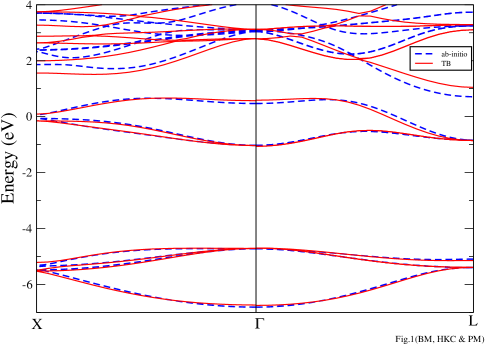
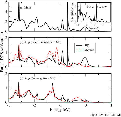
The band dispersions for nonmagnetic 25 Mn doped GaAs are given in Fig. 1. The ab-initio band dispersions are given by the dashed blue lines, while the best tight-binding fit are given by the solid red lines. The fitting procedure involves an optimization of the best fit band structure along various symmetry directions by a least square error minimization processPRB-TB . The bare charge transfer energy between the Mn states and the As states estimated from the fitting is found to be 0.53 eV. Other parameters extracted from the fitting are given in the Supplementary Information. We then use these parameters as the tight binding part of a multiband Hubbard Hamiltonian and calculate the electronic structure of Mn doped GaAs at a doping percentage of 3.125 which is within the range of concentrations probed in experiments. The calculated partial density of states is shown in Fig. 2 where the zero of the energy scale is the Fermi energy. One finds that the up spin states with dominantly Mn character lie deep inside the valence band with some weight at the Fermi energy also. The As atoms which are the nearest neighbors of the Mn atom are found to contribute primarily to the state at the Fermi level while those atoms which are far away have a weak contribution. The spin polarization of the states localized on the nearest neighbors of the Mn atom is large while it is weaker for the states associated with the farther away As atoms. This is consistent with the impurity model descriptionMahadevan-2004 ; RKKY ; APL introduced by Mahadevan and Zunger in which the electronic structure of Mn doped GaAs can be visualised as arising from the interaction of the levels on Mn with the states present prior to the introduction of the Mn atom at a Ga site (i.e the dangling bond states associated with a Ga-vacancy). The interaction is primarily between the levels with symmetry on Mn and the levels with the same symmetry on the dangling bonds. These dangling bond states are dominantly localized on the As atoms which are the nearest neighbors of the Mn atom. Consequently one finds that the states at the Fermi energy which are the antibonding states of these interactions are localized on these atoms. A of 3 eV is used on Mn, though we have also increased the value from 3 eV to 4 eV to examine its effect on the electronic structure. The calculated Mn partial density of states for =4 eV is shown in the inset of Fig. 2(a) and the system is still metallic. Hence considering reasonable values of U on Mn does not drive Mn doped GaAs insulating.
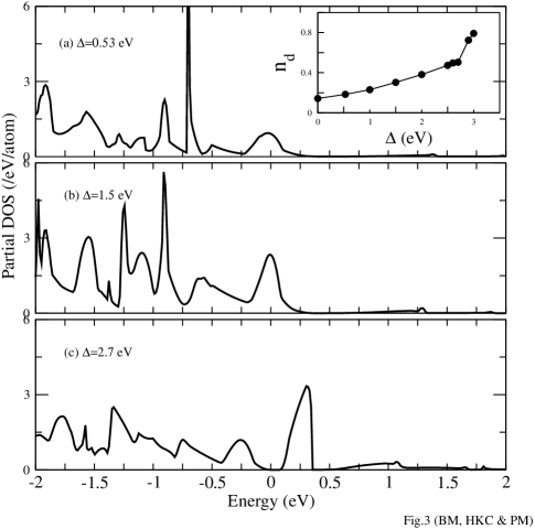
The definition of should be with respect to the energy of the dangling bond states with symmetry and is referred to as in the subsequent discussion. As this is difficult to determine precisely, we vary and examine the character of the hole state. When the two interacting levels are degenerate (=0) one expects that the hole has equal weight on Mn as well as the interacting As atoms. In Fig. 3 we have plotted the variation of the Mn partial density of states as a function of . As is increased, one finds an increase in the Mn contribution to the hole state. Tracking the Mn character of this state () (inset of Fig. 3), one finds that between of 2.6 and 2.7 eV one has a change over with the hole becoming predominantly Mn like. This places =0 near a of 2.7 eV in contrast to the value of 0.53 eV found from the fitting. Hence Mn doped GaAs is in the negative regime of the ZSA phase diagram. As it is metallic, we identify it as a - metal. While the charge transfer energy is usually a fixed quantity for a system, here, is referenced with respect to the dangling bond states. The dangling bond states follow the valence band maximum of the host semiconductor. The latter can be tuned in a semiconductor by quantum confinementQ-confinement . The state corresponding to the bulk case (=0.53 eV) may be described by the configuration where locally Mn is found to be , and so is Mn2+-like. In the regime where 0, Mn may be represented by the configuration and is therefore in the valence state Mn3+. Hence one has a valence transition with decrease in size of Mn doped GaAs. The valence transition has been discussed earlier in the literature by Sapra et al.sapra-2002 using a tight binding model. What we show is that a metal-insulator transition accompanies this valence transition.
The immediate question which follows is how does the stability of the ferromagnetic state change with quantum confinement. We examine this by considering an isolated Mn impurity in the 64 atom unit cell (i.e, a doping percentage of 3.125 ) and comparing the energies of the ferromagnetic as well as the totally antiferromagnetic configuration given by =0.5 0.5 0.5. The Mn atoms are separated by 11.3 . The interaction between them is weak and so for small values, one finds that the different magnetic solutions have comparable energies (Table I). For larger values we have the system favoring an antiferromagnetic ground state. This is in contrast with experiments which find ferromagnetismAPL-2001 . However Mn atoms show a tendency to clusterAPL-cluster ; raebiger3 and the high magnetic ordering temperatures observed have been associated with the presence of these clustersakash ; APL-2004 ; APL-2006 . We therefore went on to examine the variations in the ferromagnetic stability by considering pairs of Mn atoms occupying FCC nearest neighbor positions as well as fourth neighbor positions where the separations are 3.995 Å and 7.99 Å respectively. The difference in energy between the ferromagnetic as well as antiferromagnetic configuration are given in Table II. As is increased, one finds that the ferromagnetic stability increases till a of 2.3 eV for pairs of Mn atoms at first neighbor positions and then it begins to decrease. This can be traced to the fact that for a of 2.7 eV we had the Mn and dangling bond states almost degenerate for 1 Mn. The presence of the second Mn at the nearest neighbor position changes some details of the at which the two interacting levels are degenerate. The result is that the ferromagnetism is stabilized by superexchange between the Mn atoms involving the intervening As atom, explaining the enhanced ferromagnetic stability at =0. The calculated ferromagnetic stability at fourth neighbor also shows a similar trend, being largest at =2.6 eV.
Mn doping in bulk GaAs has a ferromagnetic stability of 73 meV for nearest neighbor atoms. The increase till 0 is approached reflects the fact that with quantum confinement one can achieve transition temperatures higher than what is encountered in bulk GaAs. This may be able to explain the experimental observation of spin polarized bands at room temperature found in recent spin resolved photoemission experimentsarxiv-2014 .
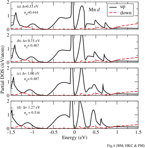
A similar analysis was carried out for Mn doped GaN to determine the tight binding parameters as well as onsite energies. The extracted parameters suppl-info gave us a of 1.27 eV for Mn doping in bulk GaN and the hole has 0.516 Mn character () (Fig. 4). A small decrease of to 1.0 eV reduces the to 0.487. This places 0 at 1.15 eV. Our analysis ignored the width of the Mn states and the N states and defined with respect to the centroid of the Mn band. Taking this into account we can place Mn doped GaN in the regime where is negative. It is then surprising that we have an insulating ground state. This phase has been called the covalent insulator and has been shown to exist in the ZSA phase diagram by Sarma and co-workersNimkar-1993 ; DD-pramana . Strong covalency between the transition metal and the anion are responsible for the insulating state. It is evident from its location in the phase diagram that any increase in arising from quantum confinement effects would not be useful in tuning the magnetic transition temperature in Mn doped GaN.
The electronic structure of Mn doped GaAs and GaN have been examined within a multiband Hubbard model. The former may be placed in the - metal regime of the ZSA phase diagram or its variants while the latter belongs to the covalent insulating regime. Quantum confinement allows us to tune the effective charge transfer energy and its effect on the ferromagnetic ordering temperature depends on where they lie within the ZSA phase diagram. This then provides us with a route to higher ordering temperatures in the dilute magnetic semiconductors.
BM acknowledges CSIR, India for financial support. HKC and PM thanks the Department of Science and Technology, India.
References
- (1) Semiconductors and Semimetals, Vol. 25, edited by J. K. Furdyna and J. Kossut, (Academic Pres, New York, 1988); C. Delerue, M. Lannoo and G. Allan, Phys. Rev. B 39, 1669 (1989).
- (2) J. Schneider, Defects in Semiconductors II, Symposium Proceedings, edited by S. Mahajan and J. W. Corbett, (North Holland, Amsterdam 1983), p.225; B. Clerjaud, J. Phys. C 18, 3615 (1985).
- (3) H. Ohno, A.Shen, F. Matsukura, A.Oiwa, A. Endo, S. Katsumoto and Y. Iye, Appl. Phys. Lett. 69, 363 (1996).
- (4) S. J. Potashnik, K. C. Ku, R. Mahendiram, S. H. Chun, R. F. Wang, N. Samarth and P. Schiffer, Phys. Rev. B 66, 012408 (2002).
- (5) A. H. MacDonald, P. Schiffer and N. Samarth, Nat. Mater. 4, 195 (2005).
- (6) T. Dietl and H. Ohno, Rev. Mod. Phys. 86, 187 (2014).
- (7) D. J. Keaney, D. Wu, J. W. Freeland, E. Johnston-Halperin, D. D. Awschalom and J. Shi, Phys. Rev. Lett. 91, 187203 (2003).
- (8) V. Novák, K. Olejník, J. Wunderlich, M. Cukr, K. Výborný, A.W. Rushforth, K.W. Edmonds, R.P. Campion, B.L. Gallagher, Jairo Sinova, and T. Jungwirth, Phys Rev Lett 101, 077201 (2008).
- (9) J. Kanski, L. Ilver, K. Karlsson, M. Leandersson, I. Ulfat and J. Sadowski, arXiv:1410.8842 (2014).
- (10) S. J. Potashnik, K. C. Ku, S. H. Shun, J. J. Berry, N. Samarth and P. Shiffer, Appl. Phys. Lett. 79, 1495 (2001).
- (11) E. Sarigiannidou, F. Wilhelm, E. Monroy, R. M. Galera, E. Bellet-Amalric, A. Rogalev, J. Goulon, J. Cibert, and H. Mariette, Phys. Rev. B 74, 041306 (2006).
- (12) T. Dietl, H. Ohno, F. Matsukura, J. Cibert and D. Ferrand, Science 287, 1019 (2000).
- (13) P. Mahadevan, A. Zunger and D. D. Sarma, Phys. Rev. Lett. 93, 177201 (2004).
- (14) P. Mahadevan and A. Zunger, Appl. Phys. Lett. 85, 2860 (2004).
- (15) P. Mahadevan and A. Zunger, Phys. Rev. B 69, 115211 (2004).
- (16) Shinobu Ohya, Iriya Muneta, Pham Nam Hai and Masaaki Tanaka, Phys. Rev. Lett 104, 167204 (2010).
- (17) M. Dobrowolska, K. Tivakornsasithorn, X. Liu, J.K. Furdyna, M. Berciu, K.M. Yu and W. Walukiewicz, Nat. Mater. 11, 444 (2012).
- (18) J. Fujii, B.R. Salles, M. Sperl, S. Ueda, M. Kobata, K. Kobayashi, Y. Yamashita, P. Torelli, M. Utz, C. S. Fadley, A.X. Gray, J. Braun, H. Ebert, I. Di Marco, O. Eriksson, P. Thunstrm, G. H. Fecher, H. Stryhanyuk, E. Ikenaga, J. Minar, C.H. Back, G. ven der Laan and G. Panaccione, Phys. Rev. Lett. 111, 097201 (2013).
- (19) I. Di Marco, P. Thunström, M.I. Katsnelson, J. Sadowski, K. Karlsson, S. Lebègue, J. Kanski and O. Eriksson, Nat. Comm. 4, 2645 (2013).
- (20) J. Zaanen, G. A. Sawatzky and J. W. Allen, Phys. Rev. Lett. 55, 418 (1985).
- (21) S. Nimkar, D. D. Sarma, H. R. Krishnamurthy and S. Ramasesha, Phys. Rev. B 48, 7355 (1993).
- (22) D. D. Sarma, H. R. Krishnamurthy, S. Nimkar, S. Ramasesha, P. P. Mitra and T. V. Ramakrishnan, Pramana 38, 531 (1992).
- (23) G. Kresse and D. Joubert, Phys. Rev. B 59, 1758 (1999).
- (24) G. Kresse, and J. Furthmller, Phys. Rev. B 54, 11169 (1996).
- (25) G. Kresse, and J. Furthmller, Comput. Mat. Sci. 6, 15 (1996).
- (26) See Supplementary Information for more details.
- (27) P. Mahadevan, N. Shanthi and D. D. Sarma, Phys. Rev. B 54, 11199 (1996).
- (28) P. Mahadevan, K. Sheshadri, D. D. Sarma, H.R. Krishnamurthy and Rahul Pandit, Phys. Rev. B 55, 9203 (1997).
- (29) S. V. Halilov, H. Eschrig, A. Y. Perlov and P. M. Oppeneer, Phys. Rev. B 58, 293 (1998).
- (30) A. Fujimori and F. Minami, Phys. Rev. B 30, 951 (1984).
- (31) S. Sapra, D. D. Sarma, S. Sanvito and N. A. Hill, Nano Lett. 2, 605 (2002).
- (32) R. Viswanatha, S. Sapra, T. Saha-Dasgupta and D. D. Sarma, Phys. Rev. B 72, 045333 (2005).
- (33) P. Mahadevan, J. M. Osorio-Guillen and A. Zunger, Appl. Phys. Lett. 86, 172504 (2005).
- (34) M. van Schilfgaarde and O. N. Mryasov, Phys. Rev. B 63, 233205 (2001).
- (35) I. Ulfat, J. Kanski, L. Ilver, J. Sadowski, K. Karlsson, A. Ernst and L. Sandratskii, Phys. Rev. B 89, 045312 (2014).
- (36) A. Chakraborty, R. Bouzerar, S. Kettemann and G. Bouzerar, Phys. Rev. B 85, 01420 (2012).
- (37) G. Bouzerar, T. Ziman and J. Kudmovsky, Appl. Phys. Lett. 85, 4941 (2004).
- (38) T. Hynninen, H. Raebiger, J. von Boehm and A. Ayuela , Appl. Phys. Lett. 88, 122501 (2006).
| (in eV) | E[q=(0.5 0.5 0.5)]-E[(q=0 0 0)] (in eV) |
| 0.53 | -0.002 |
| 1.00 | -0.005 |
| 1.50 | -0.007 |
| 2.00 | -0.009 |
| 2.50 | -0.011 |
| 2.60 | -0.011 |
| 2.80 | -0.044 |
| 2.90 | -0.049 |
| 3.00 | -0.070 |
| 1st nearest neighbor | 4th nearest neighbor | |
|---|---|---|
| (in eV) | E(AFM-FM) in eV | E(AFM-FM) (in eV) |
| 1.5 | 0.120 | 0.048 |
| 1.7 | 0.133 | 0.056 |
| 1.8 | 0.140 | 0.057 |
| 1.9 | 0.147 | 0.059 |
| 2.1 | 0.161 | 0.067 |
| 2.2 | 0.167 | 0.069 |
| 2.3 | 0.174 | 0.072 |
| 2.4 | 0.146 | 0.080 |
| 2.5 | 0.116 | 0.083 |
| 2.6 | 0.065 | 0.099 |
| 2.9 | 0.011 | 0.074 |