∎
Josephson coupling in junctions made of monolayer graphene grown on SiC
Abstract
Chemical vapor deposition has proved to be successful in producing graphene samples on silicon carbide (SiC) homogeneous at the centimeter scale in terms of Hall conductance quantization. Here we report on the realization of co-planar diffusive Al/ monolayer graphene/ Al junctions on the same graphene sheet, with separations between the electrodes down to 200 nm. Robust Josephson coupling, as the magnetic pattern of the critical current, has been measured for separations not larger than 300 nm. Transport properties are reproducible on different junctions and indicate that graphene on SiC substrates is a concrete candidate to provide scalability of hybrid Josephson graphene/superconductor devices.
Keywords:
Graphene, Josephson effect, Silicon Carbide1 Introduction
The remarkable electrical properties of graphene, induced by the chiral nature of its charge carriers, rises big expectations presently, of increasing functionalities in hybrid superconducting quantum devices. Josephson junctions in which the supercurrent flows through normal-conducting graphene across closely spaced Superconductors (S), have been realized up to now only with exfoliated graphene. Usually the graphene flakes are deposited on a Si/SiO2 substrate[1, 2, 3, 4, 5, 6, 7, 8].
Even if the achievements are for many respects spectacular at present, the goal of realizing whatever simple hybrid circuit with a number of these junctions on the same graphene sheet is a long way off, because of the severe limits imposed by the present fabrication protocols. Every junction will have its own properties (and story), with no chance of controlling the electrodynamics and its functionality, when engineering the full circuit.
In this work we propose to use Chemical Vapor Deposition (CVD) of graphene on large silicon carbide (SiC) areas, which does not require subsequent exfoliation. We report on the characteristics of the fabricated junctions, demonstrating that the high quality of the devices, patterned on a single graphene sheet, paves the way to finally taking on this limit, an utmost priority in view of any future application.
Graphene made by CVD on metals[9] and graphene on SiC cover large surfaces and are homogeneous at the centimetre scale. Thus relatively simple lithography processes allow to obtain thousands of devices on the same wafer[10]. The mobility of graphene grown by CVD on metals is mainly limited by defects introduced during the transfer process[11], whereas the mobility of graphene on SiC is essentially controlled by the carrier concentration. In graphene on SiC, the mobility can reach cm2V-1s-1 at =2 K and at carrier concentrations cm-2[12]. This corresponds to a mean free path 80 nm. Additionally, the quantum Hall effect of graphene on SiC is remarkably precise even at magnetic fields as low as T[13, 14], which makes graphene on SiC the material of choice for the next generation of easy-to-use quantum electrical standards. By combining Josephson arrays supporting relatively large magnetic fields and Hall bars made of graphene, complex metrological devices like quantum current standards could be designed on the same wafer[15, 16]. Besides, the interface and/or the surface of graphene on SiC can be modified. Various atomic species like oxygen, hydrogen, calcium, can be intercalated or deposited whereas it is well established that intercalated graphite or few layer graphene become superconductive[17, 18, 19]. Thus, CVD graphene on SiC is also a good platform to study graphene-based superconductivity[20].
2 Sample Characterization and preparation
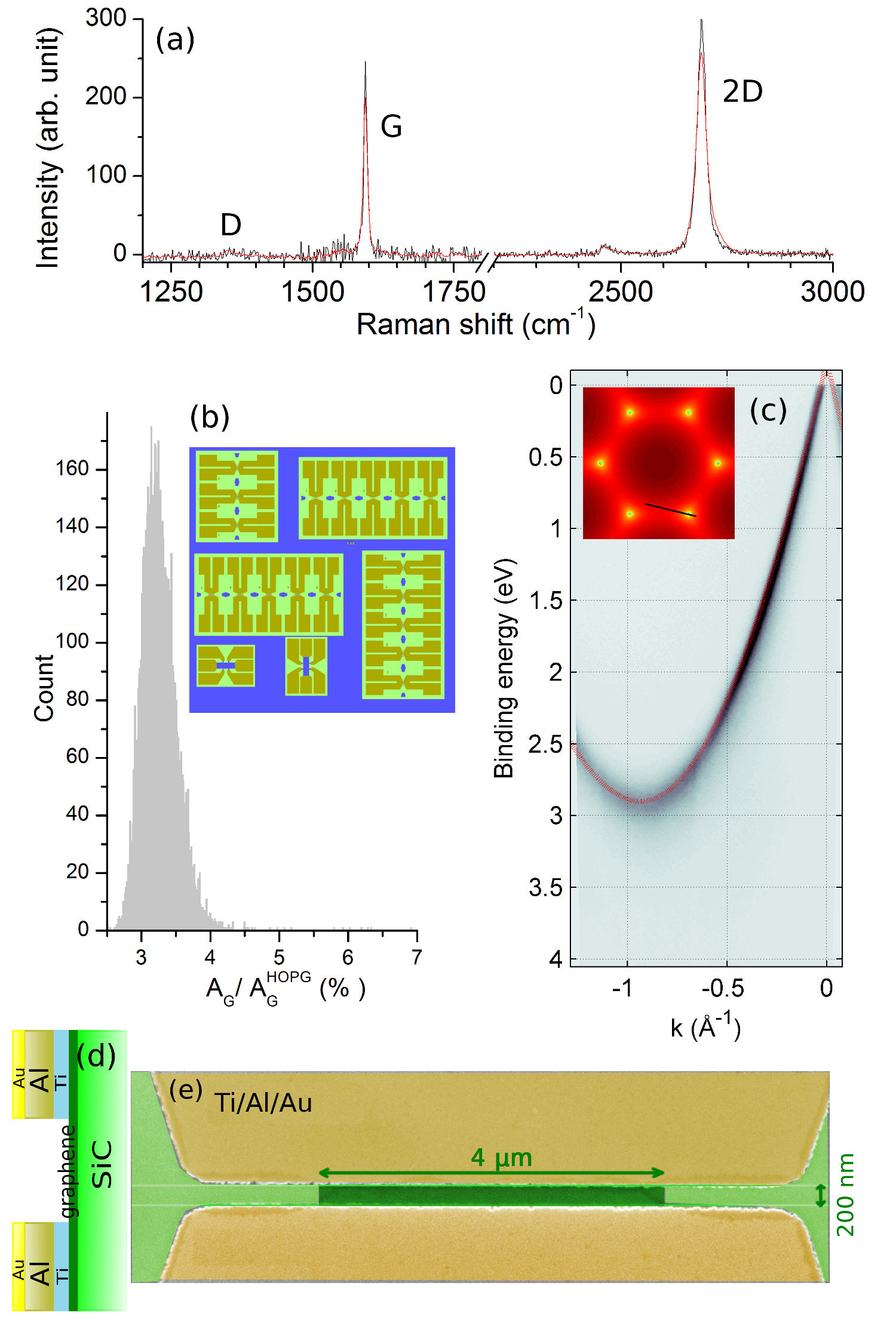
Graphene has been grown by propane-hydrogen CVD[23] on the Si face of a semi-insulating -off-axis 6H-SiC substrate purchased from TankeBlue, using conditions similar to those used in Ref. [24]. The growth is done in one minute, at a temperature of 1550 ∘C under a 800 mbar atmosphere made of argon, propane and hydrogen (3 slm argon, 10 slm hydrogen, 5 sccm propane). The substrate is then cleaved to obtain several samples of total size mm mm. Fig. 1 resumes the structural characteristics of the graphene samples. Raman spectra, obtained after the growth, are reported in panel (a). For 98% of the surface, the integrated intensity of the peak, normalized with respect to a graphite reference, is about %, see panel (b). This is very close to the experimental value reported for a graphene monolayer[21]. By contrast, bilayer graphene would yield about twice this intensity[21]. ARPES measurements, carried out on the Cassiopée beamline at the synchrotron radiation facility SOLEIL, reveals that the sample is a -doped monolayer graphene, see panel(c). On a similar growth, magnetotransport measurements also revealed the half-integer quantum Hall effect specific to monolayer graphene[24]. The ARPES measurements are done under ultra-high vacuum, after an initial degassing performed at 500 oC. On the silicon-face of SiC, the graphene is usually -doped, because of the presence of the so-called carbon-rich interface. Here, the -doping is the experimental signature that this carbon-rich interface has been neutralized and replaced by an hydrogenated interface between graphene and SiC[24].
Van der Pauw and Hall measurements, done before lithography on the mm mm sample, give a carrier concentration cm-2 and a mobility cmVs-1 at room temperature under ambient atmosphere. This corresponds to a sheet resistivity , with a form factor which evidences a small anisotropy of conductivity linked to the SiC steps. The low mobility is typical for graphene on SiC which is not compensated. In principle, mobility higher by one order of magnitude can be obtained by an appropriate gating which would reduce the carrier concentration[12]. As both ARPES and Hall measurements give similar carrier concentration, the atmospheric contamination plays a minor role and is not the main source of doping, which is likely to be due to the interface.
The Josephson devices are fabricated by conventional e-beam lithography. The graphene junctions are patterned by oxygen plasma. Then, the contacts are deposited, see Fig. 1(d,e). They consist of a 5 nm interfacial layer of titanium, a 80 nm thick aluminium layer and a 3 nm thick gold layer. The gaps between the electrodes ranges from 200 nm to 600 nm. The width is fixed at m. A total of twelve junctions have been defined, with two orientations with respect to the substrate. The samples have been thermally anchored to the 3He pot of a 3He cryostat (Heliox VL Oxford Instruments) and four probes electrical measurements have been performed. The cryostat is equipped with a room temperature electromagnetic interference filter stage followed by low pass RC filters anchored at 1.5 K and by copper powder filters stage anchored at the sample stage[25]. Standard measurements of current-voltage characteristics as a function of temperature and magnetic field along with curves with a bias current of about 5 nA have been performed. In addition, conductance spectra have been measured by superimposing a low amplitude (a few nA) sinusoidal signal with frequency of about 30 Hz to a triangular slow ramp, with a frequency of about 1 mHz, and by reading the response from the sample by using the lock-in technique.
3 Results
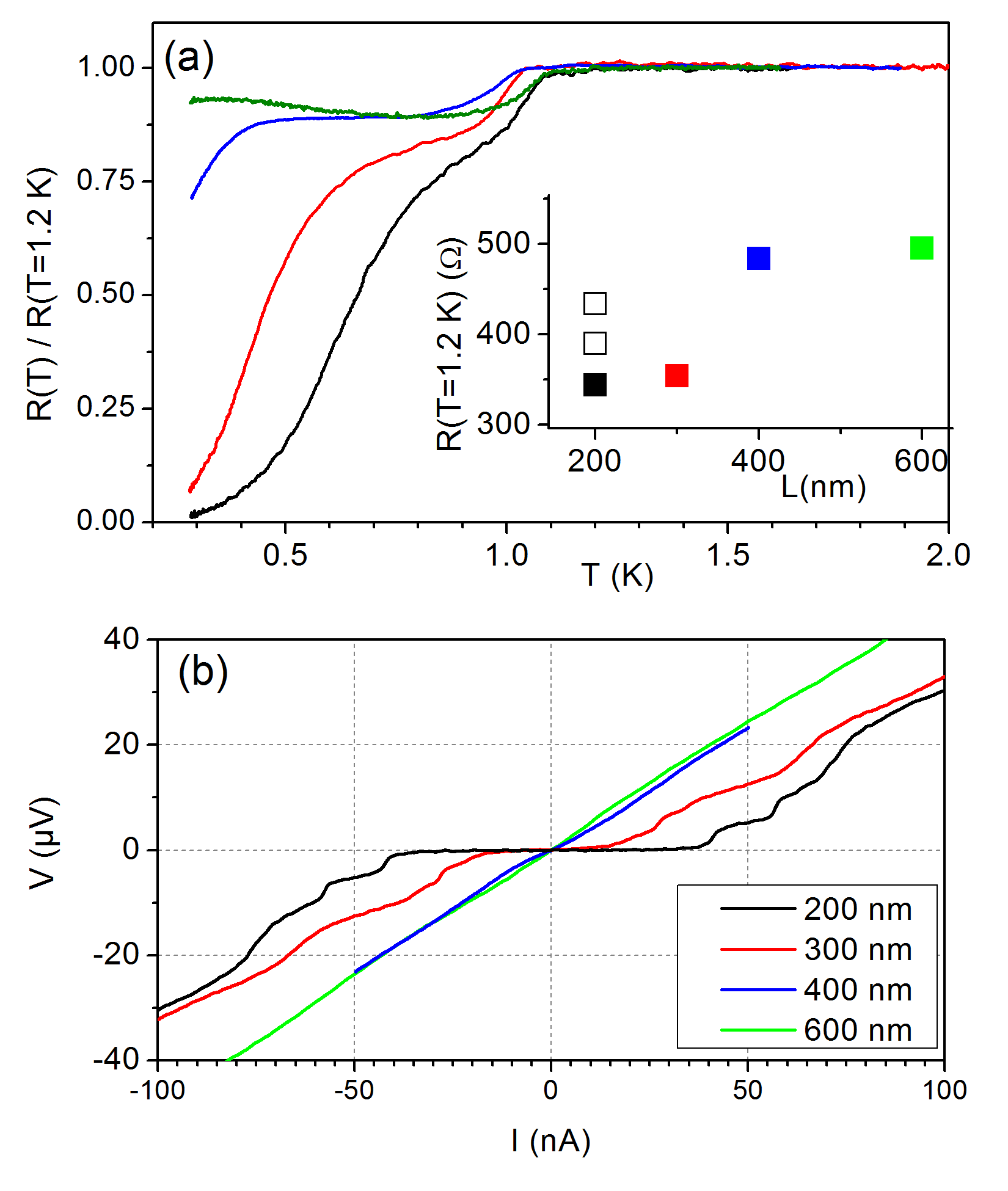
The temperature dependence of the resistance of four junctions is presented in Fig. 2(a). There is a kink at about 1 K monitoring the transition to superconductivity of the Ti/Al contacts. The junction with nm (green curve), appears to be going insulating. Not even in the smallest junctions with nm (black curve) and nm (red curve) is the transition to the superconducting state complete above 280 mK. The precursory effects of the dissipationless conductance in these junctions will be discussed elsewhere. Here we show that, no matter that some residual resistance is present above 280 mK, these junctions attain phase coherence and Josephson conduction. Fig. 2(b) shows the corresponding characteristics taken at mK for the four junctions presented in panel (a). The characteristic is practically ohmic for the junction with nm. A Josephson critical current and nA can be read off for the junctions with nm and nm respectively. The small steps at finite voltage below the Ti/Al gap can be attributed to localized subgap states (see below). The mean free path of graphene on hydrogenated SiC is estimated to be nm from room temperature measurements and the carrier density and mobility are only weakly modified from room temperature to liquid Helium temperature[26, 24]. Thus even the smallest of the junctions should be diffusive. Estimating the aluminium gap eV from conductance measurements (see Fig. 4(a)), we obtain a superconducting coherence length – nm, where is the diffusion constant. Hence our junctions with nm are in the crossover between the short and the long junction limit. A reduction of the Josephson critical current is expected in the long junction limit, as confirmed by the experiment.
For the nm junction, the product is smaller than the theoretical estimate[27] derived for junctions in which the Thouless energy is . This is the upper limit of the difference, since it is calculated for at ( is the critical temperature of the electrodes). The measured critical current density nA m-1 at nm falls in the range of the values reported in the literature, i.e. between 1 and 100 nA m-1, when the temperature is normalized to of the electrodes[28, 7, 29, 2].
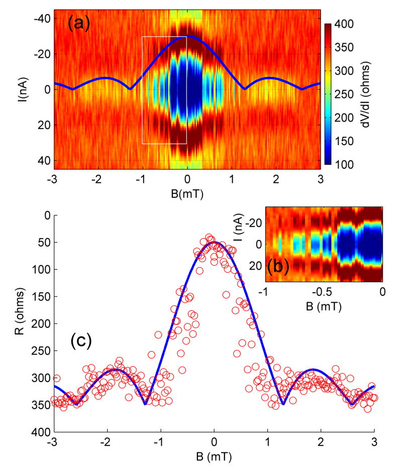
One of the most direct evidence of a genuine Josephson coupling is provided by a modulation of with a magnetic field which is applied perpendicularly to the substrate. The magnetic field dependence of the measured differential resistance for the nm junction is reported in Fig. 3(a). Experimentally, there is also a one to one correspondence between the magnitude of the Josephson critical current and the small residual resistance. Consequently, a similar magnetic pattern is retrieved from the magnetic field dependence of at , see panel (c). In panels (a,c), we have added for reference a conventional Fraunhofer interference curve:
where is the flux quantum. The one displayed here corresponds to an effective area m2. As the width of the junction is 4 m and the length 300 nm one could infer that the critical current density is homogeneous across the junction and that the physical area of the junction is involved, with the addition of some small penetration of the magnetic field in the Al/Ti contacts. However the sample, including the Al/Ti contacts, is a planar structure in the thin film limit and the field penetration in the Al/Ti contacts is expected to be large. In fact, a conventional Fraunhofer pattern only gives a qualitative envelope of a strongly oscillating pattern that is observed.
Fig. 3, panel (b) is an enlargement of these low fields oscillations. They are quasi periodic, with a pseudo-period of – Gauss which corresponds to a much larger effective area of m2. To account for a more extended flux penetration in the contacts, we have numerically calculated the macroscopic magnetic vector potential profile by solving the London equation, following a method originally employed by Rosenthal et al.[30, 31, 32] for planar junctions. The oscillations with the period of 3 Gauss and their enveloppe can be reproduced in this way by choosing a Pearl penetration length within the contacts m and a non uniform critical current density across the junction. However, a macroscopic London picture is still not fully convincing as the aperiodicity of the fast oscillating pattern, the residual resistance (see Fig. 3(c)) and some (fully reproducible) dependence on the sweeping of the applied magnetic field imply additional phenomena which cannot be accounted for within the macroscopic Rosenthal model. Most likely, vortex pinning in the Al/Ti contacts takes also place, as many impurities and pinning centers are expected to diffuse in the contacts during the deposition process. The fast oscillations in the pattern could be due to a non-uniform critical current density distribution[33, 34]. A more detailed account on the magnetic field dependence of will be given elsewhere[35].
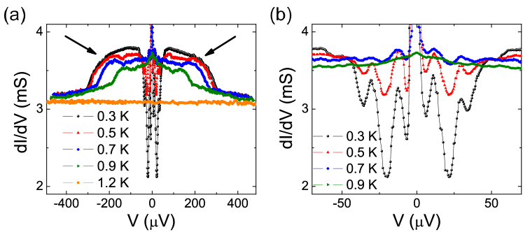
When investigating the behavior of the Al/Ti contacts further, by monitoring the conductance measurements for different temperatures reported in Fig. 4, we can identify the Al/Ti gap, with a marked temperature dependence (panel (a)), and few subgap structures which give rise to the steps in the characteristics at finite voltage, see Fig. 2(b). Temperature seems not to have any effect on these subgap structures, as shown in Fig. 4(b). This rules out the possibility that they originate from multiple Andreev reflection (MAR)[3]. This can be explained by considering that the interfaces with the contacts are expected to be rather rough. Poor transmission between the metallic aluminium contacts and the underlying graphene layer, responsible for a sizeable contact resistance, has also been found in the case of diffusive graphene transistors[36]. Possible origin of the subgap resonances could be resonant tunneling via localized states or even edge states in the graphene barrier. This feature will be investigated further in the future.
Uncovering the structure of the Al/Ti contacts in these devices is of the utmost relevance. Graphene and the Ti/Al contacts have a large work function difference and graphene may become -doped by charge transfer from the Al/Ti contact[37]. As graphene on the hydrogenated SiC interface is intrinsically -doped, devices could be engineered in the form of -- junctions. A Fabry-Pérot resonating transmission which has been found in perfect ballistic -- junctions[38] can be ruled out here, as our junctions are diffusive and the interfaces with the contact have low transparency. Still, this may be improved, as the mobility of G/SiC is known to increase strongly when the carrier concentration decreases.
4 Conclusion
Looking from the point of view of the graphene community, efforts have been mostly driven towards the realization of samples achieving a) a ballistic transport regime to exploit the unique properties of Andreev reflection in graphene[39, 40, 28, 41]; b) a more efficient control of charge density, with the possibility of reaching the neutrality point through electrostatic gate[42, 43]. The possible use of graphene junctions in real circuits is hindered, however, by the substantial limit of a technology that cannot produce a large number of junctions patterned on a single graphene flake with similar properties, thus controlling the electrodynamics and functionality of each of them, as well as of the global circuit.
This work demonstrates the Josephson conduction at subKelvin temperature, in various co-planar structures on one single monolayer of graphene and patterned Al superconducting contacts. Graphene is grown by CVD on SiC. The Josephson coherence appears to be highly reproducible, isotropic with respect to the substrate orientation and easily scalable with present standard lithographic techniques. These results have an immediate applicative impact opening up to a systematic comparative study where single constructive parameters of the graphene junctions can be selectively changed and barriers can be appropriately engineered.
5 Acknowledgements
Discussions with Piet Brouwer and Victor Rouco Gomez are gratefully acknowledged. Work supported by PICS CNRS-CNR 2014-2016 ”Transport phenomena and Proximity-induced Superconductivity in Graphene junctions”, Swedish Foundation for Strategic Research (SSF) under the project ”Graphene based high frequency electronics”, FIRB ”HybridNanoDev RBFR1236VV” (Italy) and by EU FP7, under grant agreement no 604391 Graphene Flagship.
References
- [1] Hubert B. Heersche, Pablo Jarillo-Herrero, Jeroen B. Oostinga, Lieven M. K. Vandersypen, and Alberto F. Morpurgo. Solid State Communications, 143(1-2):72, 2007.
- [2] H. B. Heersche, P. Jarillo-Herrero, J. B. Oostinga, L. M. K. Vandersypen, and A. F. Morpurgo. Bipolar supercurrent in graphene. Nature, 446:56, 2007.
- [3] Xu Du, Ivan Skachko, and Eva Y. Andrei. Phys. Rev. B, 77:184507, May 2008.
- [4] C. Ojeda-Aristizabal, M. Ferrier, S. Guéron, and H. Bouchiat. Phys. Rev. B, 79:165436, Apr 2009.
- [5] I. V. Borzenets, U. C. Coskun, S. J. Jones, and G. Finkelstein. Phys. Rev. Lett., 107(13):137005, 2011.
- [6] Gil-Ho Lee, Dongchan Jeong, Jae-Hyun Choi, Yong-Joo Doh, and Hu-Jong Lee. Phys. Rev. Lett., 107(14):146605, 2011.
- [7] M. Popinciuc, V. E. Calado, X. L. Liu, A. R. Akhmerov, T. M. Klapwijk, and L. M. K. Vandersypen. Phys. Rev. B, 85(20):205404, 2012.
- [8] U. C. Coskun, M. Brenner, T. Hymel, V. Vakaryuk, A. Levchenko, and A. Bezryadin. Phys. Rev. Lett., 108(9):097003, 2012.
- [9] X. S. Li, W. W. Cai, J. H. An, S. Kim, J. Nah, D. X. Yang, R. Piner, A. Velamakanni, I. Jung, E. Tutuc, S. K. Banerjee, L. Colombo, and R. S. Ruoff. Large-area synthesis of high-quality and uniform graphene films on copper foils. Science, 324(5932):1312, 2009.
- [10] J. Kedzierski, Pei-Lan Hsu, P. Healey, P.W. Wyatt, C.L. Keast, Mike Sprinkle, C. Berger, and Walt A. de Heer. IEEE Transactions on Electron. Devices, 55(8):2078, Aug 2008.
- [11] Jack Chan, Archana Venugopal, Adam Pirkle, Stephen McDonnell, David Hinojos, Carl W. Magnuson, Rodney S. Ruoff, Luigi Colombo, Robert M. Wallace, and Eric M. Vogel. Reducing extrinsic performance-limiting factors in graphene grown by chemical vapor deposition. ACS Nano, 6(4):3224–3229, 2012. PMID: 22390298.
- [12] Shinichi Tanabe, Yoshiaki Sekine, Hiroyuki Kageshima, Masao Nagase, and Hiroki Hibino. Phys. Rev. B, 84:115458, Sep 2011.
- [13] F. Lafont, R. Ribeiro-Palau, D. Kazazis, A. Michon, O. Couturaud, C. Consejo, T. Chassagne, M. Zielinski, M. Portail, B. Jouault, F. Schopfer, and W. Poirier. Nature Communications, 6:6806, 2015.
- [14] R. Ribeiro Palau, F. Lafont, J. Brun Picard, D. Kazazis, A. Michon, F Cheynis, O. Couturaud, C. Consejo, B. Jouault, W. Poirier, and F. Schopfer. Nature Nano., advance online publication, 2015.
- [15] W. Poirier, F. Lafont, S. Djordjevic, F. Schopfer, and L. Devoille. Journal of Applied Physics, 115(4):044509, 2014.
- [16] Katsuyoshi Komatsu, Chuan Li, S. Autier-Laurent, H. Bouchiat, and S. Guéron. Phys. Rev. B, 86:115412, Sep 2012.
- [17] Kang Li, Xiao Feng, Wenhao Zhang, Yunbo Ou, Lianlian Chen, Ke He, Li-Li Wang, Liwei Guo, Guodong Liu, Qi-Kun Xue, and Xucun Ma. Appl. Phys. Lett., 103(6):062601, 2013.
- [18] B. M. Ludbrook, G. Levy, P. Nigge, M. Zonno, M. Schneider, D. J. Dvorak, C. N. Veenstra, S. Zhdanovich, D. Wong, P. Dosanjh, C. Straßer, A. Stöhr, S. Forti, C. R. Ast, U. Starke, and A. Damascelli. Proceedings of the National Academy of Sciences, 112(38):11795, 2015.
- [19] A. P. Tiwari, S. Shin, E. Hwang, S.-G. Jung, T. Park, and H. Lee. ArXiv e-prints, August 2015.
- [20] Zheng Han, Adrien Allain, Hadi Arjmandi-Tash, Konstantin Tikhonov, Mikhail Feigel’man, Benjamin Sacepe, and Vincent Bouchiat. Nature Physics, 10(5):380, 2014.
- [21] Nicolas Camara, Jean-Roch Huntzinger, Gemma Rius, Antoine Tiberj, Narcis Mestres, Francesc Pérez-Murano, Philippe Godignon, and Jean Camassel. Phys. Rev. B, 80:125410, Sep 2009.
- [22] A. H. Castro Neto, F. Guinea, N. M. R. Peres, K. S. Novoselov, and A. K. Geim. Reviews of Modern Physics, 81(1):109, 2009.
- [23] A. Michon, S. Vézian, A. Ouerghi, M. Zielinski, T. Chassagne, and M. Portail. Appl. Phys. Lett., 97(17):171909, 2010.
- [24] B. Jabakhanji, A. Michon, C. Consejo, W. Desrat, M. Portail, A. Tiberj, M. Paillet, A. Zahab, F. Cheynis, F. Lafont, F. Schopfer, W. Poirier, F. Bertran, P. Le Fèvre, A. Taleb-Ibrahimi, D. Kazazis, W. Escoffier, B. C. Camargo, Y. Kopelevich, J. Camassel, and B. Jouault. Phys. Rev. B, 89:085422, Feb 2014.
- [25] L. Longobardi, D. Massarotti, G. Rotoli, D. Stornaiuolo, P. Papari, A. Kawakami, G.P. Pepe, A. Barone, and 10.1103/PhysRevB.84.184504F. Tafuri. Phys. Rev.B, 84:184504, 2011.
- [26] F. Speck, J. Jobst, F. Fromm, M. Ostler, D. Waldmann, M. Hundhausen, H. B. Weber, and Th. Seyller. Appl. Phys. Lett., 99(12):122106, 2011.
- [27] P. Dubos, H. Courtois, B. Pannetier, F. K. Wilhelm, A. D. Zaikin, and G. Schön. Phys. Rev. B, 63:064502, Jan 2001.
- [28] V. E. Calado, S. Goswami, G. Nanda, M. Diez, A. R. Akhmerov, K. Watanabe, T. Taniguchi, T. M. Klapwijk, and L. M. K. Vandersypen. Nature nanotechnology, 10(9):761, 2015.
- [29] Dongchan Jeong, Jae-Hyun Choi, Gil-Ho Lee, Sanghyun Jo, Yong-Joo Doh, and Hu-Jong Lee. Phys. Rev. B, 83:094503, Mar 2011.
- [30] Peter A. Rosenthal, M. R. Beasley, K. Char, M. S. Colclough, and G. Zaharchuk. Appl. Phys. Lett., 59(26):3482, 1991.
- [31] Francesco Tafuri and John R Kirtley. Reports on Progress in Physics, 68(11):2573, 2005.
- [32] R. Arpaia, M. Arzeo, S. Nawaz, S. Charpentier, F. Lombardi, and T. Bauch. Appl. Phys. Lett., 104(7):072603, 2014.
- [33] Antonio Barone and Gianfranco Paternò. Physics and applications of the Josephson effect. Wiley, 1982.
- [34] Sean Hart, Hechen Ren, Timo Wagner, Philipp Leubner, Mathias Mühlbauer, Christoph Brüne, Hartmut Buhmann, Laurens W. Molenkamp, and Amir Yacoby. Nature Physics, 10:638, 2014.
- [35] D. Masarotti et al., to be published.
- [36] Yanqing Wu, Vasili Perebeinos, Yu ming Lin, Tony Low, Fengnian Xia, and Phaedon Avouris. Nano Lett., 12(3):1417, 2012.
- [37] G. Giovannetti, P. A. Khomyakov, G. Brocks, V. M. Karpan, J. van den Brink, and P. J. Kelly. Phys. Rev. Lett., 101:026803, Jul 2008.
- [38] M. T. Allen, O. Shtanko, I. C. Fulga, J. I.-J. Wang, D. Nurgaliev, K. Watanabe, T. Taniguchi, A. R. Akhmerov, P. Jarillo-Herrero, L. S. Levitov, and A. Yacoby. ArXiv e-prints, June 2015.
- [39] M. Ben Shalom, M. J. Zhu, V. I. Fal’ko, A. Mishchenko, A. V. Kretinin, K. S. Novoselov, C. R. Woods, K. Watanabe, T. Taniguchi, A. K. Geim, and J. R. Prance. Nature Physics, 2015.
- [40] Naomi Mizuno, Bent Nielsen, and Xu Du. Nature Communications, 4:2716, 2013.
- [41] J. Baringhaus, M. Ruan, F. Edler, A. Tejeda, M. Sicot, A. Taleb-Ibrahimi, A. P. Li, Z. G. Jiang, E. H. Conrad, C. Berger, C. Tegenkamp, and W. A. de Heer. Nature, 506(7488):349, 2014.
- [42] Fabio Deon, Sandra Šopić, and Alberto F. Morpurgo. Phys. Rev. Lett., 112:126803, Mar 2014.
- [43] Jae-Hyun Choi, Gil-Ho Lee, Sunghun Park, Dongchan Jeong, Jeong-O. Lee, H. S. Sim, Yong-Joo Doh, and Hu-Jong Lee. Nature Communications, 4:2525, 2013.