Current address: ]Institute of Science and Technology Austria (IST Austria), 3400 Klosterneuburg, Austria
Superconducting cavity-electromechanics on silicon-on-insulator
Abstract
Fabrication processes involving anhydrous hydrofluoric vapor etching are developed to create high- aluminum superconducting microwave resonators on free-standing silicon membranes formed from a silicon-on-insulator wafer. Using this fabrication process, a high-impedance GHz coil resonator is coupled capacitively with large participation ratio to a MHz micromechanical resonator. Two-tone microwave spectroscopy and radiation pressure back-action are used to characterize the coupled system in a dilution refrigerator down to temperatures of mK, yielding a measured electromechanical vacuum coupling rate of Hz and a mechanical resonator -factor of . Microwave back-action cooling of the mechanical resonator is also studied, with a minimum phonon occupancy of phonons being realized at an elevated fridge temperature of mK.
Recent work in the field of cavity-optomechanics has shown the feasibility of using radiation pressure to cool micromechanical objects close to their quantum ground state Teufel et al. (2011); Chang et al. (2011), to measure the quantum motion of such objects Safavi-Naeini et al. (2012); Weinstein et al. (2014), and to prepare non-classical mechanical states using back-action evading techniques Wollman et al. (2015); Pirkkalainen et al. (2015); Lecocq et al. (2015). In a dual role, mechanical objects may be used to create large electromagnetic nonlinearities for slowing Weis et al. (2010); Chang et al. (2011); Safavi-Naeini et al. (2011); Teufel et al. (2011), squeezing Safavi-Naeini et al. (2013); Purdy et al. (2013), or even shifting the frequency of light Hill et al. (2012). These experiments have utilized either optical or microwave photons to induce radiation pressure forces, though recent work has coupled opto- and electro-mechanical systems and realized reversible microwave-to-optical conversion Andrews et al. (2014). An outstanding problem in the field is to realize such conversion in a fully integrated, on-chip platform Davanço et al. (2012); Pitanti et al. (2015).
Here, we develop a new fabrication process for the creation of high- microwave superconducting aluminum (Al) resonators on thin-film silicon membranes suitable for integration with mechanical and photonic devices. As a proof of concept, we demonstrate parametric radiation pressure coupling of an GHz microwave superconducting resonator to the motion of a MHz silicon micromechanical resonator. The electromechanical circuit, shown schematically in Fig. 1(a), consists of a high-impedance microwave coil resonator capacitively coupled to the fundamental in-plane differential mode of a pair of patterned silicon slabs. Although not a feature exploited in the present study, the patterned slabs also form a slotted photonic crystal cavity which supports an optical resonance in the nm telecom wavelength band Safavi-Naeini et al. (2010); Winger et al. (2011); Pitanti et al. (2015). In principle, this mechanical resonator (what we hereafter refer to as the “H-slot” resonator) could simultaneously couple to optical photons in the photonic crystal cavity and microwave photons in the superconducting microwave resonator.
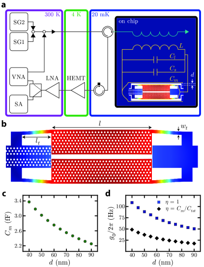
The H-slot mechanical resonator is depicted in Fig. 1(b), where finite-element method (FEM) numerical simulations COM are used to solve for the fundamental in-plane mechanical motion of the structure. The resonator is formed from a Si layer of nm thickness, and consists of two patterned slabs that are separated by a central nanoscale slot and tethered on each end to a central clamp point. As mentioned, the hole patterning in the two slabs produces a localized photonic crystal cavity. The hole patterning on the left side of the H-slot resonator forms a photonic crystal optical waveguide which can be used to efficiently excite the optical cavity. Aluminum electrodes are fed into the H-slot resonator from the right side of the structure, and span the outer edges of the two slabs forming one half of a vacuum gap capacitor [labeled in Fig. 1(a)]. The length ( m) of the photonic crystal slabs is chosen long enough to support a high- optical mode and to realize a motional capacitance on the scale of a few femtoFarad. The width () of the photonic crystal slabs is chosen to accommodate a number of photonic crystal periods that should (again) provide high optical , but otherwise is minimized to limit the motional mass of the resonator. The slab photonic crystals are supported by tethers whose length ( m) and width ( nm) produce a simulated mechanical frequency of MHz for the fundamental in-plane differential mode, compatible with resolved-sideband pumping through the coupled microwave circuit.
The simulated effective mass and zero-point amplitude of the differential mode are pg and fm, respectively. These figures include the aluminum wires (width nm, thickness nm) that form the vacuum gap capacitor. By using a tuning fork design in which the upper and lower slabs are coupled together at each end through the central tether clamp points, acoustic radiation out the ends of H-slot resonator can be greatly reduced. Optimization of the tether clamp point geometry yields a numerically simulated mechanical quality factors as high as .
The vacuum electromechanical coupling rate of the H-slot mechanical resonator to the microwave coil resonator is given by,
| (1) |
where is the generalized amplitude coordinate of the fundamental in-plane differential mode of interest, is the zero-point amplitude of the mechanical resonance, is the participation ratio of the motional capacitance () to the total capacitance of the circuit (). In addition to the motional capacitance, the total circuit capacitance consists of the intrinsic self-capacitance of the inductor coil () and any additional stray capacitance of the circuit (). This ratio - and hence the electromechanical coupling - is maximized for small and large . We achieve a relatively small value of coil capacitance by using a tightly wound rectangular spiral inductor Mohan et al. (1999); Fink et al. (2015) with wire width of nm and wire-to-wire pitch of m. A simulation of the entire circuit layout, including nearby ground-plane, coupling wire, and connecting wires between the coil and the motional capacitor yields an additional stray capacitance of fF. For a coil of turns, with an estimated inductance of nH and capacitance fF, connected in parallel to a motional capacitance of fF corresponding to a vacuum gap of nm, the microwave resonance frequency of the coupled circuit is estimated to be GHz. Using these circuit parameters in conjunction with a perturbative calculation Eichenfield et al. (2009); Pitanti et al. (2015) of based upon FEM simulations of the differential mechanical mode and the electric field distribution in the vacuum gap capacitor, yields a calculated vacuum electromechanical coupling strength of Hz. The trend of both and with gap size are shown in Fig. 1(c).
The devices studied in this work are fabricated from cm cm chips diced from a high-resistivity silicon-on-insulator (SOI) wafer manufactured by SOITEC using the Smart Cut process SOI . The SOI wafer consists of a nm thick silicon device layer with (100) surface orientation and -type (Boron) doping with a specified resistivity of -cm. Underneath the device layer is a m buried silicon dioxide () BOX layer. The device and BOX layers sit atop a silicon (Si) handle wafer of thickness m and a specified resistivity of -cm. Both the Si device layer and handle wafer are grown using the Czochralski crystal growth method.
Fabrication of the coupled coil resonator and H-slot resonator can be broken down into the following six steps. In step (1), we pattern the H-slot resonator using electron beam (e-beam) lithography in ZEP-520A resist, and etch this pattern into the Si device layer using an inductively coupled plasma reactive ion etch (ICP-RIE). After the ICP-RIE etch, we clean the chips with a min piranha bath and a sec buffered hydrofluoric acid (BHF) dip. In step (2), we pattern the capacitor electrodes and ground plane region using ZEP-520A resist and use electron beam evaporation to deposit nm of Al on the chip. In step (3), we define a protective scaffold formed out of LOR 5B e-beam resist to create the crossover regions of the spiral inductor coil. In step (4), we pattern the inductor coil wiring in a double stack of PMMA 495 and PMMA 950 resists and deposit nm of Al using electron beam evaporation. In step (5), we define a metal contact region that connects the wiring between the capacitor electrodes and the inductive coil, then perform a min ion mill before evaporating nm of Al. After all metal layer depositions, we perform a lift-off process for h in N-Methyl-2-pyrrolidone at 150oC.
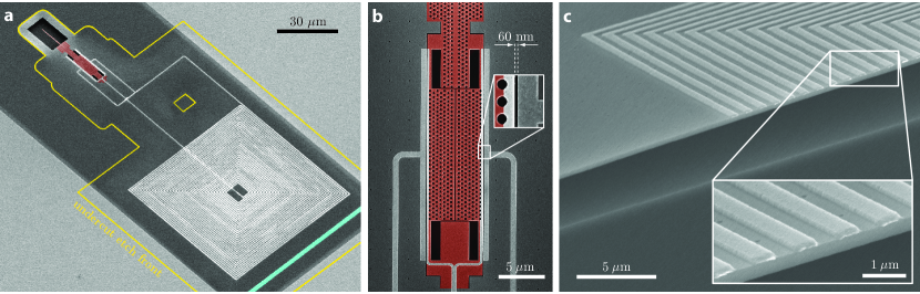
In a final step (6), we release the structure by using an anhydrous vapor hydrofluoric (HF) acid etch using the SPTS uEtch system. This etch is used to selectively remove the underlying BOX layer without attacking the Al metal or Si device layers. Not only is the removal of the BOX layer desirable from the standpoint of allowing the mechanical structure to move, but we have found that the presence of the underlying BOX layer results in a significant amount of electrical loss in the microwave resonator. Measurements of both co-planar waveguide and lumped element microwave resonators have shown that the microwave -factor is substantially degraded (resonances difficult to detect; ) with the BOX layer present. Stripping off the Si device layer and forming microwave resonators directly on the BOX layer marginally improves the microwave -factor (), whereas stripping off both the device layer and BOX layer realize microwave resonators with when fabricated directly on the Si handle wafer. The release of the structure is facilitated by patterning an array of small ( nm diameter) holes into the Si device layer during step (1). The array of release holes are on a m pitch and cover the region containing the coil and H-slot resonator. A timed etch of min is used to remove 6 m of , resulting in complete removal of the BOX layer underneath the microwave circuit. A scanning electron microscope (SEM) image of the fully released structure is shown in Fig. 2(a). Zoom-in images of the H-slot mechanical resonator and undercut inductor coil are shown in Figs. 2(b) and (c), respectively.
Electromechanical measurements of the fabricated coil resonator are performed in a dilution refrigerator down to a temperature of mK. Microwave signals are launched onto the SOI chip using a co-planar waveguide. The co-planar waveguide is terminated by extending the center conductor with a m wide wire and then shorting it into ground. The wire is passed within m of the side of the inductor coil [see Fig. 2(a)], thus providing large inductive coupling to the microwave resonator. A region extending roughly m from the edge of the surrounding ground plane of the co-planar waveguide an inductive coupling wire is also undercut and the BOX layer fully removed. Read-out of the reflected microwave signal is performed using the measurement scheme shown in Fig. 1(a). The input line is thermalized at each stage of the fridge with a series of attenuators to eliminate Johnson thermal noise from the room temperature environment, yielding a calibrated input line attenuation of dB. The reflected signal is redirected using a pair of circulators at the mixing chamber stage of the fridge and then sent into an amplifier chain consisting of a HEMT amplifier at the K fridge stage and a low-noise amplifier at room temperature. The total amplifier gain is dB with an equivalent added microwave noise photon number of .
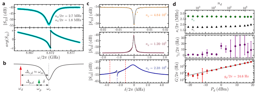
Figure 3(a) shows the measured magnitude and phase of the reflected microwave signal versus frequency from a vector network analyzer (VNA) used to probe the electrical properties of the device. The microwave resonance frequency is measured to be GHz, in close correspondence to the resonance frequency based upon the simulated values of the coil inductance and the motional and stray capacitance of the circuit. At the lowest base temperature of our fridge, mK, we measure an intrinsic microwave cavity loss rate of MHz at an intra-cavity photon number on resonance of , corresponding to an internal quality factor of . The external coupling rate to the resonator is measured to be MHz, putting the device well into the overcoupled regime. We note that for similar coil resonators (without an H-slot resonator and coil cross-overs) which were coupled more weakly using a transmission as opposed to reflection geometry, we have observed internal quality factors as high as , close to the measured -values for resonators fabricated directly on the Si handle wafer. Further investigation is needed to determine the source of the additional microwave loss in the electro-mechanical devices studied here.
To characterize the mechanical properties of the H-slot resonator, and to determine the strength of its radiation pressure coupling to the microwave coil resonator, we perform two-tone pump and probe measurements as illustrated in Fig. 3(b). Here, a strong drive tone of power is applied at frequency on the red motional sideband of the microwave cavity resonance while a weak probe tone is scanned across the cavity resonance. Interference between the anti-Stokes sideband of the drive tone and the weak probe tone results in a form of mechanically-mediated electromagnetically-induced transparency (EIT) Weis et al. (2010); Chang et al. (2011); Teufel et al. (2011); Safavi-Naeini et al. (2011), which for pump detuning near two-photon resonance () yields a reflection spectrum given by,
| (2) |
where is the detuning of the probe frequency () from the cavity resonance (), and is the total loaded cavity damping rate. Here we have made approximations assuming the system is sideband resolved () and that the probe signal is weak enough so as to not saturate the drive tone Safavi-Naeini et al. (2011).
A subset of the measured spectra over a range of drive powers are shown in Fig. 3(c) around the EIT transparency window. The drive detuning at two-photon resonance corresponds to the mechanical resonance frequency, and is found to be MHz, very close to the numerically simulated resonance frequency of the in-plane differential mode of the H-slot resonator. The cooperativity associated with the coupling of the microwave cavity field to the mechanical resonator is given by , where is the back-action-induced damping of the mechanical resonator by the microwave drive tone. At low drive powers corresponding to , we observe a narrow dip at the center of the broad microwave cavity resonance. As the drive power is increased and the dip becomes a peak in the reflected signal and the bandwidth of the transparency window increases with pump power. At the highest powers we observe a substantially broadened transparency window, where we observe the presence of a second, spurious mechanical resonance about kHz below that of the strongly coupled resonance. We attribute this spurious resonance to weak hybridization of the extended membrane modes of the undercut SOI with the localized in-plane differential mode of the H-slot resonator.
Ignoring the spurious mechanical mode, we fit the measured EIT spectra using Eq. (2) and extract the microwave cavity parameters (, , ), the intrinsic mechanical damping (), the mechanical resonance frequency (), and the parametrically-enhanced electromechanical coupling rate (). Figure 3(d) plots each of these fit parameters versus drive power and intra-cavity drive photon number (). is found to weakly rise with , most likely due to heating of the SOI membrane resulting from absorption of the microwave pump. For intra-cavity photon number , we no longer observe a microwave resonance, suggesting that absorption of the microwave pump causes the superconducting circuit to go normal. Fitting the measured curve of versus pump photon number yields an estimate for the vacuum electromechanical coupling rate of Hz, in good correspondence with the simulated value of Hz. The slight discrepancy is likely attributable to an under-estimation of the true capacitor gap size due to overhang of the Al electrode into the gap. For a nm dielectric gap, consistent with an additional nm overhang of Al estimated from cross-sectional images of similar devices, the simulated vacuum coupling rate drops to Hz
At low drive powers, the EIT transparency window bandwidth is dominated by the intrinsic mechanical linewidth, . However, we observe a frequency jitter of the mechanical resonance frequency. The range of the frequency jitter is of the order of several Hz on the second timescale, and saturates at approximately Hz for timescales on the order of tens of minutes. The source of the mechanical frequency jitter is unknown, but may be related to the excess heating we observe at the lowest fridge temperatures as described below. The resolution bandwidth of the VNA is also limited to Hz, and combined with the frequency jitter leads to significant distortion and blurring of the measured EIT spectrum at low drive power as can be seen in the top plot of Fig. 3(c). Estimates of and the corresponding cooperativity are thus unreliable from the EIT spectra alone.
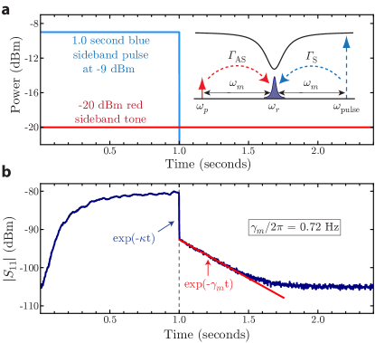
To directly measure the intrinsic damping rate we perform a mechanical ring-down measurement as shown in Fig. 4. Here, a strong blue-detuned pulse tone at frequency is applied for s to amplify the thermal mechanical motion of the mechanical resonator through dynamic back-action Kippenberg et al. (2005); Grudinin et al. (2010); Cohen et al. (2015). A weak red-detuned probe tone at is applied to the microwave cavity in order to read-out the phonon occupancy of the resonator after the blue detuned pulse is turned off. A spectrum analyzer with resolution bandwidth set to RBW kHz is used to measure the motionally scattered photons near the cavity resonance from the pulse and probe tones, providing a time domain signal proportional to the mechanical resonator phonon occupancy as shown in Fig. 4(b).
Fitting the decay of the spectrum analyzer signal after the pulse tone is turned off, and after the initial rapid decay of pulse photons from the cavity, yields a mechanical damping rate of Hz. Note that as the probe tone power of dBm corresponds to an intra-cavity photon number of only , the dynamic back-action damping of the probe is small but non-negligible at Hz. The corresponding intrinsic mechanical damping rate is thus approximately, Hz, corresponding to a mechanical quality factor of .
The red-sideband pump configuration () used to measure the EIT spectra also cools the mechanical resonator. Using a spectrum analyzer to measure the anti-Stokes scattered drive photons near the microwave cavity resonance, as shown schematically in Fig. 5(a), and calibrating the measured noise spectrum allows one to infer the average (noise/thermal) phonon occupancy () of the mechanical resonator as a function of the drive power. This sort of mechanical mode thermometry Teufel et al. (2011); Fink et al. (2015) at the lowest fridge temperature of mK shows large fluctuations in the inferred mechanical mode temperature ( mK), as a function of both time and drive power. The source of this anomalous mechanical mode heating is not well understood at this point, but may be related to coupling between the driven microwave resonator and two-level systems (TLS) Gao (2008) present in the native oxide on the surface of the Si device Gao et al. (2008); Wisbey et al. (2010); Bruno et al. (2015). TLS can not only absorb energy from the microwave drive, but also may hybridize with the microwave cavity and influence the transduction of mechanical motion yielding artificially high or low inferred mechanical mode occupancy Fink et al. (2015).
To better characterize the back-action cooling of the mechanics, we performed a cooling sweep at a fridge temperature of mK, where the anomalous heating effects seen at mK are less significant in comparison to the thermal bath of the fridge. A plot of the inferred mechanical mode occupancy () and corresponding mode temperature () versus the drive power applied on the red-sideband () is shown in Fig. 5(b). At low drive powers where and back-action cooling is expected to be negligible, we find that the mechanics thermalizes to an occupancy very close to the mechanical thermal occupancy at the fridge temperature, . For comparison a plot of the ideal cooling curve, , due to radiation pressure back-action is shown as a dashed curve in Fig. 5(b). Here we use an intrinsic damping rate ( Hz) and vacuum coupling rate ( Hz) inferred from EIT measurements at mK. The measured mechanical mode occupancy is in good agreement with theory, except at powers dBm where we again observe anomalous heating effects. Nonetheless, we are able to perform well over a decade of cooling and reach occupancies as low as .
In addition to the measured Lorentzian noise peak of the mechanical resonance, we also observe broadband noise which increases with the drive power. Figure 5(c) shows a plot of the measured broadband noise (back curve) at the highest intra-cavity drive photon number of . This broadband noise does not seem to be phase noise of our microwave source as addition of a narrowband input filter had no effect on the measured noise spectrum. Assuming that the noise is associated with an elevated electrical noise temperature of the device, we include both an input waveguide thermal noise occupancy () and a cavity thermal noise occupancy () to our model. Taking the waveguide and cavity to be at the same noise temperature (i.e., ) yields a flat reflection noise spectrum as shown in Fig. 5(c). Fitting the noise background at each drive power yields an estimate for the cavity and waveguide noise photon numbers, which are shown versus drive power as grey triangles in Fig. 5(b). The inferred effective noise temperature of the microwave cavity at the highest drive power is K, close to the critical temperature for Al Cochran and Mapother (1958) and consistent with the circuit going normal at higher drive powers.
Enhancement in the back-action cooling and electro-mechanical cooperativity of the current devices can be realized most straightforwardly through reduction in the microwave resonator loss. Significant reduction in the microwave loss and heating effects should be attainable through the use of higher resistivity Si Wisbey et al. (2010); Bruno et al. (2015). The vacuum electro-mechanical coupling rate may also be increased to Hz through optimization of the circuit layout to reduce stray capacitance and reduction of the capacitor gap to previously reported values of nm Pitanti et al. (2015). As the Si dielectric loss is reduced, and if one hopes to create highly coherent qubits on SOI Weber et al. (2011); Patel et al. (2013), TLS in the Si surfaces will need to be mitigated Gao et al. (2008); Wisbey et al. (2010); Bruno et al. (2015). In this regard, anhydrous vapor HF etching may be useful as it is compatible with numerous electron beam and photosensitive resists, thus allowing cleaning and hydrogen passivation of the Si surface right before and after critical fabrication steps of superconducting resonators and Josephson-Junction qubits Oliver and Welander (2013).
Looking forward, SOI represents a unique platform for integrating microwave, mechanical, and optical circuits. This is particularly interesting in the context of recent proposals and experimental efforts to utilize mechanical elements as quantum converters between microwave and optical light Safavi-Naeini et al. (2011); Wang and Clerk (2012); Bochmann et al. (2013); Andrews et al. (2014); Bagci et al. (2014); Černotík and Hammerer (2015). SOI is the substrate of choice for many nano- and micro-photonics applications due to the advanced fabrication techniques developed in Si and its excellent waveguiding and optical properties in the nm telecom wavelength band Bogaerts et al. (2005). SOI has also been successfully utilized in the development of thin-film optomechanical crystals, in which photonic and phononic bandgap effects are utilized to co-localize and strongly interact near-IR light with GHz-frequency phonons Eichenfield et al. (2009); Meenehan et al. (2015). Such a device architecture would allow for a fully integrated, scalable platform for on-chip quantum information processing and long-distance quantum networking Kimble (2008).
Acknowledgements.
The authors would like to thank Dan Vestyck at SPTS for performing trial HF vapor etch fabrication runs, and Barry Baker for his good humor and tireless effort to get the HF vapor etcher set up at Caltech. The authors also thank Alessandro Pitanti and Richard Norte for their contributions to initial fabrication development in SOI. This work was supported by the AFOSR through the “Wiring Quantum Networks with Mechanical Transducers” MURI program, the Institute for Quantum Information and Matter, an NSF Physics Frontiers Center with support of the Gordon and Betty Moore Foundation, and the Kavli Nanoscience Institute at Caltech. P.B.D. acknowledges support from a Barry Goldwater Scholarship.References
- Teufel et al. (2011) J. D. Teufel, D. Li, M. S. Allman, K. Cicak, A. J. Sirois, J. D. Whittaker, and R. W. Simmonds, Nature 471, 204 (2011).
- Chang et al. (2011) D. Chang, A. H. Safavi-Naeini, M. Hafezi, and O. Painter, New J. Phys. 13, 023003 (2011).
- Safavi-Naeini et al. (2012) A. H. Safavi-Naeini, J. Chan, J. T. Hill, T. P. M. Alegre, A. Krause, and O. Painter, Phys. Rev. Lett. 108, 033602 (2012).
- Weinstein et al. (2014) A. J. Weinstein, C. U. Lei, E. E. Wollman, J. Suh, A. Metelmann, A. A. Clerk, and K. C. Schwab, Phys. Rev. X 4, 041003 (2014).
- Wollman et al. (2015) E. E. Wollman, C. U. Lei, A. J. Weinstein, J. Suh, A. Kronwald, F. Marquardt, A. A. Clerk, and K. C. Schwab, Science 349, 952 (2015).
- Pirkkalainen et al. (2015) J. M. Pirkkalainen, E. Damskägg, M. Brandt, F. Massel, and M. A. Sillanpää, Phys. Rev. Lett. 115, 243601 (2015).
- Lecocq et al. (2015) F. Lecocq, J. Clark, R. Simmonds, J. Aumentado, and J. Teufel, Phys. Rev. X 5, 041037 (2015).
- Weis et al. (2010) S. Weis, R. Rivière, S. Deléglise, E. Gavartin, O. Arcizet, A. Schliesser, and T. J. Kippenberg, Science 330, 1520 (2010).
- Safavi-Naeini et al. (2011) A. H. Safavi-Naeini, T. P. M. Alegre, J. Chan, M. Eichenfield, M. Winger, Q. Lin, J. T. Hill, D. Chang, and O. Painter, Nature 472, 69 (2011).
- Safavi-Naeini et al. (2013) A. H. Safavi-Naeini, S. Gröblacher, J. T. Hill, J. Chan, M. Aspelmeyer, and O. Painter, Nature 500, 185 (2013).
- Purdy et al. (2013) T. P. Purdy, R. W. Peterson, and C. A. Regal, Science 339, 801 (2013).
- Hill et al. (2012) J. T. Hill, A. H. Safavi-Naeini, J. Chan, and O. Painter, Nature Commun. 3, 1196 (2012), 1206.0704 .
- Andrews et al. (2014) R. W. Andrews, R. W. Peterson, T. P. Purdy, K. Cicak, R. W. Simmonds, C. A. Regal, and K. Lehnert, Nature Physics 10, 321 (2014).
- Davanço et al. (2012) M. Davanço, J. Chan, A. H. Safavi-Naeini, O. Painter, and K. Srinivasan, Opt. Express 20, 24394 (2012).
- Pitanti et al. (2015) A. Pitanti, J. M. Fink, A. H. Safavi-Naeini, J. T. Hill, C. U. Lei, A. Tredicucci, and O. Painter, Opt. Express 23, 3196 (2015).
- Safavi-Naeini et al. (2010) A. H. Safavi-Naeini, T. P. M. Alegre, M. Winger, and O. Painter, Appl. Phys. Lett. 97, 181106 (2010).
- Winger et al. (2011) M. Winger, T. D. Blasius, T. P. M. Alegre, A. H. Safavi-Naeini, S. Meenehan, J. Cohen, S. Stobbe, and O. Painter, Opt. Express 19, 24905 (2011).
- (18) COMSOL Multiphysics 3.5, http://www.comsol.com/.
- Mohan et al. (1999) S. Mohan, M. del Mar Hershenson, S. Boyd, and T. Lee, Solid-State Circuits, IEEE Journal of 34, 1419 (1999).
- Fink et al. (2015) J. M. Fink, M. Kalaee, A. Pitanti, R. Norte, L. Heinzle, M. Davanco, K. Srinivasan, and O. Painter, arXiv:1512.04660 (2015).
- Eichenfield et al. (2009) M. Eichenfield, J. Chan, R. M. Camacho, K. J. Vahala, and O. Painter, Nature 462, 78 (2009).
- (22) SOITEC, http://www.soitec.com/.
- Kippenberg et al. (2005) T. Kippenberg, H. Rokhsari, T. Carmon, A. Scherer, and K. Vahala, Phys. Rev. Lett. 95, 033901 (2005).
- Grudinin et al. (2010) I. S. Grudinin, H. Lee, O. Painter, and K. J. Vahala, Phys. Rev. Lett. 104, 083901 (2010).
- Cohen et al. (2015) J. D. Cohen, S. M. Meenehan, G. S. MacCabe, S. Gröblacher, A. H. Safavi-Naeini, F. Marsili, M. D. Shaw, and O. Painter, Nature 520, 522 (2015).
- Gao (2008) J. Gao, The Physics of Superconducting Microwave Resonators, Ph.D. thesis, California Institute of Technology (2008).
- Gao et al. (2008) J. Gao, M. Daal, A. Vayonakis, S. Kumar, J. Zmuidzinas, B. Sadoulet, B. A. Mazin, P. K. Day, and H. G. Leduc, Appl. Phys. Lett. 92, 152505 (2008).
- Wisbey et al. (2010) D. S. Wisbey, J. Gao, M. R. Vissers, F. C. S. da Silva, J. S. Kline, L. Vale, and D. P. Pappas, J. Appl. Phys. 108, 093918 (2010).
- Bruno et al. (2015) A. Bruno, G. de Lange, S. Asaad, K. L. van der Enden, N. K. Langford, and L. DiCarlo, App. Phys. Lett. 106, 182601 (2015).
- Cochran and Mapother (1958) J. F. Cochran and D. E. Mapother, Phys. Rev. 111, 132 (1958).
- Weber et al. (2011) S. J. Weber, K. W. Murch, D. H. Slichter, R. Vijay, and I. Siddiqi, Appl. Phys. Lett. 98, 172510 (2011).
- Patel et al. (2013) U. Patel, Y. Gao, D. Hover, G. J. Ribeill, S. Sendelbach, and R. McDermott, App. Phys. Lett. 102, 012602 (2013).
- Oliver and Welander (2013) W. D. Oliver and P. B. Welander, MRS BULLETIN 38, 816 (2013).
- Wang and Clerk (2012) Y.-D. Wang and A. A. Clerk, New Journal of Physics 14, 105010 (2012).
- Bochmann et al. (2013) J. Bochmann, A. Vainsencher, D. D. Awschalom, and A. N. Cleland, Nature Physics 9, 712 (2013).
- Bagci et al. (2014) T. Bagci, A. Simonsen, S. Schmid, L. G. Villanueva, E. Zeuthen, J. Appel, J. M. Taylor, A. Sorensen, K. Usami, A. Schliesser, and E. S. Polzik, Nature 507, 81 (2014).
- Černotík and Hammerer (2015) O. Černotík and K. Hammerer, arXiv:1512.00768 (2015).
- Bogaerts et al. (2005) W. Bogaerts, R. Baets, P. Dumon, V. Wiaux, S. Beckx, D. Taillaert, B. Luyssaert, J. Van Campenhout, P. Bienstman, and D. Van Thourhout, Journal of Lightwave Technology 23, 401 (2005).
- Meenehan et al. (2015) S. M. Meenehan, J. D. Cohen, G. S. MacCabe, F. Marsili, M. D. Shaw, and O. Painter, Phys. Rev. X 5, 041002 (2015).
- Kimble (2008) H. J. Kimble, Nature 453, 1023 (2008).