Published in: PRB 93, 121202(R) (March 2016)
Interband optical conductivity of the [001]-oriented Dirac semimetal Cd3As2
Abstract
We measured the optical reflectivity of [001]-oriented -doped
Cd3As2 in a broad frequency range (50 –
22 000 cm-1) for temperatures from 10 to 300 K. The optical
conductivity, , is isotropic within the (001) plane; its real
part follows a power law, , in a large interval from 2000 to 8000 cm-1.
This behavior is caused by interband transitions between two Dirac
bands, which are effectively described by a sublinear dispersion
relation, . The
momentum-averaged Fermi velocity of the carriers in these bands is
energy dependent and ranges from to m/s, depending on the distance from the Dirac points. We
detect a gaplike feature in and associate it
with the Fermi level positioned around meV above the Dirac
points.
DOI: 10.1103/PhysRevB.93.121202
I Introduction
The interest in measurements of the optical conductivity, , in three-dimensional (3D) Dirac materials Wehling is triggered by the fact that the interband conductivity in these systems is expected to demonstrate a peculiar behavior. Generally, the interband optical response of -dimensional Dirac electrons is supposed to be universal: should follow a power-law frequency dependence,
| (1) |
where is the exponent in the band dispersion relation, , Hosur2012 ; Bacsi2013 .
For example, is proportional to frequency in the case of perfectly linear Dirac cones in three dimensions. Such linearity in over a broad frequency range in a 3D system is often considered as a “smoking gun” for Dirac physics (either of topological or of other origin, Orlita2014 ). For example, Timusk et al. Timusk2013 have claimed the presence of 3D Dirac fermions in a number of quasicrystals based entirely on the observation of a linear in these materials. Linear-in-frequency has also been found in ZrTe5 Chen2015 , where 3D linear bands are evidenced by transport and angle-resolved photoemission experiments Li2014 .
In 2013 Wang et al. Wang2013 predicted 3D topological Dirac points in Cd3As2; by now they are well confirmed by ARPES, scanning tunneling spectroscopy, and magnetotransport measurements Borisenko2014 ; Liu2014Nat ; Neupane2014 ; Jeon2014 ; He2014 ; Liang2015 . Due to the presence of inversion symmetry in Cd3As2, the bands are not spin polarized Ali2014 . The shape of the Dirac bands in Cd3As2 is somewhat complicated by the presence of a Lifshitz-transition point Jeon2014 ; see Fig. 1 for a sketch of the Dirac bands.
The goal of this report is to provide insight into the Dirac-band dispersion in Cd3As2 by means of optical spectroscopy. Previous optical investigations of Cd3As2 performed in the 70s and 80s can be divided into two groups. The first one Turner1961 ; Iwami1973 ; Gelten1980 ; GeltenPhD ; Houde1986 ; LB deals with the low-energy part of the optical spectra (usually, below some 250 meV, or 2000 cm-1) discussing mostly phonon modes and free-electron Drude-like absorption. Turner et al. Turner1961 identify a very narrow (130 meV) optical gap in the optical absorption. Another group of papers Zivitz ; Karnicka ; Sobolev1 ; Sobolev2 ; Kozlov mainly discusses absorption features at energies of a few electron volts and their relations to transitions between different (high-energy) parabolic bands. No optical conductivity was derived from these measurements.
Recent recognition of the nontrivial electron-band topology of Cd3As2 calls for a fresh look into its optical properties. In this paper, we report broadband optical investigations of Cd3As2.
II Experiment
Single crystals of Cd3As2 have been grown by vapor transport from material previously synthesized in argon flow Nateprov2015 , see Supplemental Material for details. Resistivity and Hall measurements provide an electron density of cm-3 (roughly independent of temperature), a metallic resistivity, and a mobility of cm2/Vs at 12 K.

The investigated Cd3As2 single crystal had lateral dimensions of 2.5 mm by 3 mm and a thickness of 300 m. It was cut out from a larger single crystal. The crystallographic axes of the sample were found by x-ray diffraction. The [001] axis was perpendicular to the sample’s largest surface. This surface was polished prior the optical measurements, which were performed for a few linear polarizations. The direct-current (dc) resistivity of this sample was characterized in-plane by standard four-probe method (inset of Fig. 5).
The optical reflectivity was measured at 10 to 300 K with light polarized along different crystallographic directions. The spectra in the far-infrared (50 cm-1 – 1000 cm-1) were recorded by a Bruker IFS 113v Fourier-transform infrared spectrometer using an in-situ gold overfilling technique for reference measurements gold . At higher frequencies (700 cm-1 – 22 000 cm-1) a Bruker Hyperion microscope attached to a Bruker Vertex 80v spectrometer was used. Here, either freshly evaporated gold mirrors or coated silver mirrors were utilized as references.
Both dc and optical measurements revealed an isotropic response within the (001)-plane. Hereafter, we present the optical data obtained for [110] where is the electric-field component of the probing light.
III Experimental Results
Figure 1 shows the reflectivity of [001]-oriented Cd3As2 versus frequency at various temperatures as indicated. At low frequencies the reflectivity is rather high corresponding to the metallic behavior of the dc resistivity. At cm-1 a temperature-independent (screened) plasma edge is observed in the reflectivity. A number of phonon modes strongly affect the reflectivity at lower . For cm-1 the reflectivity is basically temperature independent.
In order to extract the complex optical conductivity, we applied a Kramers-Kronig analysis procedure as described in the Supplemental Material. The results of the Kramers-Kronig analysis are plotted in Fig. 2 in terms of and the real part of the dielectric constant, .
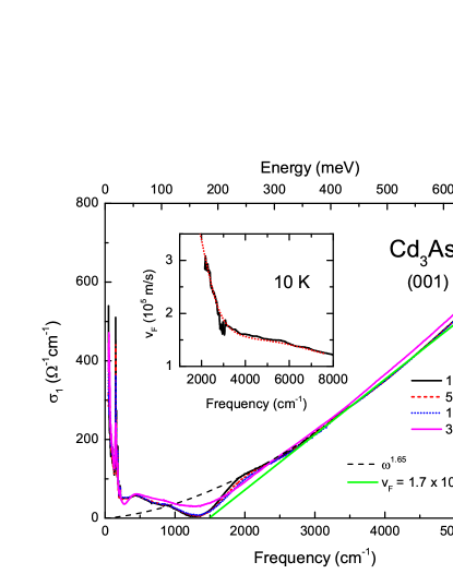
The first striking result of our investigation is a power-law behavior of between approximately 2000 and 8000 cm-1: with . This power-law conductivity is basically independent on temperature.

The straightforward application of Eq. (1) yields , i.e., a sublinear dispersion, , of the Dirac bands in Cd3As2. This dispersion is valid only for the energies above 250 meV ( 2000 cm-1), as the observed power law in does not extend below this frequency. Also, Eq. (1) does not take into account the asymmetry between the valence and conduction bands, which is present in Cd3As2 Liu2014Nat ; Jeon2014 . Hence, the obtained dispersion is basically an effective approximation. Nevertheless, the sublinear dispersion at high energies is in qualitative agreement with the dispersion derived from Landau-level spectroscopy Jeon2014 , with ARPES results Neupane2014 , as well as with band-structure calculations Borisenko2014 ; Jeon2014 . One could imagine that the Dirac bands in Cd3As2 get more narrow when the Dirac point is approached as depicted by the sketch in Fig. 2. Eventually, the bands become linear, but we cannot probe the linear dispersion by optical-conductivity measurements, because, as will be discussed below, the Fermi level in our sample is shifted with respect to the Dirac point.
The dielectric constant (bottom panel of Fig. 2) is negative at low frequencies and crosses zero at 400 cm-1. The crossing point is independent on temperature and is set by the screened plasma frequency of the free carriers, . Very similar values of have been reported previously Gelten1980 ; GeltenPhD ; Houde1986 indicating similar carrier concentrations in naturally grown samples. At higher frequencies takes a positive sign, reaching values up to 17 at 1500 – 2000 cm-1.
IV Discussion
In the simplest case of symmetric 3D Dirac cones, the slope of the linear due to interband contributions is directly related to the (isotropic) Fermi velocity of Dirac fermions Hosur2012 ; Bacsi2013 ; Timusk2013 :
| (2) |
where is the number of nondegenerate cones and all Dirac points are considered to be at the Fermi level. If the Fermi level is not at the Dirac point (), Eq. (2) is replaced by Ashby2014 :
| (3) |
where is the Heaviside step function and any carrier scattering is ignored.
In Fig. 3 we re-plot on a double-linear scale as relevant for further considerations. From Figs. 2 and 3 one can see that the low-temperature almost vanishes ( cm-1) at around 1300 cm-1 (160 meV). The power-law conductivity starts at 2000 cm-1 (250 meV). Following Ref. Ashby2014, and Eq. (3), we associate this steplike feature in with the position of the Fermi level.
The power-law conductivity discussed above can be roughly approximated by a straight line (the best fit is achieved between 3000 and 4500 cm-1). By setting (two spin-degenerate cones) in Eq. (2), we obtain m/s. Alternatively, one can estimate from the derivative of the interband conductivity, i.e. from () at cm-1:
| (4) |
as it is shown in the inset of Fig. 3. As it can be seen from the figure, the typical values of ( to m/s) are somewhat smaller than the published results, which range from m/s to m/s Borisenko2014 ; Liu2014Nat ; Neupane2014 ; Liang2015 ; Jeon2014 ; Cao2015 ; He2014 . Note however, that we have evaluated an energy-dependent Fermi velocity: strongly increases as is reduced. In other words, might actually meet the literature values when approaching the Dirac points. The rise of at is exactly the behavior expected for narrowing Dirac bands.

In order to get a more quantitative description of the optical conductivity in Cd3As2, one needs to implement a model. So far, there is no accurate model for the optical conductivity of a 3D doped Dirac semimetal with sublinear band dispersion. Building such a model goes beyond the present work Lifshitz . Below, we will use a simple model of linear spectrum with the purpose of extracting the Fermi-level position and explaining its broadening. This model will also effectively describe the leveling off the interband conductivity spectrum at low frequencies.
The model is based on considering self-energy effects in the spirit of Ref. Benfatto2008, and is given in the Supplemental Material. The real parts of the conduction and valence-band self energies are approximated by the constant Re and Re, respectively. We hence obtain for the interband conductivity
| (5) |
where Morimoto . The conduction-band energies have been pushed up by , while the valence-band energies are lowered by the same amount. Alternatively, Eq. (5) is the interband conductivity of a simple band structure with , which could be thought of as a first rough approximation to the case of the Dirac cones that get narrow as energy approaches the Dirac point. The Fermi energy is measured from the Dirac point without self-energy corrections included, and so must be larger than for finite doping away from charge neutrality. If impurity scattering cannot be neglected, the Heaviside function can be replaced by
| (6) |
where represents a frequency-independent impurity scattering rate.
A combination of Eqs. (5) and (6) is now employed to model the experimental data; the best fit is plotted in Fig. 4. Note, that this model does not include the intraband conductivity. The best description of the experimental curve was achieved with cm-1 ( meV), cm-1, cm-1, and m/s. The value of , which is found to be smaller than the Fermi energy, has to be considered as a fit parameter only. The fit is not perfect, as the model doesn’t include the deviations from the band linearity discussed above. Nevertheless, the model grasps the main features of the interband conductivity in Cd3As2.
The obtained position of the Fermi level (100 meV) seems to be quite reasonable for our sample, taking into account its carrier concentration ( cm-3) and keeping in mind that meV was reported for a sample with cm-3 Jeon2014 and meV for cm-3 Cao2015 .
Although the scope of this work is the interband conductivity in Cd3As2, let us briefly discuss the experimental results at the lowest frequencies measured. The intraband conductivity is represented by a narrow Drude component (best seen in Fig. 5) and an absorption band of peculiar shape at cm-1 (see Figs. 3 and 4). The nature of the band might be related to localization and/or correlation effects. In any case, the presence of this band makes it impossible to fit the intraband conductivity for cm-1 with a simple free-electron Drude term. One can see, however, that the narrow Drude peak is getting somewhat narrower as due to a modest decrease of scattering. Let us note that the spectral weight related to the low-frequency absorbtion of delocalized carriers remains temperature independent because the screened plasma frequency, discussed above in connection to the dielectric constant, is independent of temperature.
In addition to electronic contributions, the low-frequency conductivity renders a large number of phonon modes marked by arrows in Fig. 5. We can distinguish 14 infrared-active phonon modes in the frequencies between approximately 100 and 250 cm-1. As the temperature is reduced, the phonons become sharper. More details on the low-frequency conductivity in Cd3As2 will be given in a separate paper.

V Conclusions
We found the dc resistivity and the optical conductivity of [001]-oriented -doped ( cm-3) Cd3As2 to be isotropic within the (001) plane. The real part of the frequency-dependent conductivity follows a power law, , in a broad frequency range, 2000 to 8000 cm-1. We interpret this behavior as the manifestation of interband transitions between two Dirac bands with a sublinear dispersion relation, . The Fermi velocity falls in the range between and m/s, depending on the distance from the Dirac points.
At 1300 cm-1 (160 meV), we found a diminishing conductivity, consistent with observations of an “optical gap”, made in the 1960s Turner1961 . However, we hesitate to follow the traditional interpretation of this feature and to straightforwardly relate it to a gap in the density of states. Applying recent models for the optical response of Dirac/Weyl semimetals, we instead relate this feature to the Fermi level, which is positioned around meV above the Dirac points, and which is consistent with the carrier concentration.
VI Acknowledgements
Acknowledgements.
Ruud Hendrikx at the Department of Materials Science and Engineering of the Delft University of Technology is acknowledged for the x-ray analysis. We are grateful to Gabriele Untereiner for sample preparation and other technical assistance. Sample-characterization work of Hadj M. Bania is highly appreciated. We thank Hongbin Zhang, Sergueï Tchoumakov, Marcello Civelli, Robert Triebl, and Gernot Kraberger for their efforts in calculations of the Cd3As2 optical conductivity, for sharing their results with us, and for many useful conversations. A. A. N. is grateful to Prof. Ernest Arushanov for his interest in this work and useful discussions. This work was supported by the Deutsche Forschungsgemeinschaft (DFG).VII Supplemental material
VII.1 Sample growth
Single crystals of Cd3As2 have been grown by vapor transport from material previously synthesized in argon flow with the flow rate of a few cm3/min Nateprov2015 . The temperatures in the evaporation and growth zones are 520 ∘C and 480 ∘C, respectively. By subsequent annealing at room temperature the electron mobility is enhanced while at the same time the electron concentration decreases Rambo1979 . Well-defined crystals with facets measured a few millimeters in each direction are harvested after 24 hours of the growth process.
The lattice parameters have been obtained by x-ray diffraction: nm and nm, in good agrement with recent measurements reporting a tetragonal unit cell with only light deviations from a cubic structure Ali2014 .
VII.2 Kramers-Kronig analysis
For Kramers-Kronig analysis, extrapolations to zero frequency have been made using the Hagen-Rubens relation in accordance with the temperature-dependent dc resistivity measurements (Fig. 5 of the article). For the temperature-independent extrapolation to , we utilized published reflectivity data, obtained in ultra-high vacuum for up to 170 000 cm-1 (21 eV) Zivitz , applying the procedure proposed by Tanner Tanner2015 , which utilizes x-ray atomic scattering functions for calculating the optical response for frequencies from 21 to 30 000 eV and the free-electron extrapolation for frequencies above 30 keV.
In order to check the robustness of our Kramers-Kronig analysis, we replaced the reflectivity data of Ref. [Zivitz, ] by three other data sets available in the literature for the frequency range from approximately 1 to 5 eV. Namely, we used: (i) the polycrystalline data from Ref. [Karnicka, ]; (ii) the single-crystal data from the same reference; and (iii) the most recent single-crystal data from Kozlov et al. Kozlov . All these data sets, as well as the data of Ref. [Zivitz, ], show rather similar overall reflectivity with two strong peaks at approximately 1.8 and 4 eV; the peak at 1.8 eV shows up in our data as well. We have found that at frequencies below 1.2 eV (10 000 cm-1) all these different extrapolations affect the outcome of the Kramers-Kronig analysis only marginally. However, it is essential not to neglect the strong peak in reflection at around 4 eV. If we ignore the 4-eV peak in our Kramers-Kronig analysis and use instead the free-electron () extrapolation right from the highest data point, the exponent of the power-law dependence of the optical conductivity between 2000 and 8000 cm-1, discussed in the article, will be reduced from 1.65 to 1.2.
VII.3 Interband optical conductivity of linearly dispersed bands with self-energy effects
For a Dirac/Weyl semimetal in the pure limit with no impurity scattering, the dynamic longitudinal optical conductivity associated with a single Weyl point can be expressed as Ashby2014 :
| (7) |
(we adopt for calculations here). In the presence of self-energy effects, the -functions in Eq. (7) are to be replaced by the corresponding conduction () and valence () band spectral functions:
| (8) |
For our purposes, it will be sufficient to take the imaginary part of the self energy to be infinitesimal small and the real part of the self energy to be some constant with , so that the conduction band is translated up by and the valence band down by . The real part of the conductivity then takes the form:
| (9) |
which works out to be
| (10) |
Note, that is the optical gap and is zero for all photon energies below when . If the system is doped (), then the lower cut-off in the conductivity is rather than .
References
- (1) T. O. Wehling, A. M. Black-Schaffer, and A. V. Balatsky, Adv. Phys. 63, 1 (2014).
- (2) P. Hosur, S. A. Parameswaran, and A. Vishwanath, Phys. Rev. Lett. 108, 046602 (2012).
- (3) A. Bácsi and A. Virosztek, Phys. Rev. B 87, 125425 (2013).
- (4) The linear () is to be present in the 3D Dirac systems regardless the origin of the Dirac point(s). For example, a linear in frequency conductivity was observed in the topologically trivial inverted-band semiconductor Hg1-xCdxTe with by M. Orlita et al., Nat. Phys. 10, 233 (2014).
- (5) T. Timusk, J. P. Carbotte, C. C. Homes, D. N. Basov, and S. G. Sharapov, Phys. Rev. B 87, 235121 (2013).
- (6) R. Y. Chen, S. J. Zhang, J. A. Schneeloch, C. Zhang, Q. Li, G. D. Gu, and N. L. Wang, Phys. Rev. B 92, 075107 (2015).
- (7) Q. Li, D. E. Kharzeev, C. Zhang, Y. Huang, I. Pletikosic, A. V. Fedorov, R. D. Zhong, J. A. Schneeloch, G. D. Gu, and T. Valla, arXiv:1412.6543.
- (8) Z. Wang, H. Weng, Q. Wu, X. Dai, and Z. Fang, Phys. Rev. B 88, 125427 (2013).
- (9) S. Borisenko, Q. Gibson, D. Evtushinsky, V. Zabolotnyy, B. Büchner, and R. J. Cava, Phys. Rev. Lett. 113, 027603 (2014).
- (10) Z. K. Liu, J. Jiang, B. Zhou, Z. J.Wang, Y. Zhang, H. M.Weng, D. Prabhakaran, S.-K. Mo, H. Peng, P. Dudin, T. Kim, M. Hoesch, Z. Fang, X. Dai, Z. X. Shen, D. L. Feng, Z. Hussain and Y. L. Chen, Nature Mater. 13, 677 (2014).
- (11) M. Neupane, S.-Y. Xu, R. Sankar, N. Alidoust, G. Bian, C. Liu, I. Belopolski, T.-R. Chang, H.-T. Jeng, H. Lin, A. Bansil, F. Chou, and M. Z. Hasan, Nature Commun. 5, 3786 (2014).
- (12) S. Jeon, B. B. Zhou, A. Gyenis, B. E. Feldman, I. Kimchi, A. C. Potter, Q. D. Gibson, R. J. Cava, A. Vishwanath, and A. Yazdani, Nature Mater. 13, 851 (2014).
- (13) L. P. He, X. C. Hong, J. K. Dong, J. Pan, Z. Zhang, J. Zhang, and S. Y. Li, Phys. Rev. Lett. 113, 246402 (2014).
- (14) T. Liang, Q. Gibson, M. N. Ali, M. Liu, R. J. Cava, and N. P. Ong, Nature Mater. 14, 280 (2015).
- (15) M. N. Ali, Q. Gibson, S. Jeon, B. B. Zhou, A. Yazdani, and R. J. Cava, Inorg. Chem. 53, 4062 (2014).
- (16) W. J. Turner, A. S. Fischler, and W. E. Reese, Phys. Rev. 121, 759 (1961).
- (17) M. Iwami, M. Yoshida, and K. Kawabe, Jpn. J. Appl. Phys. 12, 1276 (1973).
- (18) M. J. Gelten, C. M. van Es, F. A. P. Blom, and J. W. F. Jongeneelen, Solid State Commun. 33, 833 (1980).
- (19) M. J. Gelten, Optical properties of cadmium phosphide and cadmium arsenide, Doctor in de Technische Wetenschappen Thesis, Technische Hogeschool, Eindhoven, 1985.
- (20) O. Houde, S. Jandl, M. Banville, and M. Aubin, Solid State Commun. 57 247 (1986).
- (21) Cadmium arsenide (Cd3As2) optical properties, dielectric constants, in Non-Tetrahedrally Bonded Elements and Binary Compounds I, Landolt-Börnstein – Group III Condensed Matter, Vol. 41C (Springer, Berlin, 1998) and references therein.
- (22) V. V. Sobolev and N. N. Syrbu, Izv. Akad. Nauk SSSR, Neorg. Mater. 2, 1011 (1966).
- (23) V. V. Sobolev, N. N. Syrbu, T. A. Zyubina, and Y. A. Ugai, Fiz. Tekh. Poluprovodn. 5, 327 (1971) [Sov. Phys. Semicond. 5, 279 (1971)].
- (24) M. Zivitz and J. R. Stevenson, Phys. Rev. B 10, 2457 (1974).
- (25) K. Karnicka-Moscicka, A. Kisiel, and L. Zdanowicz, Solid State Commun. 44, 373 (1982).
- (26) A. I. Kozlov, V. V. Sobolev, and A. F. Knjazev, Semiconductors 39, 285 (2005).
- (27) C. P. Weber, E. Arushanov, B. S. Berggren, T. Hosseini, N. Kouklin and A. Nateprov, Appl. Phys. Lett. 106, 231904 (2015).
- (28) C. C. Homes, M. Reedyk, D. A. Cradles, and T. Timusk, Appl. Opt. 32, 2976 (1993).
- (29) P. E. C. Ashby and J. P. Carbotte, Phys. Rev. B 89, 245121 (2014).
- (30) J. Cao, S. Liang, C. Zhang, Y. Liu, J. Huang, Z. Jin, Z.-G. Chen, Z. Wang, Q. Wang, J. Zhao, S. Li, X. Dai, J. Zou, Z. Xia, L. Li F. Xiu, Nature Commun. 6, 7779 (2015).
- (31) The electron-hole asymmetry of the Dirac bands as well as the influence of the Lifshitz-transition points, which exact position is debatable, have to be taken into account in a complete optical-conductivity model for Cd3As2.
- (32) L. Benfatto and E. Cappelluti, Phys. Rev. B 78, 115434 (2008).
- (33) For , Eq. (5) is reduced to the form proposed for the optical conductivity in so-called Weyl-Mott insulators by T. Morimoto and N. Nagaosa, Sci. Rep. 6, 19853 (2016).
- (34) A. Rambo and M. J. Aubin, Can. J. Phys. 57, 2093 (1979).
- (35) D. B. Tanner, Phys. Rev. B 91, 035123 (2015).