Accidental degeneracy and topological phase transitions in two-dimensional core-shell dielectric photonic crystals
Abstract
A simple core-shell two-dimensional photonic crystal is studied where the triangle lattice symmetry and the point group symmetry give rich physics in accidental touching points of photonic bands. We systematically evaluate different types of accidental nodal points at for transverse-magnetic harmonic modes when the geometry and permittivity of the core-shell material are continuously tuned. The accidental nodal points can have different dispersions and topological properties (i.e., Berry phase). These accidental nodal points can be the critical states lying between a topological phase and a normal phase of the photonic crystal. They are thus very important for the study of topological photonic states. We show that, without breaking time-reversal symmetry, by tuning the geometry of the core-shell material, a phase transition into the photonic quantum spin Hall insulator can be achieved. Here the “spin” is defined as the orbital angular momentum of a photon. We study the topological phase transition as well as the properties of the edge and bulk states and their application potentials in optics.
pacs:
42.70.Qs,78.67.Pt,03.65.VfI Introduction
The Ginzburg-Landau paradigmGL gained wide success in describing phase transitions before the discovery of the quantum Hall effectqhe ; fqhe . The emergence of topological states of matter raises new challenges in understanding the states of matter and phase transitions. Topological states of matter offer new physics and applications in electronic systems such as topological insulators and topological semimetals (e.g., graphenegraphene ). The conical dispersions in topological semimetal and the helical edge states of topological insulators are found to be useful for a lot of applicationsTIreview . Since Haldane and Raghu’s seminal work which brought the quantum anomalous Hall effect to the realm of photonicsRaghu , more and more researches are focused on the topological effects in photonic crystals (PhCs)phTI .
PhCs are periodically arranged dielectric materials which break the continuous translation symmetry that gives the dispersion of light in homogeneous materials. The resulting photonic spectrum is the photonic energy bands similar to the electronic energy bands in solid crystalseli ; sajeev . The emergence of photonic energy bands and band gaps introduces tremendous advantages in manipulating lightbook . Unlike previous studies on trapping light with photonic band gaps, in this work we focus on the nodal points in photonic bands in two-dimensional (2D) triangle PhCs. We examine their relationships with Dirac (and Dirac-like) points and topological phase transitions. Nontrivial Berry phases assign a topological winding number to the nodal points, making them mother states of quantum spin Hall insulators and quantum anomalous Hall insulators (denoted as the and topological insulators, respectively)TIreview ; qahe . The topological nodal points studied here are induced by accidental degeneracy’s instead of deterministic degeneracy’s due to, e.g., nonsymmorphic or sublattice symmetry (e.g., in photonic grapheneph-gra ). Accidental degeneracy in 2D PhCs have attracted a lot of research attention in recent years. In square lattice photonic crystals, a conical Dirac-like dispersionct2d was found theoretically. At the Dirac point the photonic crystal can be regarded as a lossless effective medium of zero refractive indexct2d ; Sakoda .
Photonic analog of time-reversal symmetric topological insulators using bi-anisotropic metamaterials was proposedz2-ph , where the coupling between the electric field and magnetic field plays the same role as the spin-orbit coupling in electronic topological insulators. Recently, the topological phase transition between normal photonic band gap materials and a photonic topological insulator was proposed in 2D PhCs using normal dielectric materials with isotropic permittivityhuxiao . The 2D PhCs that realize such a transition is a triangle lattice where there are six cylinders in each unit cell forming a pattern with symmetry. By tuning the position of the cylinders a photonic band gap carrying topology can be formed. At the boundary between the topological phase and the trivial phase, a double Dirac cone is formed precisely at the geometry that the lattice becomes a honeycombhuxiao . Therefore, the double Dirac cone is induced by a deterministic degeneracy due to the sublattice symmetry of the honeycomb lattice. Recently Dirac-cones are studied in PhCsSakoda ; pgs and phononic crystalsmei .
In this work, we propose a simpler realization of the photonic analog of the topological insulator, using core-shell dielectric materials. There is only a single core-shell cylinder at the center of each unit cell. The core-shell structure has continuous rotation symmetry which is compatible with the largest point group symmetry of the triangle lattice. This provides the condition for the realization of the topological phase. Moreover, it off the possibilities to achieve various degeneracy’s such as Dirac-like cone, double Dirac cone, and quadratic band touching. We systematically calculate the accidental degeneracy’s at the Brillouin zone center and the topological phase transitions in the 2D core-shell dielectric PhCs. The core-shell triangle photonic crystal structure is simple and mechanically stable and hence it is compatible with colloidalcolloid self-assembled structure as well as biological systemsbio . Our study shows how topological phases of photons can be realized in simple 2D dielectric PhCs and various phases can be induced by tuning the geometry of the dielectric materials.
II 2D TRIANGLE PHOTONIC CRYSTALS
Among common 2D PhCs, triangle photonic crystals have the largest point group symmetrypgs . As will be shown below the 2D triangle PhCs can host several kinds of topological nodal points. These nodal points are the mother states of different types of photonic topological insulators. In the triangle lattice, the point has two kinds of 2D irreducible representations in the symmetry, which are denoted as the and representations, respectivelysa-book . The associated Bloch waves are referred as the and modes, respectively. Each representation has two Bloch waves, which can be reorganized into a pair of modes connected by time-reversal operation. Here the relevant modes are the and modes, which are denoted as (pseudo-) spin up and spin down states of the bands. Similarly, the and modes are denoted as the (pseudo-) spin up and spin down states for the bands.
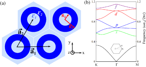
The 2D core-shell dielectric structure in triangle lattice is shown in Fig. 1(a). Its outer and inner radii are denoted as and , respectively. The dielectric constant of the core-shell material and the background material are and , respectively. The lattice constant is set as . We define the inverse structure by the exchange of and . The inverse structure is hence a core-shell air cylinder in dielectric background. Our architecture is one of the simplest 2D PhCs that can support rich physics of topological nodal points and topological phase transitions.
By numerically solving the Maxwell’s equations for transverse magnetic (TM) harmonic modes, of which the electric field is along the core-shell cylinder (i.e., the direction). Fig. 1(b) shows a typical band structure of the PhC. The band structure is calculated by COMSOL based on the finite-element method. In this band structure, the eigen-modes at the point exhibit orbital symmetry of the and waves from low frequency to high frequency. These modes correspond to the , , and modes of the point group symmetrysa-book . The labeling of bands with , , and modes is only effective at the point which possesses the symmetry. Away from the point these modes mix with each other and their order in frequency may change. Nevertheless, the labels clearly reveal the accidental band degeneracy and band inversion at the point. Besides, the and modes carry physical meanings. The photonic bands can be viewed as derived from transfer (hopping) of local Mie resonances of the core-shell structures between adjacent unit cells. Such a tight-binding understanding of the photonic bands has successfully connected the photonic bands with the Mie resonances of and symmetriestb ; kivshar . Thus the Mie resonances can be regarded as the “atomic orbits” for photonic energy bands, as it plays the same role as the atomic orbits in electronic energy bands.
The and ( and ) modes are singlet states, while the and modes are doubly degenerate, according to the symmetry. By continuously changing the radii and or the dielectric constant, different bands cross each other, leading to accidental degeneracy’s at the point. The accidental degeneracy usually results in linear or quadratic dispersion. The scale invariance of the Maxwell’s equations dictates that the independent variables in our system are the inner and outer radii (divided by the lattice constant) as well as the ratio of the two dielectric constants . The properties of the photonic bands for are well-studied in the literature, where no topological nodal point or topological band structure is found.
III PHASE DIAGRAM
We first discuss the eigen-frequency of the and bands at the point. We use the following dimensionless quantity to characterize the relative - band-gap size at the point,
| (1) |
where and are the egien-frequency’s of the and modes at the point, respectively.
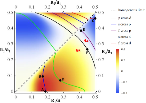
By numerically calculating the photonic band structure, we obtain in the - parameter space with and (see Fig. 2). The figure clearly demonstrates the - band inversion which can result in photonic analog of the topological insulator. The properties of this photonic topological states will be discussed in details below. We incorporate in the upper triangle of Fig. 2 the phase diagram for the reversed structure, where the core-shell cylinder of air induces the photonic energy bands. The diagonal line is the homogeneous limit, which can be regarded as no dielectric or no air (for the inverse structure). The influence of on the phase diagram will be discussed below.
The color scheme represents: the red region has bands lower (in frequency) than the bands at the point, while the blue region has bands higher than the bands at the point (i.e., - band inversion). The blue region thus represents the topological phase (), while the red region represents the normal phase (topologically trivial, ). The parity inversion at the point for the - reversed photonic bands dictate the topologyfuprb . At the boundary between the topological phase and the normal phase, the double Dirac-cone dispersion emerges at the point. The properties of the photonic topological insulator will be discussed in details below.
In addition, we use the blue (red) curve in Fig. 2 to denote the crossing between the and bands (the and bands) in the phase diagram. These two situations lead to Dirac-like cones at the point. The crossing between the and bands (the and bands) are denoted as the green and purple curves in the phase diagram. These crossings lead to quadratic band touching at the point. All these accidental band degeneracy’s and the properties of the nodal point will be discussed in details below.
Other important information revealed by Fig. 2 is the geometric conditions for the emergence of various nodal points in the photonic spectrum. These nodal points are important in several reasons. First, they are the mother states of topologically nontrivial states of photons. An example has been demonstrated above for the relation between the double Dirac cone and the photonic topological insulator. The Berry phase of each band is closely related to the formation of the photonic topological states. Usually, topological nodal points are the critical states between normal band gaps and topological insulators. By introducing time/parity breaking perturbations, the double-Dirac-cone state can become a photonic quantum anomalous Hall insulator ( topological insulator) or a topological insulator, or a trivial photonic band gap material, depending on the specific gap opening perturbationsonoda . Our study includes the triangle photonic crystals with dielectric rods as a special limit of =0. From the phase diagram, it is clear that the - band inversion cannot be attained using dielectric rods with =0. Thus the dielectric rod photonic crystals cannot support double Dirac cone. They can only support Dirac-like cone due to - degeneracy or quadratic band touching due to - degeneracy. For the inverse structure a simple air cylinder can only support - degeneracy.
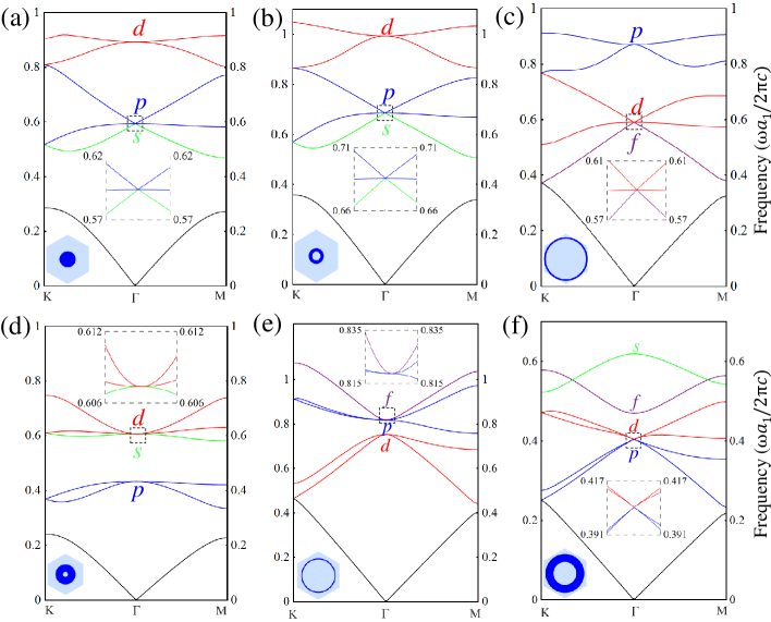
We plot in Fig. 3 the band structures of different kinds of accidental degeneracy’s marked by the black points in Fig. 2. In Figs. 3(a) and 3(b), the linear dispersion due to the accidental degeneracy of the singlet mode and the doubly degenerate modes are plotted, leading to the Dirac-like cone. The Dirac-like cone is associated with a cone and a flat band intersecting at the Dirac point. Its effective Hamiltonian is where is the pseudo-spin 1 consisting of three modes , , and ct2d . is the group velocity around the Dirac point. The upper, lower and flat bands have pseudo-spin along the wave vector direction as 1, -1, and 0, respectively.
The Dirac-like cone can emerge in photonic crystals with (cylinder rods) as well as for finite (hollow cylinders). The photonic dispersions for these two situations are illustrated in Figs. 3(a) and 3(b), respectively. Another Dirac-like cone dispersion is shown in Fig. 3(c) due to accidental degeneracy of the singlet mode and the doubly degenerate modes. Linear, conical dispersion appears for the - and - degeneracy’s because the parity of the and ( and ) modes are different. According to the theorymei2 ; mei3 , the linear in coupling between two photonic bands originates from the matrix element which is finite only between bands with different parities. For bands with the same parity, such coupling is quadraticmei2 ; mei3 . The quadratic dispersion around the touching point of the and bands is shown in Fig. 3(d), while the quadratic band touching around the - degeneracy is shown in Fig. 3(e).
The accidental degeneracy of the doublets and the doublets [Fig. 3(f)] carries nontrivial topological properties which are the main focus of this work. Since the parity of the modes and the modes are different, the dispersion around the accidental degeneracy is conical. The two fold degeneracy’s of the and bands result in a double Dirac cone that resembles the dispersion of Dirac’s famous equation for electron and positron with vanishing mass in 2D systems.
We now exploit the theory to derive the effective Hamiltonian for the photonic bands near the nodal points. The Maxwell’s equation for the TM modes can be written as
| (2) |
where is the band index and is the Bloch function of the magnetic field of photon. The Bloch function is normalized as with denoting the unit cell (i.e., integration in a unit cell). The Hermitian operator can be viewed as the photonic Hamiltonian. Expanding the Bloch function in the basis of the Bloch wavefunctions at the point, , one can establish a Hamiltonian,
| (3) |
where is the eigen-frequency of the band at the point. The matrix element of is given by
| (4) |
We notice that the matrix element of is nonzero only when the and bands are of different parity. Using the above theory, to the linear order in , the effective Hamiltonian of the and bands is written in the basis of as,
| (5) |
where , and is the coupling coefficient. The double Dirac-cone appears at the situations with - degeneracy, . The group velocity for the double Dirac-cone dispersion at point is then (positive group velocity for bands above the Dirac point, negative group velocity for bands below). The bands behave as the valence band and the bands behave as the conduction band in our photonic crystals. Note that the coupling between the and bands are within the same pseudo-spin, i.e., between and , or between and . The Berry phase for a loop circulating the Dirac point is for spin up/down bands above the Dirac point. The total Berry phase is zero, in accordance with time-reversal symmetry.
The physics described by Eq. (5) resembles that of the quantum spin Hall effect in electronic systems. The - inversion at the point leads to the formation of photonic topological insulators which have helical edge states. The phase transition from normal photonic band gaps with trivial topology to the photonic topological insulator takes place at the black line in Fig. 2, where the double Dirac cone emerges. The key information in Fig. 2 is the appearance of two regions support photonic topological insulators (the two blue regions). This takes place for hollow dielectric cylinders with large outer and inner radii, or for hollow air cylinders with small inner radius. We remark that although the - band gap of the topological insulator can be quite large at the point, , for both normal and reversed structures, the complete photonic band gap is reduced, particularly for the inverse structure. The photonic topological insulators have helical edge states which can enable unprecedented manipulation of light flow. For example, light propagation can be controlled by the orbital angular momentum. We shall discuss the properties of the edge states below.
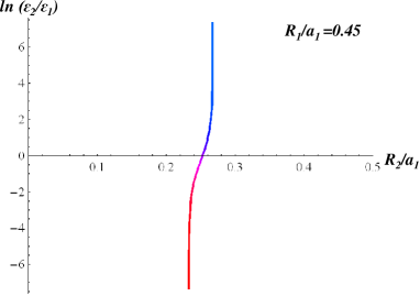
It is natural to ask how the phase diagram changes when the permittivity ratio is tuned. In most photonic crystals the photonic band gap increases with the permittivity ratio book . Here we find that, quite interestingly, the phase boundary between the topological insulator and the normal photonic band gap changes negligibly for a very broad range of the permittivity ratio. This interesting property is demonstrated in Fig. 4 where we examine the phase boundary along the axis for different permittivity ratio for fixed outer radius . The critical value of where the double Dirac cone emerges is insensitive to the permittivity ratio in a very wide range. Although the calculation is done for , the observed behavior holds true for other values of the outer radius . In fact, we have chosen the in the calculation such that the dependence of the critical value of on the permittivity ratio is the strongest. The regions with negative value of in Fig. 4 stands for the inverse structure photonic crystal. The horizontal axis represents the case with , i.e., the homogenous limit. In the homogeneous limit the photonic band gaps vanish and all the photonic bands become plane waves. Thus they cannot be associated with the and symmetries. The homogeneous limit is a singular limit for the discussion the topological nodal points and - inversion. This explains the discontinuity of, e.g., the - band crossing curve for the normal and inverse structure in the phase diagram upon crossing the homogeneous limit. Nonetheless, the - band crossing seems to undergo a “continuous transition” from the normal structure to the inverse structure. The possible physical scenario in approaching the homogeneous limit is that the plane-wave component continuously increase to 100%, while the wave (the local Mie resonances of the hollow cylinder) components gradually vanish in approaching the homogeneous limit.
IV EDGE STATES OF THE TOPOLOGICAL INSULATORS
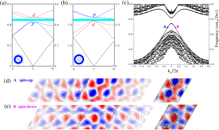
We now discuss the properties of the edge states of the photonic topological insulators. First, let us consider the and points in Fig.2. The point has normal band structure, while the point is a photonic topological insulator. There is a common complete band gap marked by the cyan region in Figs. 5(a) and 5(b). When these two photonic crystals are put together, there is topology induced edge states. The topology is protected by the pseudo-time-reversal symmetry. The pseudo-time-reversal operation is with (the complex conjugation operator) being the genuine time-reversal operator. Here is an operator acting on the pseudo-spin space for both the and bands which can be written as a combination of the symmetry operations (see Ref. huxiao, ) to ensure that . The latter is crucial in mimicking electronic topological insulator in photonic crystals. The pseudo-spin matrices transform as follows, under pseudo-time-reversal operation, for . Under the genuine time-reversal operation, , , and , because and (since and for bands, while and for the bands).
The symmetry breaks down at the boundary between the two photonic crystals. Hence the boundary introduces perturbations that gap the helical edge states. The size of the gap depends on the strength of the perturbation. However, since the bulk topology of the two photonic crystals is distinct, there is topology guaranteed edge states, although they may not be gapless. This is the essential feature for bosonic analog of the topological insulators. A typical calculation of the edge states is presented in Fig.5(c). The helical edge states are gapped at . Away from the point the helical feature of the edge states is clearly demonstrated in Figs.5(d) and 5(e). The edge states at the point is mostly spin-down (due to the perturbation that gaps the point, the point mix slightly with spin-up) as recognized from the real space distribution of the Poynting vector. Similarly the point is mostly spin up and it has positive group velocity, while the point has negative group velocity. Hence the helical character of the edge states is preserved except near the point.
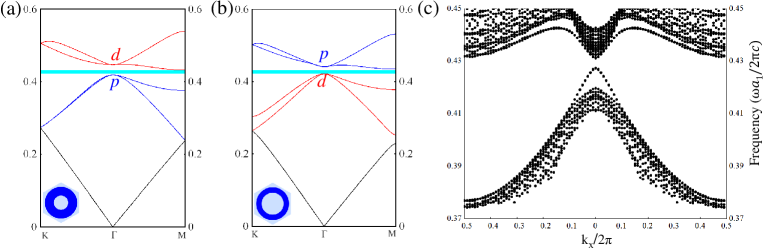
In some situations the two photonic crystals do not share a common photonic band gap. We can slightly change the or of the structure to get the common photonic band gap. Since the - inversion depends negligibly on the ratio of the two permittivity, this does not change the topological properties of the photonic crystals. For example, if the photonic crystal with normal band structure has =0.45, =0.2, =9, and =1 [see in Fig. 6(a)], while the photonic crystal with nontrivial topology has =0.45, =0.3, =12, and =1 [see in Fig. 6(b)]. The two photonic crystals have a common band gap marked by the cyan ribbon. When those two photonic crystals are put together the topology induced edge states are found [see in Fig. 6(c)].
From symmetry considerations, the boundaries break the pseudo-time-reversal symmetry but still keeps the (genuine) time-reversal symmetry. The spin-operators that are even under time-reversal operation are the and . Thus there can be two types of “mass terms” that gap the edge states. The general form of the edge Hamiltonian that obeys the time-reversal symmetry is where is the group velocity, and are two real quantities. The magnitude of the two masses, and , depend on the specific geometry of the boundary. The energy gap at is . Finally, we remark that if and are position-dependent, they can induce additional Berry-phase that modulates photon propagation along the boundary.
V APPLICATION POTENTIALS
The effective refractive index of the photonic crystal can be positive or negative, depending on the frequency of the light. By matching the frequency and wave vector parallel to the boundary, we find, in agreement with Ref. refrac, , that the effective refractive index is frequency dependent,
| (6) |
where and are the angle of incidence and refraction, respectively. is the frequency of the Dirac point. The above equation demonstrates that the effective refractive index can be tuned via the frequency. Both positive and negative refractive indices can be achieved, as indicated in Fig. 7. We emphasize that the effective refractive index here are in the range range , which are unattainable for natural (lossless) materials. Therefore, the photonic crystal with double Dirac cone can serve as a particular type of lossless metamaterial with unprecedented ability of manipulating light.
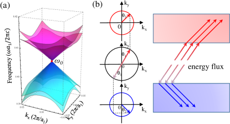
The edge states can be viewed as unconventional waveguides that correlates the direction of light flow and its group velocity with the angular momentum of light (as demonstrated in Fig.5). In addition, when the frequency of the light is in the bulk photonic bands, the propagation of light are influenced by the Berry phase in the bulk bands due to the pseudo-spin-orbit coupling, which leads to the spin Hall effect of lightberry ; onoda2 . The spin-dependent Berry phase can lead to anomalous velocity and shift in a scattering/reflection set-uponoda2 . Due to the time-reversal symmetry, these anomalous velocity and shift are opposite for opposite pseudo-spins. These properties can be exploited as angular-momentum selective transmission and filtering for advanced photonic circuits.
VI CONCLUSION AND DISCUSSIONS
Using a simple architecture of core-shell triangle photonic crystal with point group symmetry we have systematically studied the evolution of the nodal points in photonic energy bands for various geometry and (isotropic) permittivity parameters. We show that such a simple photonic crystal can support photonic topological insulators. Compared with previous proposal of photonic topological insulators, our architecture is much simpler and hence feasible for fabrications and experiments. The edge states of the topological insulators, unlike for electronic systems, are not ensured to be gapless. Nevertheless, they show properties similar to the helical edge states in electronic systems, such as spin-dependent propagation directions. We also give a full phase diagram for the topological nodal points, Dirac-like cones and double Dirac cones, for various geometric parameters. These topological nodal points are proximate to topologically nontrivial photonic band gaps. The physical origin of the topological nodal points as well as their properties such as Berry phase, (pseudo-)spin-orbit coupling are revealed. Dirac cones at can be exploited to tune the effective refractive index to the range which are unattainable in natural (lossless) materials. These properties, together with the Berry phases of photon, offer great potential for future advanced photonics.
Acknowledgements
We thank supports from the National Science Foundation of China for Excellent Young Scientists (grant no. 61322504). J.H.J acknowledges supports from the faculty start-up funding of Soochow University. He also thanks Sajeev John, Xiao Hu, and Zhi Hong Hang for helpful discussions.
References
- (1) V.L. Ginzburg and L.D. Landau, Zh. Eksp. Teor. Fiz. 20, 1064 (1950).
- (2) K. v. Klitzing, G. Dorda, and M. Pepper, Phys. Rev. Lett. 45, 494 (1980).
- (3) D. C. Tsui, H. L. Stormer, and A. C. Gossard, Phys. Rev. Lett. 48, 1559 (1982).
- (4) A. H. Castro Neto, F. Guinea, N. M. R. Peres, K. S. Novoselov, and A. K. Geim, Rev. Mod. Phys. 81, 109 (2009).
- (5) M. Z. Hasan and C. L. Kane, Rev. Mod. Phys. 82, 3045 (2010); X.-L. Qi and S.-C. Zhang, Rev. Mod. Phys. 83, 1057 (2011).
- (6) F. D. M. Haldane and S. Raghu, Phys. Rev. Lett. 100, 013904 (2008); S. Raghu and F. D. M. Haldane, Phys. Rev. A 78, 033834 (2008).
- (7) Z. Wang, Y. Chong, J. D. Joannopoulos, M. Soljačić, Nature (London) 461, 772 (2009); M. C. Rechtsman, J. M. Zeuner, Y. Plotnik, Y. Lumer, D. Podolsky, F. Dreisow, S. Nolte, M. Segev, and A. Szameit, Nature (London) 496, 196 (2013); L. Lu, J. D. Joannopoulos, M. Soljačić, Nat. Photon. 8, 821 (2014); Z.-G. Chen, X. Ni, Y. Wu, C. He, X.-C. Sun, L-Y. Zheng, M.-H. Lu, and Y.-F. Chen, Sci. Rep. 4, 4613 (2014).
- (8) E. Yablonovitch, Phys. Rev. Lett. 58, 2059 (1987).
- (9) S. John, Phys. Rev. Lett. 58, 2486 (1987).
- (10) J. D. Joannopoulos, S. G. Johnson, J. N. Winn, and R. D. Meade, Photonic Crystals: Molding the Flow of Light (Princeton University Press, New Jersey, 2008).
- (11) C.-X. Liu, X.-L. Qi, X. Dai, Z. Fang, S.-C. Zhang, Phys. Rev. Lett. 101, 146802 (2008).
- (12) M. C. Rechtsman, Y. Plotnik, J. M. Zeuner, D. Song, Z. Chen, A. Szameit, and M. Segev, Phys. Rev. Lett. 111, 103901 (2013).
- (13) X. Huang, Y. Lai, Z. H. Hang, H. Zheng, and C. T. Chan, Nat. Mater. 10, 582 (2011).
- (14) K. Sakoda, Opt. Express 20, 3898 (2012); 20, 9925 (2012).
- (15) A. B. Khanikaev, S. H. Mousavi, W. K. Tse, M. Kargarian, A. H. MacDonald, and G. Shvets, Nat. Mater. 12, 233 (2013).
- (16) L. H. Wu and X. Hu, Phys. Rev. Lett. 114, 223901 (2015).
- (17) G. van Miert and C. M. Smith, Phys. Rev. B 93, 035401 (2016).
- (18) Y. Li, Y. Wu, and J. Mei. Appl. Phys. Lett. 105, 014107 (2014).
- (19) K. P. Velikov, A. Moroz, and A. van Blaaderen, Appl. Phys. Lett. 80, 49 (2002).
- (20) A. R. Parker, R. C. McPhedran, D. R. McKenzie, L. C. Botten, and N.-A. P. Nicorovici, Nature (London) 409, 36 (2001).
- (21) K. Sakoda, Optical Properties of Photonic Crystals, 2nd ed. (Springer, Berlin, 2005).
- (22) E. Lidorikis, M. M. Sigalas, E. N. Economou, and C. M. Soukoulis, Phys. Rev. Lett. 81, 1405 (1998)
- (23) M. V. Rybin, D. S.Filonov, K. B. Samusev, P. A. Belov, Y. S. Kivshar, and M. F. Limonov, Nat. Commun. 6, 10102 (2015).
- (24) L. Fu and C. L. Kane, Phys. Rev. B 76, 045302 (2007).
- (25) T. Ochiai and M. Onoda, Phys. Rev. B 80, 155103 (2009).
- (26) Y. Li, Y. Wu, X. Chen, and J. Mei. Opt. Express 21, 7699 (2013).
- (27) J. Mei, Y. Wu, C. T. Chan, and Z.-Q. Zhang, Phys. Rev. B 86, 035141 (2012).
- (28) L. Wang, S.-K. Jian, and H. Yao, arXiv:1511.09282.
- (29) M. Barkeshli and X.-L. Qi, Phys. Rev. Lett. 107, 206602 (2011).
- (30) M. Onoda, S. Murakami, and N. Nagaosa, Phys. Rev. Lett. 93, 083901 (2004); Phys. Rev. E 74, 066610 (2006).