Discovery of unconventional charge density wave at the surface of K0.9Mo6O17
Abstract
We use Angle Resolved Photoemission Spectroscopy (ARPES), Raman spectroscopy, Low Energy Electron Diffraction (LEED) and x-ray scattering to reveal an unusual electronically mediated charge density wave (CDW) in K0.9Mo6O17. Not only does K0.9Mo6O17 lack signatures of electron-phonon coupling, but it also hosts an extraordinary surface CDW, with TS_CDW=220 K nearly twice that of the bulk CDW, TB_CDW=115 K. While the bulk CDW has a BCS-like gap of 12 meV, the surface gap is ten times larger and well in the strong coupling regime. Strong coupling behavior combined with the absence of signatures of strong electron-phonon coupling indicates that the CDW is likely mediated by electronic interactions enhanced by low dimensionality.
pacs:
71.45.Lr,79.60.-i, 68.47.GhMost known CDW materials are mediated by strong electron-phonon (el-ph) interaction Grüner (1988), as confirmed by observation of large kinks in the dispersion by ARPESValla et al. (2000, 2004); Yokoya et al. (2001); Kiss et al. (2007); Rahn et al. (2012). Some of the best known examples are the layered transition-metal dichacogenides and telluridesWilson and Yoffe (1969); Wilson et al. (1975); Moore et al. (2010), where charge order often coexists and competes with superconductivity, due to their common el-ph originWilson et al. (1975); Morris (1975); Nagata (1992); Morosan et al. (2006); Wagner et al. (2008); Joe et al. (2014); Yokoya et al. (2001); Kiss et al. (2007); Morosan et al. (2006). A CDW has been discovered within the pseudogap state of the cupratesHoffman et al. (2002); Ghiringhelli et al. (2012); Chang et al. (2012); da Silva Neto et al. (2015); Tabis et al. (2014); Wu et al. (2012); Comin et al. (2014); da Silva Neto et al. (2014); Hanaguri et al. (2004); Vershinin et al. (2004), although its origin remains unclear. The observation of phonon anomalies suggests el-ph coupling may play a roleLe Tacon et al. (2014); Reznik et al. (2006); d’Astuto et al. (2002), however, a number of theoretical models suggest that this CDW could be electronically mediatedKivelson et al. (2003); Berg et al. (2007); Lee (2014); Wang et al. (2015). Electron-electron (el-el) interactions are also thought to be responsible for the CDW found in related cuprate ladder compoundsBlumberg et al. (2002).
The properties of materials can be dramatically altered at the surface. In CDWs often the transition temperature is enhanced at the surface Rosen et al. (2013), an effect known as an extraordinary transitionMcMillan (1976); Brown et al. (2005). Recently such effect was also reported in a monolayerQing-Yan et al. (2012); Liu et al. (2012); Xi et al. (2015). The increased has been attributed to enhanced interactions due to the decreased dimensionalityLee et al. (2014); Calandra et al. (2009). In this letter, we show that K0.9Mo6O17 has an enhanced surface transition temperature, and a surface energy gap an order of magnitude larger than the bulk. Despite the strong coupling nature of the surface order, K0.9Mo6O17 shows no signatures of strong el-ph coupling, either in the phonon or electronic structure, making it a new candidate for an el-el mediated CDW.
K0.9Mo6O17 belongs to a family of materials including both one dimensional (1D) and two dimensional (2D) systems Greenblatt (1988) and has been regarded as a model quasi-2D CDW material with TB_CDW 115 K Buder et al. (1982). Its crystal structure Vincent et al. (1983) consists of a stacking of molybdenum-oxygen slabs (Mo6O17) along the hexagonal c axis with potassium atoms intercalated between these slabs. The Mo-O layers consist of Mo2O10 zigzag chains along three directions, and the 2D Fermi surface (FS) can be constructed by superimposing three sets of quasi-1D FS lines, with a weak hybridization. The quasi-1D character of the FS is likely critical to the unusual properties of this materials as it naturally provides an exceptional nesting condition Whangbo et al. (1991); Gweon et al. (1997). Indeed, the measured CDW vectors agree well with FS nesting vectors that connect two crossing points of the quasi-1D FS sheets Escribe-filippini et al. (1984); Mallet et al. (1999).
In this letter, we show that there is a enhancement of CDW transition temperature and even larger enhancement of the CDW energy gap (by an order of magnitude) on the surface of K0.9Mo6O17. More surprisingly, we demonstrate that this materials lacks usual signatures of strong el-ph coupling. This combined with large ratio 15 (strong coupling regime) indicates that the CDW is likely mediated by electronic interactions enhanced by low dimensionality.
K0.9Mo6O17 single crystals were grown by electrolytic reductionXiong et al. (2001). The typical size of the samples was mm3 in ARPES measurements and mm3 in the x-ray diffraction measurements. ARPES measurements were carried out using a laboratory-based system consisting of a Scienta R8000 electron analyzer and a tunable VUV laser light source Jiang et al. (2014). All data were acquired with a photon energy of 6.7 eV. The energy resolution of the analyzer was set at 1 meV and the angular resolution was 0.13∘ and 0.5∘ along and perpendicular to the direction of the analyzer slit, respectively. Each temperature dependent data was confirmed by temperature cycling to ensure aging effects did not affect the conclusion. The high-energy x-ray diffraction experiment was performed using the six-circle diffractometer at the 6-ID-D station at the Advanced Photon Source, Argonne. Synchrotron radiation of 100 keV with an attenuation length of 3.2 mm for K0.9Mo6O17 was used to study the bulk. Polarized Raman scattering measurements from the surface of the single crystal were performed in quasi-backscattering geometry using the 530.9 nm excitation line of a Kr+ ion laser with less than 15 mW of incident power focused to a spot. The data were corrected for the spectral response of the spectrometer and the CCD. Further technical details are provided in the Supplemental Material.
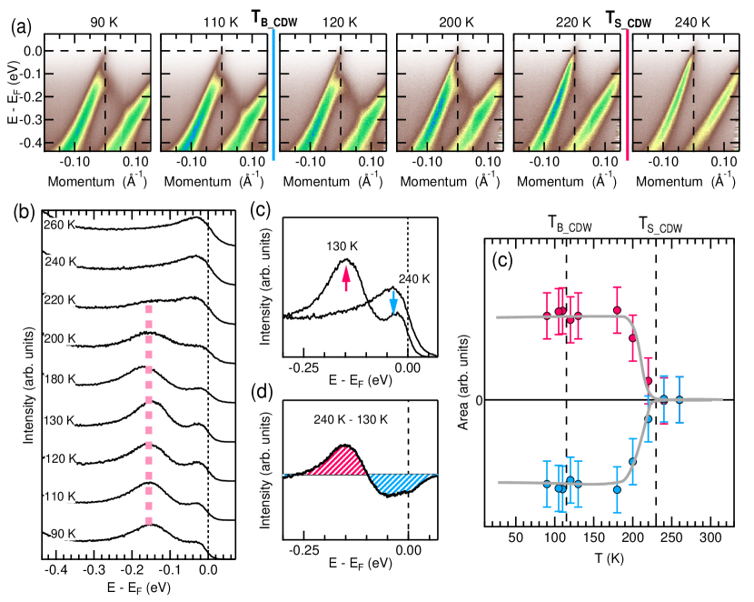
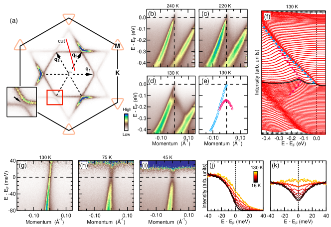
The band dispersion at temperatures well above the CDW transition is shown along a cut through the inner FS in Fig. 1b and is rather unremarkable. When the sample is cooled down to 220 K, still above the bulk transition temperature, TB_CDW, an astonishing transformation of the band dispersion occurs (Fig. 1c). The single conduction band present at high temperatures appears to split into two branches, as is even more clear at 130 K (panel d). One branch follows the high-temperature dispersion, while the other reaches only -150 meV, then bends back towards higher binding energies marking the presence of an energy gap with its minimum located at the metallic kF value. The dispersion extracted from low temperature energy distribution curve (EDC) is shown in Fig. 1e. The appearance of the lower branch coincides with the decrease of the intensity of the other branch that crosses EF. A detailed analysis of the intensities of each branch is presented in the Supplemental Material Fig. S1. The most natural explanation of this unusual behavior is that the measured band dispersion is a combination of surface and bulk contributions. The electronic structure measured at high temperature, quite surprisingly, must be very similar for both, thus we observe a single band. At lower temperatures, we attribute the conducting branch of the band to the metallic bulk of the crystal and the gapped branch to the surface of the crystal, where the gap is due to a CDW with a transition temperature of 230 K enhanced from the 115 K bulk value. Surprisingly, the energy value of the gap minimum of the surface CDW is temperature independent. Instead, the intensity of the gapped surface band increases with decreasing temperature. Such unusual behavior is likely a result of strong coupling, and is similar to cuprates Fedorov et al. (1999).
Above the bulk CDW transition, the metallic branch crosses EF as shown in Fig. 1g-k. Upon cooling below the bulk CDW TB_CDW, the intensity at EF decreases - a clear signature of the opening of an energy gap due to the bulk CDW confirmed by raw and symmetrized EDC’s (Fig. 1j,k). The temperature at which the bulk gap opens - TB_CDW=115 K and an energy of 12 meV are consistent with values expected for the bulk CDW in this material. The leading edge of the EDC’s moves to higher binding energies upon cooling, in contrast with the behavior of the large gap at the surface, where the gap energy is temperature independent and instead the gap develops by transferring spectral weight.
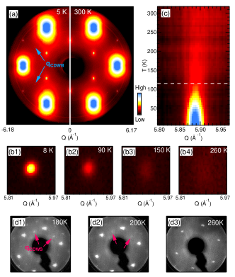
To validate these conclusions, we performed extensive low-energy electron diffraction (LEED) and x-ray studies. The LEED studies, carried out with electron energies of 54 eV, are primarily sensitive to the surface electron density, whereas the x-ray measurements, with energies of 100 keV, probe the bulk of the sample. In Fig. 2a-c we plot our x-ray data. At 5 K, we observed additional Bragg peaks, with positions consistent with the previously reported CDW superstructure Buder et al. (1982). A detailed temperature–dependent measurement of the diffraction peak with high resolution shows that the peaks sharpen and become more intense below the bulk CDW transition temperature TB_CDW (Fig. 2b and 2c). In the LEED data (Fig. 2d), clear CDW superstructure peaks occur already at 200 K, much higher than the bulk transition. A significant enhancement of the surface CDW is therefore the most likely explanation of the ARPES data.
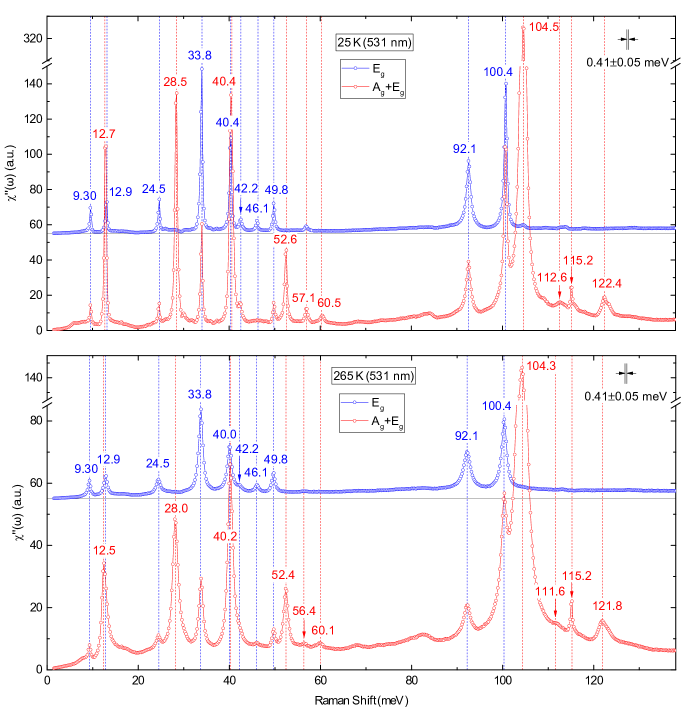
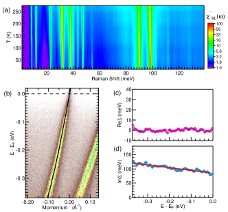
To investigate the role of phonons in the formation of the CDW we conducted temperature–dependent measurements of the phonon spectrum using Raman spectroscopy and show the results in Fig. 3a (more detailed plots can be found in the Supplementary Materials Fig. S2). The drop of the electronic background intensity below 24 meV and 115 K indicates the opening of the energy gap, consistent with the “bulk” ARPES data. However, in contrast to materials where new phonons appear in the CDW phase Holy et al. (1976); Klein (1982), no changes in the phonon energies are observed across both bulk and surface transitions for purple bronze. This absence indicates that any changes in the ionic positions across the CDW transition are likely very small and well below our detection limit.
Of course, Raman spectroscopy is only sensitive to phonons at the center of the Brillouin zone, and not all phonon modes are Raman-active. To verify our hypothesis that the el-ph coupling is weak and does not play a leading role in formation of CDW in purple bronze, we conducted a detailed study of the ARPES dispersion. This method is very sensitive to the coupling of electrons to all phonon modes, as any significant coupling is visible as kinks in the dispersion. In Fig. 3b, the black line is a parabolic fit to ARPES data over a large energy range and reflects a “bare”, non-interacting dispersion. Surprisingly, there is no evidence of deviations of the data from this line (i e. kinks), signifying the absence of strong el-ph coupling. We use the dispersion data and a parabolic fit to extract the real part of the self energy and the MDC width to obtain the imaginary part, shown in Fig. 3c and 3d respectively. Again, there is no evidence of the coupling of electrons to phonons or any other collective excitations in this material. This is in stark contrast to conventional CDW materials like NbSe2, where several such features were reported Rahn et al. (2012). Based on our ARPES data, any peaks in the real part of the self energy must be smaller than the 3 meV error bars; by constrast, MgB2 has an 80 meV peak Mou et al. (2015) and NbSe2 an 30 meV peakRahn et al. (2012). The absence of such features is highly unusual and implies that the el-ph coupling does not play significant role in the formation of the CDW, as suggested by our Raman and ARPES data.
As the combination of ARPES and Raman data seems to rule out el-ph coupling as the origin of the CDW in purple bronze, we must consider electronic mechanisms. Indeed, el-el interactions drive a CDW in the Sr14Cu24O41 ladder compounds Blumberg et al. (2002) and possibly in the cupratesHoffman et al. (2002); Kivelson et al. (2003); Berg et al. (2007); Ghiringhelli et al. (2012); Lee (2014); Wang et al. (2015). However, these systems are so strongly interacting as to be magnetic, and as a consequence, the CDW wave-vector is unrelated to nesting. However, K0.9Mo6O17 shows no signs of magnetism, and the CDW wave-vector is clearly determined by nesting, making a magnetic origin unlikely. Indeed, the FS of K0.9Mo6O17 consists of quasi-1D lines, leading to extremely good nesting, similar to the rare-earth tellurides, which also show a 2D CDW transitionMoore et al. (2010). The tellurides have strong el-ph couplingLavagnini et al. (2010); Maschek et al. (2015), but we require an alternative interaction for K0.9Mo6O17. The on-site el-el interaction is repulsive in the CDW channel, however further neighbor interactions are attractive. Normally one would not expect these in a good metal, however, the quasi-1D nature of the bands reduces the screening of the Coulomb interaction. Therefore, further neighbor interactions could stabilize a CDW at wave-vectors connecting two of the quasi-1D FSs, consistent with the wave-vectors here. The relevance of quasi-1D physics Lee et al. (1973) is also seen in the power law behavior of . has been extracted from the data (Fig. 3d) and is linear with energy at least up to 0.4 eV (highest binding energy measured). The possibility of such interactions stabilizing a CDW was examined in the related quasi-1D Li0.9Mo6O17, which similarly shows Luttinger liquid behavior Gweon et al. (2004); Chudzinski et al. (2012). Although no CDW forms, the estimated Coulomb parameters put it close to the regime where el-el interactions could induce a CDW. Thus, the CDW in K0.9Mo6O17 is likely due to el-el interactions enhanced both by strong nesting and quasi-one-dimensionality. The screening is further reduced at the surface, explaining the surface strong coupling behavior.
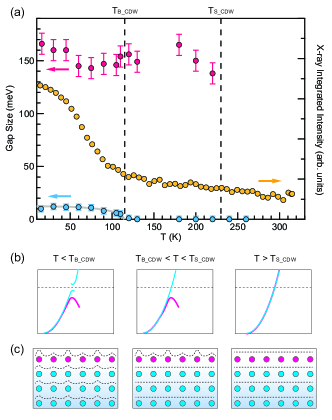
The behavior of the two energy gaps and the bulk CDW order measured by x-ray is shown in Fig. 4a. The bulk CDW gap decreases in BCS-like fashion with temperature and closes at the bulk TB_CDW=115 K, which corresponds to the dramatic decrease of the intensity of the bulk x-ray superstructure peak. The large energy gap, which we attribute to the CDW at the surface, remains open up to 230 K. The magnitude of this gap does not change with temperature, instead the spectral weight appears to be transferred to the metallic band that crosses EF. The ratio for the bulk band is 2.5, while at the surface it is in excess of 15. Combining ARPES, LEED and x-ray diffraction results, we illustrate the formation of the surface and bulk CDW and their corresponding band structures in Fig. 4b,c. As the temperature decreases, the surface layer first forms a CDW below TS_CDW (230 K) and a large gap (150 meV) appears in the surface band. The bulk CDW sets in at 115 K well below TS_CDW and a much smaller gap (12 meV) opens in a BCS-like fashion in the bulk band. Perhaps the most astonishing aspect of our results is that despite such different behavior at the surface and in the bulk, the electronic structures are essentially identical at high temperature. We observe no band splitting at any temperature. By contrast, the single layer material with enhanced TCDW has an electronic structure significantly different from its bulk counterpart Liu et al. (2012); Ugeda et al. (2015).
In summary we report the discovery of an extraordinary CDW at the surface of purple bronze that lacks any signatures of el-ph coupling and has an energy gap enhanced by more than order of magnitude from the bulk. The strong coupling, combined with dominant role of el-el interaction makes the surface charge order in purple bronze a CDW counterpart to unconventional superconductivity. Indeed, a suppression of this CDW order, if possible, may lead to an exotic superconducting state.
We gratefully acknowledge discussion with Steve Kivelson, Patrick Lee, Mike Norman and Mohit Randeria. Work at the Ames Laboratory was supported by the Department of Energy, Basic Energy Sciences, Division of Materials Sciences and Engineering, under Contract No. DE-AC02-07CH11358 (ARPES measurements). This research used resources of the Advanced Photon Source, a U.S. Department of Energy (DOE) Office of Science User Facility operated for the DOE Office of Science by Argonne National Laboratory under Contract No. DE-AC02-06CH11357 (X-ray scattering measurements). Work at Rutgers was supported by the National Science Foundation under Award NSF DMR-1104884 (Raman measurements). GB acknowledges support from the U.S. Department of Energy, Office of Basic Energy Sciences, Division of Materials Sciences and Engineering under Award DE-SC0005463 (interpretation of material behavior and reconciling information from various techniques).
References
- Grüner (1988) G. Grüner, Rev. Mod. Phys. 60, 1129 (1988).
- Valla et al. (2000) T. Valla, A. V. Fedorov, P. D. Johnson, J. Xue, K. E. Smith, and F. J. DiSalvo, Phys. Rev. Lett. 85, 4759 (2000).
- Valla et al. (2004) T. Valla, A. V. Fedorov, P. D. Johnson, P.-A. Glans, C. McGuinness, K. E. Smith, E. Y. Andrei, and H. Berger, Phys. Rev. Lett. 92, 086401 (2004).
- Yokoya et al. (2001) T. Yokoya, T. Kiss, A. Chainani, S. Shin, M. Nohara, and H. Takagi, Science 294, 2518 (2001).
- Kiss et al. (2007) T. Kiss, T. Yokoya, A. Chainani, S. Shin, T. Hanaguri, M. Nohara, and H. Takagi, Nat Phys 3, 720 (2007).
- Rahn et al. (2012) D. J. Rahn, S. Hellmann, M. Kalläne, C. Sohrt, T. K. Kim, L. Kipp, and K. Rossnagel, Phys. Rev. B 85, 224532 (2012).
- Wilson and Yoffe (1969) J. Wilson and A. Yoffe, Advances in Physics 18, 193 (1969).
- Wilson et al. (1975) J. Wilson, F. Di Salvo, and S. Mahajan, Advances in Physics 24, 117 (1975).
- Moore et al. (2010) R. G. Moore, V. Brouet, R. He, D. H. Lu, N. Ru, J.-H. Chu, I. R. Fisher, and Z.-X. Shen, Phys. Rev. B 81, 073102 (2010).
- Morris (1975) R. C. Morris, Phys. Rev. Lett. 34,, 1164 (1975).
- Nagata (1992) S. Nagata, J. Phys. Chem. Solids 53,, 1259 (1992).
- Morosan et al. (2006) E. Morosan, H. W. Zandbergen, B. S. Dennis, J. W. G. Bos, Y. Onose, T. Klimczuk, A. P. Ramirez, N. P. Ong, and R. J. Cava, Nat Phys 2, 544 (2006).
- Wagner et al. (2008) K. E. Wagner, E. Morosan, Y. S. Hor, J. Tao, Y. Zhu, T. Sanders, T. M. McQueen, H. W. Zandbergen, A. J. Williams, D. V. West, and R. J. Cava, Phys. Rev. B 78, 104520 (2008).
- Joe et al. (2014) Y. I. Joe, X. M. Chen, P. Ghaemi, K. D. Finkelstein, G. A. de la Pena, Y. Gan, J. C. T. Lee, S. Yuan, J. Geck, G. J. MacDougall, T. C. Chiang, S. L. Cooper, E. Fradkin, and P. Abbamonte, Nat Phys 10, 421 (2014).
- Hoffman et al. (2002) J. E. Hoffman, E. W. Hudson, K. M. Lang, V. Madhavan, H. Eisaki, S. Uchida, and J. C. Davis, Science 295, 466 (2002).
- Ghiringhelli et al. (2012) G. Ghiringhelli, M. Le Tacon, M. Minola, S. Blanco-Canosa, C. Mazzoli, N. B. Brookes, G. M. De Luca, A. Frano, D. G. Hawthorn, F. He, T. Loew, M. M. Sala, D. C. Peets, M. Salluzzo, E. Schierle, R. Sutarto, G. A. Sawatzky, E. Weschke, B. Keimer, and L. Braicovich, Science 337, 821 (2012).
- Chang et al. (2012) J. Chang, E. Blackburn, A. T. Holmes, N. B. Christensen, J. Larsen, J. Mesot, R. Liang, D. A. Bonn, W. N. Hardy, A. Watenphul, M. v. Zimmermann, E. M. Forgan, and S. M. Hayden, Nat Phys 8, 871 (2012).
- da Silva Neto et al. (2015) E. H. da Silva Neto, R. Comin, F. He, R. Sutarto, Y. Jiang, R. L. Greene, G. A. Sawatzky, and A. Damascelli, Science 347, 282 (2015).
- Tabis et al. (2014) W. Tabis, Y. Li, M. L. Tacon, L. Braicovich, A. Kreyssig, M. Minola, G. Dellea, E. Weschke, M. J. Veit, M. Ramazanoglu, A. I. Goldman, T. Schmitt, G. Ghiringhelli, N. Barišić, M. K. Chan, C. J. Dorow, G. Yu, X. Zhao, B. Keimer, and M. Greven, Nat Commun 5, (2014).
- Wu et al. (2012) H.-H. Wu, M. Buchholz, C. Trabant, C. Chang, A. Komarek, F. Heigl, M. Zimmermann, M. Cwik, F. Nakamura, M. Braden, and C. Schüßler-Langeheine, Nat Commun 3, 1023 (2012).
- Comin et al. (2014) R. Comin, A. Frano, M. M. Yee, Y. Yoshida, H. Eisaki, E. Schierle, E. Weschke, R. Sutarto, F. He, A. Soumyanarayanan, Y. He, M. Le Tacon, I. S. Elfimov, J. E. Hoffman, G. A. Sawatzky, B. Keimer, and A. Damascelli, Science 343, 390 (2014).
- da Silva Neto et al. (2014) E. H. da Silva Neto, P. Aynajian, A. Frano, R. Comin, E. Schierle, E. Weschke, A. Gyenis, J. Wen, J. Schneeloch, Z. Xu, S. Ono, G. Gu, M. Le Tacon, and A. Yazdani, Science 343, 393 (2014).
- Hanaguri et al. (2004) T. Hanaguri, C. Lupien, Y. Kohsaka, D.-H. Lee, M. Azuma, M. Takano, H. Takagi, and J. C. Davis, Nature 430, 1001 (2004).
- Vershinin et al. (2004) M. Vershinin, S. Misra, S. Ono, Y. Abe, Y. Ando, and A. Yazdani, Science 303, 1995 (2004).
- Le Tacon et al. (2014) M. Le Tacon, A. Bosak, S. M. Souliou, G. Dellea, T. Loew, R. Heid, K.-P. Bohnen, G. Ghiringhelli, M. Krisch, and B. Keimer, Nat Phys 10, 52 (2014).
- Reznik et al. (2006) D. Reznik, L. Pintschovius, M. Ito, S. Iikubo, M. Sato, H. Goka, M. Fujita, K. Yamada, G. D. Gu, and J. M. Tranquada, Nature 440, 1170 (2006).
- d’Astuto et al. (2002) M. d’Astuto, P. K. Mang, P. Giura, A. Shukla, P. Ghigna, A. Mirone, M. Braden, M. Greven, M. Krisch, and F. Sette, Phys. Rev. Lett. 88, 167002 (2002).
- Kivelson et al. (2003) S. A. Kivelson, I. P. Bindloss, E. Fradkin, V. Oganesyan, J. M. Tranquada, A. Kapitulnik, and C. Howald, Rev. Mod. Phys. 75, 1201 (2003).
- Berg et al. (2007) E. Berg, E. Fradkin, E. A. Kim, S. A. Kivelson, V. Oganesyan, J. M. Tranquada, and S. C. Zhang, Physical Review Letters 99, 127003 (2007).
- Lee (2014) P. A. Lee, Phys. Rev. X 4, 031017 (2014).
- Wang et al. (2015) Y. Wang, D. F. Agterberg, and A. Chubukov, Phys. Rev. Lett. 114, 197001 (2015).
- Blumberg et al. (2002) G. Blumberg, P. Littlewood, A. Gozar, B. S. Dennis, N. Motoyama, H. Eisaki, and S. Uchida, Science 297, 584 (2002).
- Rosen et al. (2013) J. A. Rosen, R. Comin, G. Levy, D. Fournier, Z.-H. Zhu, B. Ludbrook, C. N. Veenstra, A. Nicolaou, D. Wong, P. Dosanjh, Y. Yoshida, H. Eisaki, G. R. Blake, F. White, T. T. M. Palstra, R. Sutarto, F. He, A. Fraño Pereira, Y. Lu, B. Keimer, G. Sawatzky, L. Petaccia, and A. Damascelli, Nat Commun 4, (2013).
- McMillan (1976) W. L. McMillan, Phys. Rev. B 14, 1496 (1976).
- Brown et al. (2005) S. E. Brown, E. Fradkin, and S. A. Kivelson, Phys. Rev. B 71, 224512 (2005).
- Qing-Yan et al. (2012) W. Qing-Yan, L. Zhi, Z. Wen-Hao, Z. Zuo-Cheng, Z. Jin-Song, L. Wei, D. Hao, O. Yun-Bo, D. Peng, C. Kai, W. Jing, S. Can-Li, H. Ke, J. Jin-Feng, J. Shuai-Hua, W. Ya-Yu, W. Li-Li, C. Xi, M. Xu-Cun, and X. Qi-Kun, Chinese Physics Letters 29, 037402 (2012).
- Liu et al. (2012) D. Liu, W. Zhang, D. Mou, J. He, Y.-B. Ou, Q.-Y. Wang, Z. Li, L. Wang, L. Zhao, S. He, Y. Peng, X. Liu, C. Chen, L. Yu, G. Liu, X. Dong, J. Zhang, C. Chen, Z. Xu, J. Hu, X. Chen, X. Ma, Q. Xue, and X. Zhou, Nat Commun 3, 931 (2012).
- Xi et al. (2015) X. Xi, L. Zhao, Z. Wang, H. Berger, L. Forró, J. Shan, and K. F. Mak, Nat Nano advance online publication, (2015).
- Lee et al. (2014) J. J. Lee, F. T. Schmitt, R. G. Moore, S. Johnston, Y.-T. Cui, W. Li, M. Yi, Z. K. Liu, M. Hashimoto, Y. Zhang, D. H. Lu, T. P. Devereaux, D.-H. Lee, and Z.-X. Shen, Nature 515, 245 (2014).
- Calandra et al. (2009) M. Calandra, I. I. Mazin, and F. Mauri, Phys. Rev. B 80, 241108 (2009).
- Greenblatt (1988) M. Greenblatt, Chem. Rev. 88, 31 (1988).
- Buder et al. (1982) R. Buder, J. Devenyi, J. Dumas, J. Marcus, J. Mercier, C. Schlenker, and H. Vincent, J. Physique Lett. 43, 59 (1982).
- Vincent et al. (1983) H. Vincent, M. Ghedira, J. Marcus, J. Mercier, and C. Schlenker, Journal of Solid State Chemistry 47, 113 (1983).
- Whangbo et al. (1991) M. H. Whangbo, E. Canadell, P. Foury, and J. P. Pouget, Science 252, 96 (1991).
- Gweon et al. (1997) G. H. Gweon, J. W. Allen, J. A. Clack, Y. X. Zhang, D. M. Poirier, P. J. Benning, C. G. Olson, J. Marcus, and C. Schlenker, Phys. Rev. B 55, R13353 (1997).
- Escribe-filippini et al. (1984) C. Escribe-filippini, K. Konaté, J. Marcus, C. Schlenker, R. Almairac, R. Ayroles, and C. Roucau, Philosophical Magazine Part B 50, 321 (1984).
- Mallet et al. (1999) P. Mallet, K. M. Zimmermann, P. Chevalier, J. Marcus, J. Y. Veuillen, and J. M. G. Rodriguez, Phys. Rev. B 60, 2122 (1999).
- Xiong et al. (2001) R. Xiong, M. Tian, H. Liu, W. Tang, M. Jing, J. Sun, Q. Kou, D. Tian, and J. Shi, Materials Science and Engineering: B 87, 191 (2001).
- Jiang et al. (2014) R. Jiang, D. Mou, Y. Wu, L. Huang, C. D. McMillen, J. Kolis, H. G. Giesber, J. J. Egan, and A. Kaminski, Review of Scientific Instruments 85, 033902 (2014).
- Fedorov et al. (1999) A. V. Fedorov, T. Valla, P. D. Johnson, Q. Li, G. D. Gu, and N. Koshizuka, Phys. Rev. Lett. 82, 2179 (1999).
- Holy et al. (1976) J. A. Holy, M. V. Klein, W. L. McMillan, and S. F. Meyer, Phys. Rev. Lett. 37, 1145 (1976).
- Klein (1982) M. V. Klein, Phys. Rev. B 25, 7192 (1982).
- Mou et al. (2015) D. Mou, R. Jiang, V. Taufour, R. Flint, S. L. Bud’ko, P. C. Canfield, J. S. Wen, Z. J. Xu, G. Gu, and A. Kaminski, Phys. Rev. B 91, 140502 (2015).
- Lavagnini et al. (2010) M. Lavagnini, H.-M. Eiter, L. Tassini, B. Muschler, R. Hackl, R. Monnier, J.-H. Chu, I. R. Fisher, and L. Degiorgi, Phys. Rev. B 81, 081101 (2010).
- Maschek et al. (2015) M. Maschek, S. Rosenkranz, R. Heid, A. H. Said, P. Giraldo-Gallo, I. R. Fisher, and F. Weber, Phys. Rev. B 91, 235146 (2015).
- Lee et al. (1973) P. A. Lee, T. M. Rice, and P. W. Anderson, Phys. Rev. Lett. 31, 462 (1973).
- Gweon et al. (2004) G.-H. Gweon, S.-K. Mo, J. W. Allen, J. He, R. Jin, D. Mandrus, and H. Höchst, Phys. Rev. B 70, 153103 (2004).
- Chudzinski et al. (2012) P. Chudzinski, T. Jarlborg, and T. Giamarchi, Phys. Rev. B 86, 075147 (2012).
- Ugeda et al. (2015) M. M. Ugeda, A. J. Bradley, Y. Zhang, S. Onishi, Y. Chen, W. Ruan, C. Ojeda-Aristizabal, H. Ryu, M. T. Edmonds, H.-Z. Tsai, A. Riss, S.-K. Mo, D. Lee, A. Zettl, Z. Hussain, Z.-X. Shen, and M. F. Crommie, Nat Phys advance online publication, (2015).
I Supplemental Material for Discovery of unconventional charge density wave at the surface of K0.9Mo6O17
II SAMPLES
K0.9Mo6O17 single crystals were grown by electrolytic reduction. K2CO3 and MoO3 mixed power with molar ratio of 1:6 was melt at 580∘C in an alumina crucible and an electric current of 40 mA was applied through the melt by platinum wire electrodes. Single crystals were obtained on the cathode after three hours. The typical size of the samples was mm3 in ARPES measurements and mm3 in the x-ray diffraction measurements.
III ARPES
Samples were cleaved in situ at a base pressure lower than 8 10-11 Torr. They were cooled using a closed cycle He-refrigerator and the sample temperature was measured using a silicon-diode sensor mounted on the sample holder. The energy corresponding to the chemical potential was determined from the Fermi edge of a polycrystalline Au reference in electrical contact with the sample. Samples were cleaved at three temperatures (40 K, 130 K and 260 K) to check the stability of the surface structure.
IV XRAY
Two-dimensional diffraction patterns of the (H K 0) reciprocal plane were measured for overview using a MAR345 detector after rocking the sample through two independent angles up to 1.8∘ about axes perpendicular to the incident beam. The sample was mounted on the cold finger of an APD He closed–cycle refrigerator. A detailed study of the temperature dependence of the ( 0 0) CDW Bragg peak was performed using the high-resolution Pixirad detector by rocking the sample through one angle by 5∘. The integrated intensity of the CDW peaks was obtained from fitting two-dimensional Gaussian peaks.
V RAMAN
The sample was cooled with a continuous flow liquid helium cryostat, and the temperatures quoted have been corrected for the laser heating. We used a custom triple-grating spectrometer and liquid nitrogen cooled CCD for analysis and collection of the scattered light. The K0.9Mo6O17 compound crystallizes in a trigonal structure belonging to the point group (space group P, No. 147) Vincent et al. (1983). The structure allows a total of 48 phonon modes at the Brillouin zone center ( point), categorized by the irreducible representations of the group: acoustic modes, infrared active optical phonons, and Raman active phonons. The Raman response function, , measures the electronic and phononic excitations with symmetry ( group) when the scattered photon are analyzed in the polarization perpendicular to the incident laser polarization, which is aligned with the crystallographic -axis, whereas excitations with symmetry ( group) are probed when the scattered photon are analyzed in the polarization parallel to the incident laser polarization.
