Thermoelectric detection of propagating plasmons in graphene
Controlling, detecting and generating propagating plasmons by all-electrical means is at the heart of on-chip nano-optical processing.Gramotnev & Bozhevolnyi (2010); Vakil & Engheta (2011); Dyakonov & Shur (1996) Graphene carries long-lived plasmons that are extremely confined and controllable by electrostatic fields,Wunsch et al. (2006); Hwang & Das Sarma (2007); Jablan et al. (2009); Grigorenko et al. (2012) however electrical detection of propagating plasmons in graphene has not yet been realized. Here, we present an all-graphene mid-infrared plasmon detector, where a single graphene sheet serves simultaneously as the plasmonic medium and detector. Rather than achieving detection via added optoelectronic materials, as is typically done in other plasmonic systems,Ditlbacher et al. (2006); Neutens et al. (2009); Falk et al. (2009); Heeres et al. (2010); Dufaux et al. (2010); Goykhman et al. (2011); Goodfellow et al. (2015); Brongersma et al. (2015) our device converts the natural decay product of the plasmon—electronic heat—directly into a voltage through the thermoelectric effect.Innes & Sambles (1985); Weeber et al. (2011) We employ two local gates to fully tune the thermoelectric and plasmonic behaviour of the graphene. High-resolution real-space photocurrent maps are used to investigate the plasmon propagation and interference, decay, thermal diffusion, and thermoelectric generation.
Graphene plasmonics is an emerging platform for terahertz to infrared nano-optics, attractive due to the long intrinsic lifetime of ps and the strong tunable broadband electrodynamic response of its Dirac electrons.Jablan et al. (2009); Principi et al. (2014) Typically, graphene plasmons are sensed by out-coupling to light, which is inefficient due to one of the key features of graphene plasmons: their extremely short wavelength ( that of free space light). While plasmon resonances have been exploited to enhance absorption and thereby enhance far-field photodetection,Freitag et al. (2013); Cai et al. (2015) the concept of an on-chip plasmon receiver has not yet been realized.
The presented experimental device is built around the state-of-the-art plasmonic medium of graphene encapsulated in hexagonal boron nitride (hBN), which we have recently demonstrated to support high quality propagating plasmons in the mid infrared.Woessner et al. (2014) As a key innovation in this work, the induction of free carriers in the graphene is achieved through the use of separate local gates directly underneath the hBN, rather than the conventional global back gating through an additional SiO2 layer. The use of local gating allows to spatially modulate the charge carrier density and polarity across the device, as well as providing lower voltage operation and reduced charge trapping effects.Woessner et al. (2015) As we will show below, the junction induced by the two gates can be used as a thermoelectric detector for the plasmons.
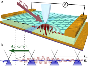
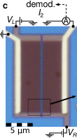
Figures 1a,b show a schematic of the operating principle of the detector. In lieu of an on-chip plasmon source, we generate plasmons using the conventional scattering scanning near field microscopy (s-SNOM) technique.Fei et al. (2012); Chen et al. (2012) The s-SNOM apparatus consists of a scanning metal probe under illumination from a continuous wave laser at mid infrared frequency. A laser frequency of 28 THz ( free space wavelength) was chosen to avoid complications from the hBN phonons.Woessner et al. (2014) In conventional plasmonic s-SNOM experiments, the signal of interest is the out-scattered light, containing information about local dielectric properties and plasmonic modes. Here, we instead measure a quantity , known as near field photocurrent, from the current exiting the device electrodes (Fig. 1c).Woessner et al. (2015) This is the component of total measured current that oscillates at the second harmonic (500 kHz) of the probe tapping frequency (250 kHz). As the graphene shows a linear photocurrent response, can be understood as the photocurrent arising only from the 60 nm-sharp near fields of the tip, isolated from the background photocurrent directly induced by the incident light. For simplicity, in the remainder of this paper we refer to simply as “the photocurrent” and treat it as if it arises from an effective nanoscale light source.
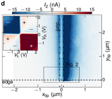
The studied device and circuit schematic is shown in Fig. 1c. By applying different voltages to the left (right) gates, we induce a localized photosensitive region, e.g., a – junction as studied in Fig. 1d. The six-fold photocurrent pattern observed when both gates are scanned (figure inset) is considered as evidence of a thermoelectric generation mechanism, where the pattern arises due to the nonmonotonic dependence of Seebeck coefficient on gate voltage.Xu et al. (2010); Lemme et al. (2011); Song et al. (2011); Gabor et al. (2011) For a simple junction, the thermoelectric current is , where is the left (right) Seebeck coefficient, is the junction-average rise in electronic temperature relative to ambient, and is the circuit resistance. The gate dependence allows to identify the charge neutrality point of the graphene in this device (occuring at a gate voltage offset of +0.09 V). Hereafter we use this offset and the calculated gate capacitance to convert the gate voltages into carrier densities .
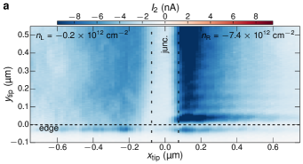
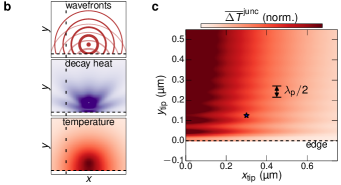
Strong evidence of plasmons mediating the photocurrent is visible in photocurrent maps obtained at high carrier density (Fig. 2a), where interference fringes can be observed in near the graphene edge. These fringes can be unambiguously attributed to plasmon reflections, as they match the half-wavelength periodicity seen in the s-SNOM optical signal that is conventionally used to characterize graphene plasmons.Woessner et al. (2014) The extracted plasmon wavelength of nm in this scan is close to the expected value of 114 nm, and consistent with a previous study of a similar hBN–graphene–hBN device.Woessner et al. (2014)
To explain the spatial pattern and the detection mechanism, we consider the following sequence, sketched in Fig. 2b: Plasmons radiate away from the tip and reflect at the edge; the self-interfered plasmon wave decays into electronic heat; subsequent electronic diffusion spreads the heat to the junction, determining . To justify this interpretation, we employ a simplified two-dimensional model that takes into account each of these effects. The model, detailed in Methods, yields the value of (up to a normalization) for a plasmon source located at any position , . The three critical model parameters are plasmon wavevector , reflection coefficient , and electron cooling length . By varying these, we obtain a map (Fig. 2c) that fits to the data, capturing the essential physics behind the observed spatial pattern. Note that this model neglects direct three-dimensional near field coupling effects, giving some disagreement within nm of the edge and junction.
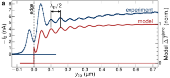
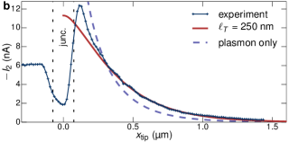
Two complex parameters, and , are key for matching the dependence, examined in detail in Fig. 3a. Whereas determines the fringe spacing, encodes the plasmon decay length and determines the number of visible fringes. In particular, the fringes decay according to an envelope function , identical to that of the optical signal.Woessner et al. (2014) The reflection coefficient is relevant for setting the overall magnitude and phase of the fringes, from and respectively. The subunity value of also leads to a drop in power as the tip is brought near the edge, since in this model the unreflected plasmon power is lost. A similar drop is seen in the data, suggesting that the unreflected plasmon power is not converted to electronic heat in the same way as for plasmon decay elsewhere.
The electron cooling length, , is important for matching the photocurrent decay away from the junction, shown in Fig. 3b. This is the typical distance of electronic thermal diffusion before the heat is conducted out of the electronic system, and hence correponds to the effective length over which the junction is sensitive to heat inputs (in this case, plasmon decay heat). At this point it is worthwhile to compare to other hypothetical non-thermal detection mechanisms, where the junction would sense directly the incident plasmon power. In that case, the signal would be proportional to the average plasmon intensity precisely at the junction, and hence proportional to the un-diffused decay heat along the junction. As we show in Fig. 3b, such mechanisms would produce a too-short decay length, determined only by the plasmon energy propagation length, .
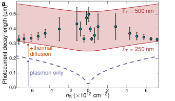
The requirement of some diffusion to match the data confirms our picture that the detection mechanism does not rely on direct rectification of the plasmon at the junction, but instead is based on sensing the temperature rise from plasmon decay. Further evidence along this line is shown in Fig. 4a, where we have analyzed the photocurrent decay by a fitted exponential decay length, at several different carrier densities. This dependence disagrees both quantitatively and qualitatively with a direct detection mechanism. Instead, a density-dependent value of from nm (low ) to nm (high ) is needed.
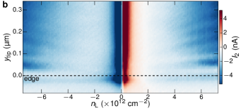
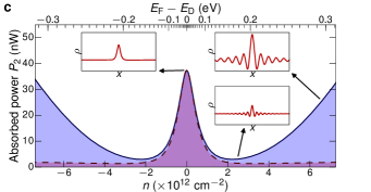
Next, we show tunability of the nature and strength of the plasmon launching, with varying carrier density (Figs. 4b,c). Figure 4b shows the dependence of the photocurrent on the gate voltage under the tip. The data show several features simultaneously evolving with carrier density. There are two sign changes in photocurrent, due to the sign change of Seebeck coefficient differences.Xu et al. (2010); Lemme et al. (2011); Song et al. (2011); Gabor et al. (2011) The fringe spacing appears to follow as expected for graphene plasmons.Woessner et al. (2014) Most strikingly, the photocurrent shows two regimes of strong magnitude, at high and low , separated by a region of weak photocurrent from –. We attribute these to the two ways that graphene can absorb power from the tip: direct heating or plasmon launching, which are both captured in our quantitative electrodynamic calculations of the absorbed power (Fig. 4c, details in Methods). The launched plasmon power grows strongly with carrier density primarily due to variation in plasmon wavelength: plasmons with small values of couple poorly to the tip due to their strong confinement in the top hBN layer and the limited range of spatial frequencies probed by the round tip. Direct heating on the other hand is strongest for low due to unblocked interband transitions, possible when the Dirac point is within about ( meV) of the Fermi level .
The observed photocurrent signals are well above the noise level, and according to the calculation of Fig. 4c these signals arise from a plasmon power of order 10 nW—note that there is some uncertainty in this number due to the difficulty of accurately modelling the tip. This order-of-magnitude power estimate can be compared to that predicted for local plasmon sources, to see whether such compact sources could serve in place of our plasmon-launching tip. One proposed plasmon source is the graphene thermal plasmon radiator,Liu et al. (2014) which is a hot graphene strip (at K) adjacent to a room temperature graphene channel. Such a source would emit plasmon power on the order of tens of nanowatts,Liu et al. (2014) which should be detectable using our junction device.
In conclusion, we have shown that a graphene homojunction serves as an electrical detector for the mid-infrared plasmons that are carried by the graphene itself. The available evidence strongly indicates that thermoelectric action is detecting the energy of the plasmon after it has decayed and that thermal diffusion plays an important role in spreading the decay energy. The presented concept opens the door to graphene plasmonic devices where inefficient plasmon out-coupling to light is unnecessary. We anticipate in the future that this detector may be paired with a local plasmon source such as those based on thermalLiu et al. (2014) or tunneling emission,Svintsov et al. (2015) resulting in an end-to-end mid infrared optical system at sizes far below the light diffraction limit.
Methods
Device fabrication started with an 10 nm, surface low roughness AuPd alloy gate film patterned by electron beam lithography, on top of an oxidized Si substrate. The gap separating the gates from each other was 150 nm, as indicated in the figures. An hBN–graphene–hBN stack was then prepared by the van der Waals assembly technique,Wang et al. (2013) and placed on top of the AuPd gate layer. The bottom hBN film (between graphene and metal) thickness of 27 nm was chosen to isolate the plasmonic mode from interacting with the gate metal, while still allowing for strong gate effect. The top hBN film was made thin (9 nm) to allow for plasmon launching by the s-SNOM method. The device geometry as well as the edge contacts were defined by dry etching and electron beam evaporation in the method of Ref. Wang et al., 2013. The dry etching depth was only 11 nm, leaving most of the bottom hBN thickness remaining in order to avoid leakage. Gate voltages were converted to carrier sheet density via , where the offset was determined by examining gate dependences and the coefficient was calculated as the static capacitance of the 27 nm hBN layer with dielectric constant 3.56.Woessner et al. (2014)
The s-SNOM used was a NeaSNOM from Neaspec GmbH, equipped with a CO2 laser. The probes were commercially-available metallized atomic force microscopy probes with an apex radius of approximately 25 nm. The tip height was modulated at a frequency of approximately with amplitude of 60 nm. The location of the etched graphene edge () was determined from the simultaneously-measured topography.Woessner et al. (2014)
In Fig. 2, we solve the Helmholtz wave equation
| (1) |
for a localized sourcing distribution (concentrated at , ), where is the complex plasmon wavevector. Here represents the spatial dependence of the oscillating charge density . The reflective boundary at is asserted by the method of images: solving (1) for free space, adding a virtual copy at multiplied by a complex reflection coefficient , and discarding the virtual solution below . Dissipation in the graphene converts the plasmon to a decay heat distribution proportional to . This heating distribution is diffused,
| (2) |
to yield , the local temperature distribution, with edge boundary condition . The parameter is the characteristic length of lateral heat spreading before sinking to the substrate at temperature . Finally the average temperature rise on the junction, which drives the thermoelectric effect, is represented by the quantity :
| (3) |
for device width , and it is this quantity plotted in Fig. 2c. The value of , strength of , and other proportionality factors drop out due to normalization. The case of direct plasmon detection is found in the limit , in which case the signal is determined by the -integral of .
The solid curves in Figure 4a result from performing an exponential fit to the modelled . For each we estimated using the fitted from high (Figs. 2,3) and the trend found in our previous study.Woessner et al. (2014)
Our electrodynamic calculation (Fig. 4c) consists of a tip charge distribution, calculated via a regularized boundary-element electrostatic model,McLeod et al. (2014) fed into a multilayer transfer matrix calculation for the hBN–graphene–hBN-metal stack. An incident field of 0.3 MV/m was estimated from the experimental 10 mW incident laser power, which is focussed to a diffraction-limited spot (NA 0.5, wavelength). The tip surface was taken as a circular hyperboloid of opening angle and a 25 nm curvature radius at the apex, with a length yielding a 45 tip electric field enhancement factor over the incident field. The 3D charge distribution was remapped to a 2D charge distribution located a distance from the top hBN surface and this distribution was oscillated at 28 THz, with accompanying in-plane currents. The absorbed power in the graphene, , was calculated for 36 different values from 0 to 60 nm, and this height dependence was then used to simulate the second harmonic demodulation process, arriving at a second-harmonic power that best corresponds to the studied current . The hBN relative permittivity at this frequency was taken as in-plane and out-of-plane.Woessner et al. (2014) The graphene conductivity used was the local finite-temperature RPA conductivity formula,Falkovsky & Varlamov (2007) taking care to map from to using the appropriate Fermi-Dirac integral.
Acknowledgements.
We thank Marco Polini, Alexey Nikitin, and Klaas-Jan Tielrooij for fruitful discussions. This work used open source software (www.matplotlib.org, www.python.org, www.povray.org). F.H.L.K. and R.H. acknowledge support by the EC under Graphene Flagship (contract no. CNECT-ICT-604391). F.H.L.K. acknowledges support by Fundacio Cellex Barcelona, the ERC Career integration grant (294056, GRANOP), the ERC starting grant (307806, CarbonLight), the Government of Catalonia trough the SGR grant (2014-SGR-1535), the Mineco grants Ramón y Cajal (RYC-2012-12281) and Plan Nacional (FIS2013-47161-P). P.A.-G. and R.H. acknowledge support from the European Union through ERC starting grant (TERATOMO grant no. 258461) and the Spanish Ministry of Economy and Competitiveness (national project MAT2012-36580). Y.G., C.T., and J.H. acknowledge support from the US Office of Naval Research N00014-13-1-0662.References
- Gramotnev & Bozhevolnyi (2010) Gramotnev, D. K. & Bozhevolnyi, S. I. Plasmonics beyond the diffraction limit. Nature Photon. 4, 83–91 (2010).
- Vakil & Engheta (2011) Vakil, A. & Engheta, N. Transformation optics using graphene. Science 332, 1291–1294 (2011).
- Dyakonov & Shur (1996) Dyakonov, M. & Shur, M. Detection, mixing, and frequency multiplication of terahertz radiation by two-dimensional electronic fluid. IEEE Trans. Electron Dev. 43, 380–387 (1996).
- Wunsch et al. (2006) Wunsch, B., Stauber, T., Sols, F. & Guinea, F. Dynamical polarization of graphene at finite doping. New J. Phys. 8, 318–318 (2006).
- Hwang & Das Sarma (2007) Hwang, E. H. & Das Sarma, S. Dielectric function, screening, and plasmons in two-dimensional graphene. Phys. Rev. B 75, 205418 (2007).
- Jablan et al. (2009) Jablan, M., Buljan, H. & Soljačić, M. Plasmonics in graphene at infrared frequencies. Phys. Rev. B 80, 245435 (2009).
- Grigorenko et al. (2012) Grigorenko, A. N., Polini, M. & Novoselov, K. S. Graphene plasmonics. Nature Photon. 6, 749–758 (2012).
- Ditlbacher et al. (2006) Ditlbacher, H. et al. Organic diodes as monolithically integrated surface plasmon polariton detectors. Appl. Phys. Lett. 89, 161101 (2006).
- Neutens et al. (2009) Neutens, P., Van Dorpe, P., De Vlaminck, I., Lagae, L. & Borghs, G. Electrical detection of confined gap plasmons in metal–insulator–metal waveguides. Nature Photon. 3, 283–286 (2009).
- Falk et al. (2009) Falk, A. L. et al. Near-field electrical detection of optical plasmons and single-plasmon sources. Nature Phys. 5, 475–479 (2009).
- Heeres et al. (2010) Heeres, R. W. et al. On-chip single plasmon detection. Nano Lett. 10, 661–664 (2010).
- Dufaux et al. (2010) Dufaux, T., Dorfmüller, J., Vogelgesang, R., Burghard, M. & Kern, K. Surface plasmon coupling to nanoscale Schottky-type electrical detectors. Appl. Phys. Lett. 97, 161110 (2010).
- Goykhman et al. (2011) Goykhman, I., Desiatov, B., Khurgin, J., Shappir, J. & Levy, U. Locally oxidized silicon surface-plasmon Schottky detector for telecom regime. Nano Lett. 11, 2219–2224 (2011).
- Goodfellow et al. (2015) Goodfellow, K. M., Chakraborty, C., Beams, R., Novotny, L. & Vamivakas, A. N. Direct on-chip optical plasmon detection with an atomically thin semiconductor. Nano Lett. 15, 5477–5481 (2015).
- Brongersma et al. (2015) Brongersma, M. L., Halas, N. J. & Nordlander, P. Plasmon-induced hot carrier science and technology. Nature Nanotech. 10, 25–34 (2015).
- Innes & Sambles (1985) Innes, R. & Sambles, J. Simple thermal detection of surface plasmon-polaritons. Solid State Commun. 56, 493–496 (1985).
- Weeber et al. (2011) Weeber, J.-C. et al. Thermo-electric detection of waveguided surface plasmon propagation. Appl. Phys. Lett. 99, 031113 (2011).
- Principi et al. (2014) Principi, A. et al. Plasmon losses due to electron-phonon scattering: The case of graphene encapsulated in hexagonal boron nitride. Phys. Rev. B 90, 165408 (2014).
- Freitag et al. (2013) Freitag, M. et al. Photocurrent in graphene harnessed by tunable intrinsic plasmons. Nat. Commun. 4, 1951 (2013).
- Cai et al. (2015) Cai, X. et al. Plasmon-enhanced terahertz photodetection in graphene. Nano Lett. 15, 4295–4302 (2015).
- Woessner et al. (2014) Woessner, A. et al. Highly confined low-loss plasmons in graphene–boron nitride heterostructures. Nature Mater. 14, 421–425 (2014).
- Woessner et al. (2015) Woessner, A. et al. Near-field photocurrent nanoscopy on bare and encapsulated graphene. eprint arXiv:1508.07864 (2015).
- Fei et al. (2012) Fei, Z. et al. Gate-tuning of graphene plasmons revealed by infrared nano-imaging. Nature 487, 82–85 (2012).
- Chen et al. (2012) Chen, J. et al. Optical nano-imaging of gate-tunable graphene plasmons. Nature 487, 77–81 (2012).
- Xu et al. (2010) Xu, X., Gabor, N. M., Alden, J. S., van der Zande, A. M. & McEuen, P. L. Photo-thermoelectric effect at a graphene interface junction. Nano Lett. 10, 562–566 (2010).
- Lemme et al. (2011) Lemme, M. C. et al. Gate-activated photoresponse in a graphene p–n junction. Nano Lett. 11, 4134–4137 (2011).
- Song et al. (2011) Song, J. C. W., Rudner, M. S., Marcus, C. M. & Levitov, L. S. Hot carrier transport and photocurrent response in graphene. Nano Lett. 11, 4688–4692 (2011).
- Gabor et al. (2011) Gabor, N. M. et al. Hot carrier-assisted intrinsic photoresponse in graphene. Science 334, 648–652 (2011).
- Liu et al. (2014) Liu, B., Liu, Y. & Shen, S. Thermal plasmonic interconnects in graphene. Phys. Rev. B 90, 195411 (2014).
- Svintsov et al. (2015) Svintsov, D., Devizorova, Z., Otsuji, T. & Ryzhii, V. Emission and amplification of surface plasmons in resonant - tunneling van der waals heterostructures. eprint arXiv:1509.03776 (2015).
- Wang et al. (2013) Wang, L. et al. One-dimensional electrical contact to a two-dimensional material. Science 342, 614–617 (2013).
- McLeod et al. (2014) McLeod, A. S. et al. Model for quantitative tip-enhanced spectroscopy and the extraction of nanoscale-resolved optical constants. Phys. Rev. B 90, 085136 (2014).
- Falkovsky & Varlamov (2007) Falkovsky, L. A. & Varlamov, A. A. Space-time dispersion of graphene conductivity. Eur. Phys. J. B 56, 281–284 (2007).