Dimensionality effects on the luminescence properties of hBN
Dimensionality effects on the luminescence properties of hBN
Abstract
Cathodoluminescence (CL) experiments at low temperature have been undertaken on various bulk and exfoliated hexagonal boron nitride (hBN) samples. Different bulk crystals grown from different synthesis methods have been studied. All of them present the same so-called S series in the 5.6–6 eV range, proving its intrinsic character. Luminescence spectra of flakes containing 100 down to 6 layers have been recorded. Strong modifications in the same UV range are observed and discussed within the general framework of 2D exciton properties in lamellar crystals.
pacs:
71.20.Nr, 71.55.Eq, 71.35.-y, 73.21.Ac, 78.55.CrI Introduction
Black and white graphenes are one-atom thick layers of graphite and hexagonal boron nitride (hBN), respectively. Their remarkable properties are inherited from their two-dimensional (2D) crystal structure and symmetry: Graphene is a semi-metal populated by massless chiral Dirac fermions while hBN is a large band gap semiconductor ( 6 eV). As an ultimate 2D crystal, single-layer graphene (SLG) is highly sensitive to its environment and its unique properties can easily be spoiled, but may also be enhanced by the close proximity of a substrate. Therefore, having mostly understood the potential of intrinsic graphene, the new challenge is to engineer its coupling to substrates Ju et al. (2014); Woods et al. (2014) and exploit it to realize innovative electronic and optoelectronic devices. It has become quite clear in recent years that the most compatible environment for graphene is hBN, due to both its insulating character and its similar honeycomb crystal structure, which matches almost perfectly that of graphene.Dean et al. (2010); Wang et al. (2013); Mishchenko et al. (2014) Further graphene and hBN have excellent material characteristics, in particular a strong bonding that sets a robust energy scale for all excitations (electrons, phonons, excitons).
The rise in widely using hBN layers as a substrate or encapsulating layers of graphene is mainly based on their ability to preserve at the best electronic properties of graphene such as the carrier mobility. Dean et al. (2010) However, it was recently shown that, when graphene is epitaxially stacked on hBN layers, a strong interlayer coupling can arise, resulting in marked modifications of its electronic properties. Yankowitz et al. (2012); Yang et al. (2013) An appropriate control of the quality and properties of hBN layers, which may be in turn in an interlayer coupling seems, therefore, an essential milestone towards an appropriate use of hBN layers in complex heterostructure architectures and devices.
However, in contrast to graphene, electronic properties of BN materials remain basically to understand. Luminescence spectroscopies are here very useful tools. Dedicated cathodoluminescence (CL) and photoluminescence (PL) experiments at 10K have been recently developed and used to study BN powders, single crystals and nanotubes.Watanabe et al. (2004, 2006a, 2006b); Silly et al. (2007); Jaffrennou et al. (2008); Pierret et al. (2014, 2015)
Luminescence of hBN is found to be dominated by near band edge excitonic recombinations, described as S and D lines. The higher-energy S lines, between 5.6 and 5.9 eV, are generally attributed to intrinsic free excitons, whereas the lower-energy D ones, between 5.4 and 5.65 eV, are assigned to excitons trapped in structural defects.Jaffrennou et al. (2007); Watanabe and Taniguchi (2009) Very little is known on hBN 2D layers. In 2D crystals, the excitonic effects are generally amplified by the spatial confinement of electrons and holes, and by the decrease of the electrostatic screening. Lamellar crystals have totally original features when compared to standard 3D-semiconductors, even in the confinement regime reached with epitaxial quantum wells. For instance in MoS2, the band structure evolves from an indirect bandgap in bulk crystals to a direct band gap for the single atomic layer Mak et al. (2010) having a 1 eV exciton binding energy.Qiu et al. (2013) More recently, a similar indirect-to-direct gap crossover has been reported in WS2 and WSe2 from few-layer flakes to the single-layer.Zhao et al. (2012) Analogous effects are then expected for hBN for which exciton binding energies up to 2.1 eV have been theoretically predicted for the single layer.Arnaud et al. (2006, 2008); Wirtz et al. (2005, 2006, 2008)
Here, we present a study of the luminescence properties of hBN from its bulk form to atomic exfoliated thin flakes. A thorough investigation by cathodoluminescence (CL) at 10 K of different hBN bulk sources is used to highlight the intrinsic origin of the S series. On the basis of our previous experiments,Pierret et al. (2014) we manage to isolate almost defect-free exfoliated flakes of different thicknesses from 100 ML down to a 6 ML and to explore their intrinsic luminescence by cathodoluminescence. Measurements reveal a strong thickness-dependent evolution of the near band edge emission that provides insight into the nature of the excitonic recombinations in both the bulk and the 2D layers.
II Experiments
The bulk hBN materials investigated in this work are from different origins and were synthesized by various growth processes. Commercially available, the Saint-Gobain powder, dedicated to cosmetic applications (TrèsBN®PUHP1108), was synthesized at high temperature from boric acid and nitrogen source. BN crystallites from HQ-graphene company were also examined (HQ sample). A sample provided by the Laboratoire Multimatériaux et Interfaces (LMI sample) was synthesized following the Polymer Derived Ceramics (PDCs) route utilizing a polymeric precursor converted at high temperature to a ceramic.Yuan et al. (2014a, b) Finally a single crystal grown at high-pressure high-temperature (HPHT) provided by the NIMS Taniguchi and Watanabe (2007) was taken as a reference.
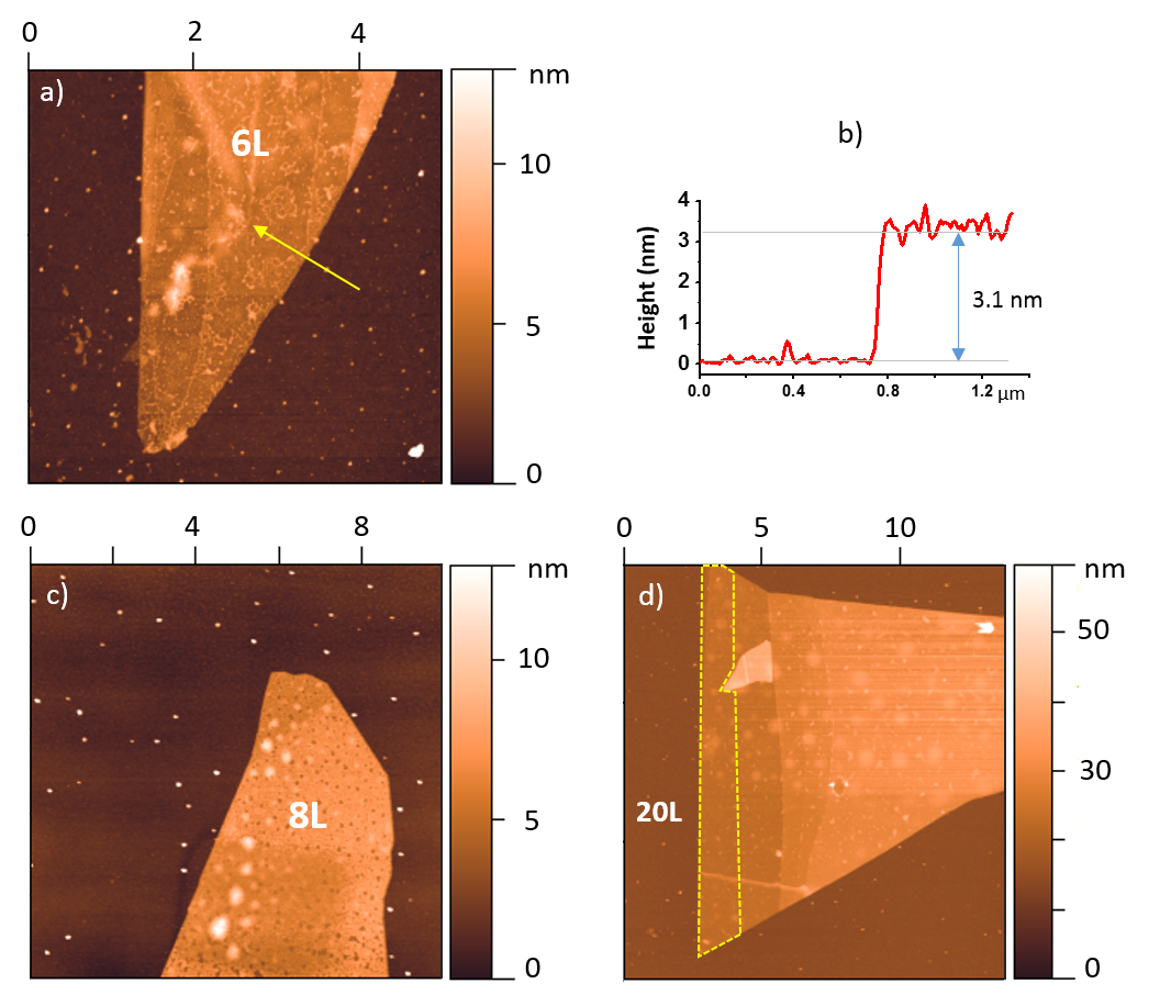
The BN sheets studied in this paper were all exfoliated from Saint-Gobain crystallites. Mechanical peeling was used following the method initially developed for graphene.Novoselov et al. (2004) The powder is applied to an adhesive tape, whose repeated folding and peeling apart separates the layers. They are further transferred onto a Si wafer covered with 90 nm of SiO2, the optimal thickness for imaging BN flakes with a maximal optical contrast. Gorbachev et al. (2011) The SiO2/Si substrates are also covered with a network of Cr/Au finder marks deposited by UV lithography with the AZ5214E photoresist and Joule evaporation in order to facilitate the localization of the flakes. Prior to the layer transfer, the wafer was chemically cleaned with acetone and isopropanol, followed by several minutes of exposure to a O2 plasma (60W, P12 nbar). The last step of this preparation renders the SiO2 surface hydrophilic and more sensitive to water contamination. That is the reason why we prefer to use the optical contrast (OC) for thickness determination after a Atomic Force Microscopy (AFM) calibration procedure on folded parts (see description in Supporting Information).
The optical properties of BN samples were analyzed by cathodoluminescence using an optical system (Horiba Jobin Yvon SA) installed on a JEOL7001F field-emission gun scanning electron microscope (SEM). The samples are mounted on a GATAN cryostat SEM-stage cooled down to 5 K with a continuous flow of liquid helium. The samples are excited by electrons accelerated at 2 kV with a beam current of 1 nA. Exfoliated layers were measured using either a fixed electron beam excitation, or for the thinnest flakes, a fast e-beam scanning on the sample in order to limit e-beam-induced modifications. The CL emission is collected by a parabolic mirror and focused with mirror optics on the entrance slit of a 55 cm-focal length monochromator. The all-mirror optics combined with a suited choice of UV detectors and gratings ensures a high spectral sensitivity down to 190 nm. A silicon charge-coupled-display (CCD) camera is used to record the spectra. The spectral response of the optical detection setup was measured from 200 to 400 nm using a deuterium lamp (LOT Oriel - Deuterium lamp DO544J - 30W) of calibrated spectral irradiance. The system response for each detector/grating combination was then obtained following the procedure described in Ref.30. All spectra reported in this paper are corrected from the system response. It was also checked that the CL linewidths are not limited by the spectral resolution of the apparatus (0.02 nm in the best conditions) excepted for the 6L flake acquisitions.
III Results
III.1 Intrinsic luminescence of bulk hBN
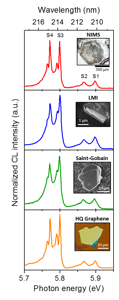
The CL spectra taken from the commercial samples (Saint-Gobain and HQ Graphene), the LMI sample and the reference crystal from NIMS are reported together in Fig. 1. Actually as these samples were synthesized using very different growth techniques whether it is concerning boron and nitrogen precursors, pressure or process temperature, they obviously cannot afford identical defects or impurities, which could act as trapping sites of the excitons. Pierret et al. (2014); Jaffrennou et al. (2007) Nevertheless, in spite of their differences, for all the samples, we observe a similar S series emission with the S1, S2, S3 and S4 lines emerging with a maximum at 5.898 eV (210.2 nm), 5.866 eV (211.4 nm), 5.797 eV (213.9 nm) and 5.771 eV (214.8 nm) respectively, as already reported in previous works. Watanabe and Taniguchi (2009); Cao et al. (2013); Pierret et al. (2014) This comparative study therefore strengthens the current interpretation attributing an intrinsic origin to the S lines. Jaffrennou et al. (2007); Watanabe and Taniguchi (2009)
According to this interpretation, the S emission lines observed in CL and PL have been assigned Jaffrennou et al. (2007); Watanabe and Taniguchi (2009) to the theoretical excitons calculated by Arnaud and Wirtz. Arnaud et al. (2006, 2008); Wirtz et al. (2006, 2008); Wirtz and Rubio (2009) Actually these calculations show that in the case of a perfect hexagonal symmetry, hBN present two doubly degenerate exciton levels, with a lower dark pair and an upper bright one. A symmetry lowering lifts the degeneracies so that four non degenerate levels are obtained. 111There are also dark triplet states which are not discussed here. It is not known precisely what is the reason for this symmetry lowering in our case: zero-point motionArnaud et al. (2008) or Jahn-Teller like effectWatanabe and Taniguchi (2009) have been suggested. In any case phonon effects and exciton-phonon couplings should be involved as indicated by the Stokes shift determined from the comparison of absorption measurements with the PL-CL spectra.Watanabe and Taniguchi (2011) It should be noticed that these interpretations assume that the main relevant absorption and luminescence processes are related to direct transitions although ab initio calculations predict an indirect gap between points in the Brillouin zone close to the K (and H) point for the valence and and close to the M (and L) point for the conduction band. One- or multiphonon processes should perhaps be taken into account.222G. Cassabois, P. Valvin and B. Gil, arXiv:1512.02962 [cond-mat.mtrl-sci]
Finally it is worth mentioning that the excitons described here present similarities with those observed in lamellar transition metal dichalcogenides (TMDs) in which case spin-orbit splitting is clearly observed. Qiu et al. (2013); Xu et al. (2013); Berghäuser and Malic (2014); Zhang and Zunger (2015) However the spin-orbit splitting should be very weak here for the light B and N elements. Looking at the spectra in more detail, the S3 and S4 emissions exhibit a fine structure splitting with a doublet separated by a few meV and assigned to the transverse and longitudinal components of exciton recombinations, as suggested by polarized-PL experiments.Watanabe and Taniguchi (2009) The S3 and S4 doublets are observed leading to the two S4 peaks at 5.762 eV and 5.768 eV and the two S3 peaks at 5.787 eV and 5.794 eV. They can be distinguished in the LMI and the Saint-Gobain powder samples but are better seen in the HQ and the NIMS crystals, the latter generally exhibiting narrower linewidths. We believe that this is due to the fact that the HQ and the NIMS samples were cooler, because mounted on a copper plate, than the two other ones, mounted on SiO2/Si substrates of lower thermal conductivity. Indeed, the S peak linewidths have been shown to be strongly dependent on the crystal temperature.Watanabe and Taniguchi (2009)
III.2 Thickness and luminescence of hBN flakes
Several examples of exfoliated flakes are presented in Fig. 2 and in Supplementary Information. The uncommon geometry of the exfoliated flake shown in Fig. 2 offers a good configuration to trace the luminescence properties as a function of the hBN thickness in the nanometer range. It displays three atomically-flat regions of 9, 20 and 32 nm thickness as deduced from the AFM profile (Fig. 2b). Assuming a hBN interplanar distance of 0.34 nm and a 1 nm water layer thickness, we estimate that the exfoliated sample is composed of 27, 60 and 100 layers respectively. It is important to notice that the contour outline of the flake is well-defined, suggesting that the hBN crystal is free of any glide defect, which is also confirmed by the absence of the D emission series in the CL spectra.Pierret et al. (2014); Watanabe and Taniguchi (2009) This strongly suggests the pristine AA’ stacking of hBN in these three thicknesses. The thickness steps are probably produced by a cleavage perpendicular to the basal plane during the tape removal. Planes with lowest indices (10.0) and (11.0) being the easier to split, the parallel step edges are thus probably oriented along the [11.0] and [10.0] directions respectively in the basal plane corresponding to armchair and zigzag edges respectively. Actually, a recent study reported a statistic of the edges structure in hBN exfoliated flakes and showed a slight preference for zigzag-type edges.Kim et al. (2011)
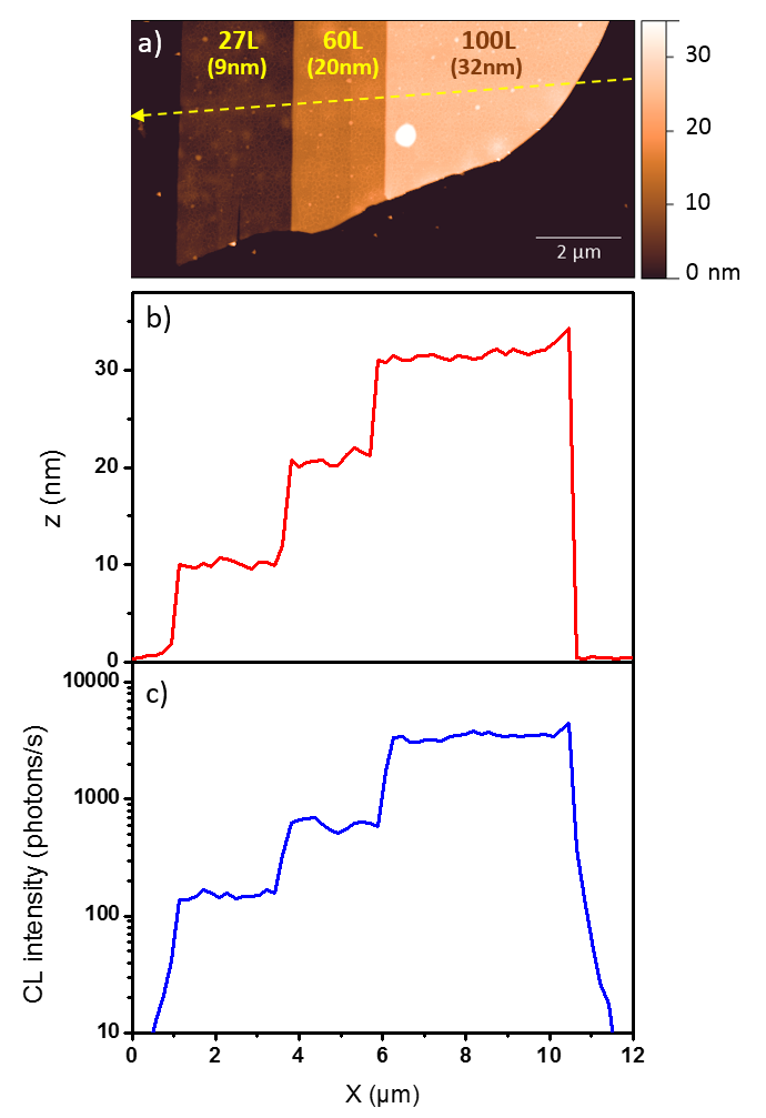
A CL linescan recorded perpendicularly to the step edges is reported in Fig. 2c. The CL intensity clearly decreases when reducing the hBN thickness. Such a result is expected because the electron-hole generation rate decreases with the thickness, thin flakes being almost transparent to the electron beam. However, it is remarkable that we obtain an almost homogeneous intensity of S emissions for a given thickness, also consistent with the integrity of the hBN crystal after exfoliation.
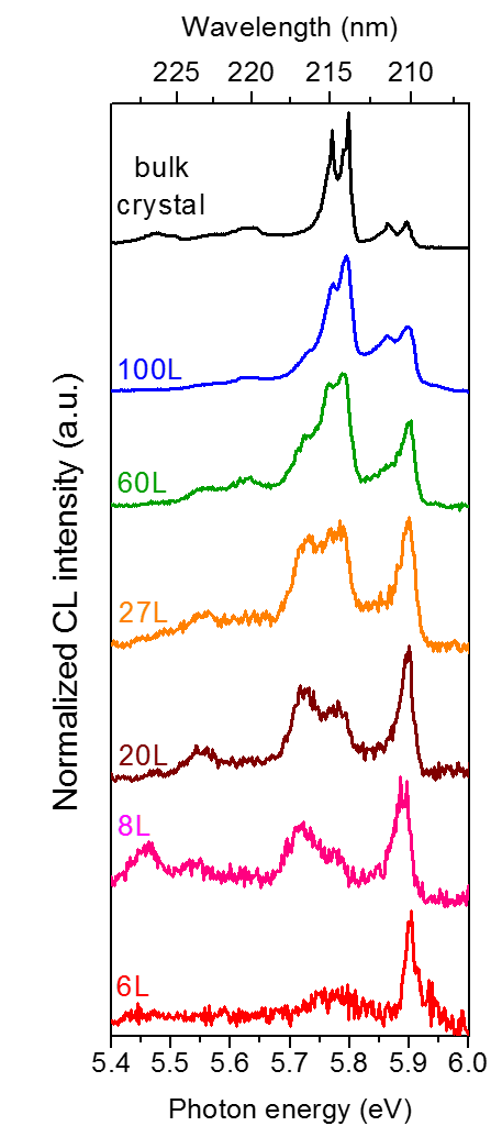
We stress here that we managed to isolate hBN layers free of exfoliation defects, which was not the case in our previous work. Pierret et al. (2014) It is attested by the CL spectra being now all dominated by the S exciton recombinations. The trend extracted from the defect-free Saint-Gobain flakes is summarized in Fig. 3 showing the CL spectra for thicknesses ranging from 100L to 6L. The spectrum of the bulk Saint-Gobain crystallite is also plotted for comparison. Strong modifications in the CL spectra appear within the 5.6-6 eV energy range for exfoliated layers. When reducing the thickness, one can see a significant decrease of the relative intensities of the S4, S3 and S2 lines compared to the S1 line. At the level of a few monolayers, it is remarkable that the characteristic S4, S3 and S2 lines of bulk hBN almost completely vanished.
This low dimensionality effect is not sample dependent and was in particular confirmed with hBN flakes exfoliated from the NIMS sample (see SFig.2 of the Supporting Information) leading to the conclusion that the observed thickness dependence is not governed by defect generation but has rather an intrinsic behavior. The S1 emission, which dominates the luminescence spectra of hBN flakes thinner than 20L, remains particularly sharp. The FWHM of this peak for the 6L sample is (17meV-0.6nm) which corresponds to the spectral resolution of the used experimental conditions. Besides, we observed a small energy shift of the S1 line from 5.871 eV for the bulk to 5.909 eV for the thinnest 6L flake. This shift could be a first indication of a modification in the intrinsic exciton emission energy such as a change in bandgap and/or in exciton binding energy. A similar interpretation has been proposed in a recent study wherein this singular emission at 5.9eV was observed in large-diameter BNNTs (60nm).Du et al. (2014)
IV Discussion
The only available ab initio study comparing bulk hBN and monolayer properties modeled the effect of varying the interplane distance.Wirtz et al. (2006) The calculated absorption spectra including excitonic effects shows that the bandgap increases with confinement, but the exciton binding energy also does in the same proportion, so that absorption peaks are expected to be in the same range of energy for the bulk and the monolayer ( eV). Given the uncertainty of such calculations, they appear consistent with our observations of a few tens of meV energy shifts of the S lines when reducing the number of layers of hBN.
Looking closer to the spectra for the 90L flake, a shoulder on the low energy side of the S4 peak can also be detected. For thinner samples, it emerges — together with the S1 line — as a broader peak of about 50 meV linewidth having a maximum at 5.726 eV (216.5 nm). This peak may be assigned to the LO phonon (169 meV) replica of the S1 line (5.898 eV). This assignment is strengthened by the observation of replica involving up to 3 phonons when using higher integration times (see Fig.S3 of the Supporting Information).
Flakes composed of less than 6L were also investigated in this work on SiO2/Si substrates but we have not yet succeeded in getting a significant CL signal in the 1-5 layers thickness range. Regarding the luminescence efficiency, the situation of BN on SiO2 is in contrast to that of suspended MoS2 layers where the quantum yield increases by a factor of 104 between 6L and 1L. For BN on SiO2, surface effects might hide a strong quantum yield increase as already pointed out in the first paper of Mak et al. on MoS2 monolayer Mak et al. (2010) and later further investigated by Buscema et al.Buscema et al. (2014) Non radiative surface states at the SiO2/BN interface or charge transfers to excitons could for instance hinder excitonic recombinations mechanism. Alternatively, the question rises whether a strong quantum yield increase could basically occur for the BN monolayer. Indeed, on the one hand, although some experiment led to propose a direct band gap, Watanabe et al. (2004) an indirect band gap is expected in the bulk from most theoretical calculations. On the other hand, bulk hBN is a strongly radiative material compared to other indirect gap materials. In fact, it is clear now that the electronic structure alone is not sufficient to explain hBN luminescence properties and that unusually strong excitonic effects are involved.
We now turn to the thickness dependent behavior of S lines. Actually, all ab initio calculations agree to predict for the monolayer a direct gap at points K, just as for di-chalcogenides,Blase et al. (1995); Wirtz and Rubio (2009); Ribeiro and Peres (2011); Berseneva et al. (2013) but the situation is simpler here since only two bands, the valence band and the conduction band have to be considered. As a consequence the lowest excitonic state is a double degenerate state (dark triplet states are not considered here) with a large binding energy about 2 eV.Wirtz et al. (2006) Within a semi-quantitative 2D Wannier-Mott model (k.p approximation) the Bohr radius is found about 8Å, Cao et al. (2013) which agrees with a more accurate tight-binding model. 333F. Ducastelle, 2015, unpublished The excitonic wave function has a typical triangular symmetry: if the hole is fixed on a nitrogen atom, the electronic density is centered on the neighboring boron atoms, just as in the bulk. Arnaud et al. (2006, 2008); Wirtz et al. (2008)
Moreover, the exciton in bulk hBN is extremely compact: the electron-hole pair extends over a few lattice parameters in the basal plane, but has an extremely limited extension over adjacent surrounding planes. That is the reason why the local structure of this exciton is not expected to be dramaticaly perturbed when stacking hBN planes. In some sense we can consider that it behaves as a Frenkel exciton along the stacking axis with a weak probability to jump from one plane to the other. In the case of hBN with the usual AA’ stacking where boron atoms are above nitrogen atoms and conversely, the two types of planes are really “optically” different and as confirmed by a simple tight-binding analysis, we expect a so-called Davydov splitting of the single layer exciton.Toyozawa (2003) Hence the two 2-fold excitons found in the ab initio calculations, a dark one and a bright one. As pointed out previously, the further (Jahn-Teller or Peierls-like) splitting of these states into four states and the corresponding induced oscillator strengths are certainly related to exciton-phonon interactions but the precise mechanism is still unknown. So to summarize, a single excitonic line is expected for the monolayer which gets splitted into four lines in the bulk hBN.
In any case our experiments seem to indicate that when decreasing the number of layers we tend to the situation where we observe the expected luminescence of a single layer with a single S level. Since we have not been able to observe luminescence below 6L — characterization of self-standing flakes is still under progress — this is not easy to interpret. One possibility just mentioned above is that the effective thickness for luminescence processes is reduced by a dead-layer effect produced by the SiO2 substrate interaction. Another one could be that the distortions and the symmetry lowering occurring in the bulk are no longer stable when decreasing the number of layers. Moreover, the idea that the monolayer exciton luminescence manifests itself from 100L and becomes dominant for hBN flakes below 20L could be explained by various approaches which have not been addressed for other 2D materials yet.
In conclusion, intrinsic luminescence of both bulk and exfoliated layers was identified as a function of the number of layers. Inspection of bulk crystals from several sources confirm that the intrinsic excitonic luminescence is composed of four main lines, the S lines, whereas for BN hexagonal layers it strongly depends on the number of layers and tends towards the theoretically expected behavior of a single layer due to the direct recombination of a free bright exciton. This thickness dependent behavior provides an unprecedented spectroscopic characterization of BN layers from the bulk down to a few layers. Exciton-phonons interactions would remain to study. Finally it shows that the detailed excitonic properties of bulk hBN or multilayers depend on the stacking sequences. This work confirms that h-BN displays unique properties within the family of layered semiconductors and paves the way towards future experimental and theoretical investigations of these properties .
Acknowledgements.
Catherine Journet-Gautier and Berangère Toury-Pierre, from LMI, are warmly acknowledged for providing one of their PDCs samples. Authors thank T. Taniguchi and K. Watanabe from NIMS for providing us a reference HPHT crystal, F. Withers from Manchester University for single, bi and tri-layer hBN samples, C. Vilar for technical help on cathodoluminescence-SEM setup, F. Fossard for helpful discussions, and Ch. Voisin for a careful reading of the manuscript. The research leading to these results has received funding from the European Union Seventh Framework Programme under grant agreement no. 604391 Graphene Flagship. We acknowledge funding by the French National Research Agency through Project No. ANR-14-CE08-0018.References
- Ju et al. (2014) L. Ju, J. Velasco, E. Huang, S. Kahn, C. Nosiglia, H.-Z. Tsai, W. Yang, T. Taniguchi, K. Watanabe, Y. Zhang, G. Zhang, M. Crommie, A. Zettl, and F. Wang, Nature nanotechnology 9, 348 (2014).
- Woods et al. (2014) C. R. Woods, L. Britnell, A. Eckmann, R. S. Ma, J. C. Lu, H. M. Guo, X. Lin, G. L. Yu, Y. Cao, R. V. Gorbachev, A. V. Kretinin, J. Park, L. A. Ponomarenko, M. I. Katsnelson, Y. N. Gornostyrev, K. Watanabe, T. Taniguchi, C. Casiraghi, H.-J. Gao, a. K. Geim, and K. S. Novoselov, Nature Physics 10, 451 (2014).
- Dean et al. (2010) C. R. Dean, A. F. Young, I. Meric, C. Lee, L. Wang, S. Sorgenfrei, K. Watanabe, T. Taniguchi, P. Kim, K. L. Shepard, and J. Hone, Nature nanotechnology 5, 722 (2010).
- Wang et al. (2013) L. Wang, I. Meric, P. Y. Huang, Q. Gao, Y. Gao, H. Tran, T. Taniguchi, K. Watanabe, L. M. Campos, D. A. Muller, J. Guo, P. Kim, J. Hone, K. L. Shepard, and C. R. Dean, Science 342, 614 (2013).
- Mishchenko et al. (2014) A. Mishchenko, J. S. Tu, Y. Cao, R. V. Gorbachev, J. R. Wallbank, M. T. Greenaway, V. E. Morozov, S. V. Morozov, M. J. Zhu, S. L. Wong, F. Withers, C. R. Woods, Y.-J. Kim, K. Watanabe, T. Taniguchi, E. E. Vdovin, O. Makarovsky, T. M. Fromhold, V. I. Fal’ko, A. K. Geim, L. Eaves, and K. S. Novoselov, Nature Nanotechnology , 1 (2014).
- Yankowitz et al. (2012) M. Yankowitz, J. Xue, D. Cormode, J. D. Sanchez-Yamagishi, K. Watanabe, T. Taniguchi, P. Jarillo-Herrero, P. Jacquod, and B. J. LeRoy, Nature Physics 8, 382 (2012).
- Yang et al. (2013) W. Yang, G. Chen, Z. Shi, C.-C. Liu, L. Zhang, G. Xie, M. Cheng, D. Wang, R. Yang, D. Shi, K. Watanabe, T. Taniguchi, Y. Yao, Y. Zhang, and G. Zhang, Nature materials 12, 792 (2013).
- Watanabe et al. (2004) K. Watanabe, T. Taniguchi, and H. Kanda, Nature materials 3, 404 (2004).
- Watanabe et al. (2006a) K. Watanabe, T. Taniguchi, T. Kuroda, and H. Kanda, Diamond and Related Materials 15, 1891 (2006a).
- Watanabe et al. (2006b) K. Watanabe, T. Taniguchi, T. Kuroda, and H. Kanda, Applied Physics Letters 89, 141902 (2006b).
- Silly et al. (2007) M. Silly, P. Jaffrennou, J. Barjon, J.-S. Lauret, F. Ducastelle, A. Loiseau, E. Obraztsova, B. Attal-Tretout, and E. Rosencher, Physical Review B 75, 085205 (2007).
- Jaffrennou et al. (2008) P. Jaffrennou, J. Barjon, T. Schmid, L. Museur, A. Kanaev, J.-S. Lauret, C. Zhi, C. Tang, Y. Bando, D. Golberg, B. Attal-Tretout, F. Ducastelle, and A. Loiseau, Physical Review B 77, 235422 (2008).
- Pierret et al. (2014) A. Pierret, J. Loayza, B. Berini, A. Betz, B. Plaçais, F. Ducastelle, J. Barjon, and A. Loiseau, Physical Review B 89, 035414 (2014).
- Pierret et al. (2015) A. Pierret, H. Nong, F. Fossard, B. Attal-Tretout, Y. Xue, D. Golberg, J. Barjon, and A. Loiseau, J. Appl. Phys. 118, 234307 (2015).
- Jaffrennou et al. (2007) P. Jaffrennou, J. Barjon, J.-S. Lauret, A. Loiseau, F. Ducastelle, and B. Attal-Tretout, Journal of Applied Physics 102, 116102 (2007).
- Watanabe and Taniguchi (2009) K. Watanabe and T. Taniguchi, Physical Review B 79, 193104 (2009).
- Mak et al. (2010) K. F. Mak, C. Lee, J. Hone, J. Shan, and T. F. Heinz, Physical Review Letters 105, 136805 (2010).
- Qiu et al. (2013) D. Y. Qiu, F. H. da Jornada, and S. G. Louie, Physical Review Letters 111, 216805 (2013).
- Zhao et al. (2012) W. Zhao, Z. Ghorannevis, L. Chu, M. Toh, C. Kloc, P.-H. Tan, and G. Eda, ACS nano 7, 791 (2012).
- Arnaud et al. (2006) B. Arnaud, S. Lebègue, P. Rabiller, and M. Alouani, Physical Review Letters 96, 026402 (2006).
- Arnaud et al. (2008) B. Arnaud, S. Lebègue, P. Rabiller, and M. Alouani, Phys. Rev. Lett. 100, 189702 (2008).
- Wirtz et al. (2005) L. Wirtz, A. Marini, M. Grüning, and A. Rubio, (2005), arXiv:cond-mat/0508421 [cond-mat] .
- Wirtz et al. (2006) L. Wirtz, A. Marini, and A. Rubio, Physical Review Letters 96, 126104 (2006).
- Wirtz et al. (2008) L. Wirtz, A. Marini, M. Grüning, C. Attaccalite, G. Kresse, and A. Rubio, Phys. Rev. Lett. 100, 189701 (2008).
- Yuan et al. (2014a) S. Yuan, B. Toury, C. Journet, and A. Brioude, Nanoscale 6, 7838 (2014a).
- Yuan et al. (2014b) S. Yuan, B. Toury, S. Benayoun, R. Chiriac, F. Gombault, C. Journet, and A. Brioude, European Journal of Inorganic Chemistry 2014, 5507 (2014b).
- Taniguchi and Watanabe (2007) T. Taniguchi and K. Watanabe, Journal of Crystal Growth 303, 525 (2007).
- Novoselov et al. (2004) K. S. Novoselov, A. K. Geim, S. V. Morozov, D. Jiang, Y. Zhang, S. V. Dubonos, I. V. Grigorieva, and A. A. Firsov, Science 306, 666 (2004).
- Gorbachev et al. (2011) R. V. Gorbachev, I. Riaz, R. R. Nair, R. Jalil, L. Britnell, B. D. Belle, E. W. Hill, K. S. Novoselov, K. Watanabe, T. Taniguchi, A. K. Geim, and P. Blake, Small 7, 465 (2011).
- Pagel et al. (2000) M. Pagel, V. Barbin, P. Blanc, and D. Ohnenstetter, Cathodoluminescence in Geosciences (Springer, 2000).
- Cao et al. (2013) X. K. Cao, B. Clubine, J. H. Edgar, J. Y. Lin, and H. X. Jiang, Applied Physics Letters 103, 191106 (2013).
- Wirtz and Rubio (2009) L. Wirtz and A. Rubio, in B-C-N Nanotubes and Related Nanostructures, Lecture Notes in Nanoscale Science and Technology, Vol. 6 (Springer New York, 2009) pp. 105–148.
- Note (1) There are also dark triplet states which are not discussed here.
- Watanabe and Taniguchi (2011) K. Watanabe and T. Taniguchi, Int. J. Appl. Ceram. Technol. 8, 977 (2011).
- Note (2) G. Cassabois, P. Valvin and B. Gil, arXiv:1512.02962 [cond-mat.mtrl-sci].
- Xu et al. (2013) M. Xu, T. Liang, M. Shi, and H. Chen, Chemical Reviews 113, 3766 (2013).
- Berghäuser and Malic (2014) G. Berghäuser and E. Malic, Phys. Rev. B 89, 125309 (2014).
- Zhang and Zunger (2015) L. Zhang and A. Zunger, Nano Letters 15, 949 (2015).
- Kim et al. (2011) J. S. Kim, K. B. Borisenko, V. Nicolosi, and A. I. Kirkland, ACS Nano 5, 3977 (2011).
- Du et al. (2014) X. Z. Du, C. D. Frye, J. H. Edgar, J. Y. Lin, and H. X. Jiang, J. Appl. Phys. 115, 053503 (2014).
- Buscema et al. (2014) M. Buscema, G. A. Steele, H. S. J. van der Zant, and A. Castellanos-Gomez, Nano Res. 7, 1 (2014).
- Blase et al. (1995) X. Blase, A. Rubio, S. G. Louie, and M. L. Cohen, Phys. Rev. B 51, 6868 (1995).
- Ribeiro and Peres (2011) R. M. Ribeiro and N. M. R. Peres, Phys. Rev. B 83, 235312 (2011).
- Berseneva et al. (2013) N. Berseneva, A. Gulans, A. V. Krasheninnikov, and R. M. Nieminen, Phys. Rev. B 87, 035404 (2013).
- Note (3) F. Ducastelle, 2015, unpublished.
- Toyozawa (2003) Y. Toyozawa, Optical Processes in Solids (Cambridge University Press, 2003).
- Blake et al. (2007) P. Blake, E. W. Hill, A. H. Castro Neto, K. S. Novoselov, D. Jiang, R. Yang, T. J. Booth, and A. K. Geim, Applied Physics Letters 91, 063124 (2007), http://dx.doi.org/10.1063/1.2768624.
- Wirtz et al. (2003) L. Wirtz, A. Rubio, R. A. de la Concha, and A. Loiseau, Phys. Rev. B 68, 045425 (2003).
Supplementary Information
Calibration of thickness measurement
As pointed out in the main body of the text, due to the hydrophilic character of the SiO2 surface, it tends to absorb water and results in a typically 1 nm-thick water layer captured between SiO2 and BN. As for graphene, this complicates the thickness measurements of atomically-thin BN flakes by the AFM technique. Indeed we have observed that the water layer thickness is relatively inhomogeneous over the wafer, which induces a strong inaccuracy in determining the thickness of few-monolayer flakes by AFM. Thickness measurement by optical contrast (OC) imaging under visible light illumination is then preferred in this work, because it appears to be less perturbed by the presence of water. By using Differential Interference Contrast microscopy (DIC), the OC was first calibrated with AFM measurements specifically taken on BN flakes having folded parts. This ensures the step height between the folded part and the unfolded one, to be independent on the amount of water trapped between hBN and SiO2.
To that end, a Dimension 3100 scanning probe microscope from Brukers company equipped with commercial MPP11-100 AFM tips was used in tapping mode. The OC was measured with the same parameters (filters, exposure time) for two folded flakes deposited onto the SiO2/Si substrate as shown in SFig.1a and SFig.1b. The values are plotted as a function of the number of layer measured by AFM in SFig.1c. We observe a linear dependence of the OC on the hBN thickness up to 20L, with approximately 1.5% of contrast per layer in good agreement with the literatureGorbachev et al. (2011) much lower than the % OC of graphene.Blake et al. (2007) It is remarkable that the OC line crosses the axis at 0L, which confirms the small dependence of OC-based thickness measurements on the presence of water. Considering the small thickness of the water layer (1nm) compared to the SiO2 thickness (90 nm) and the small refractive index difference between SiO2 (1.45) and water (1.33) compared to hBN (1.8), the contrast measurement appears to be robust upon water contamination and allows a more accurate thickness determination than AFM for hBN thicknesses below 20L-6 nm.
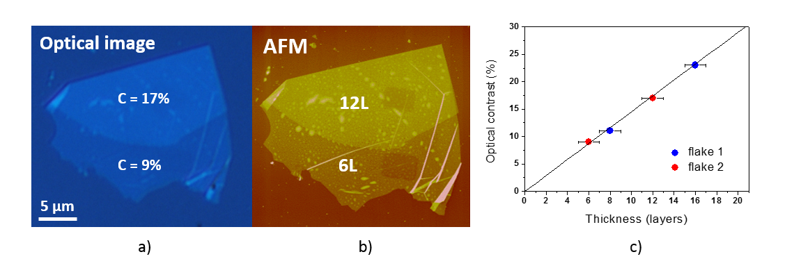
The low-dimensionality effect is not sample-dependent
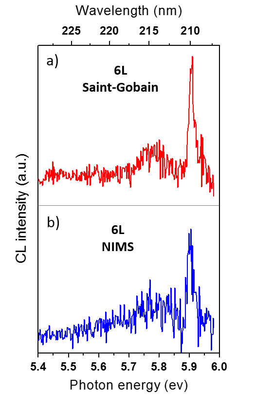
Phonon replicas
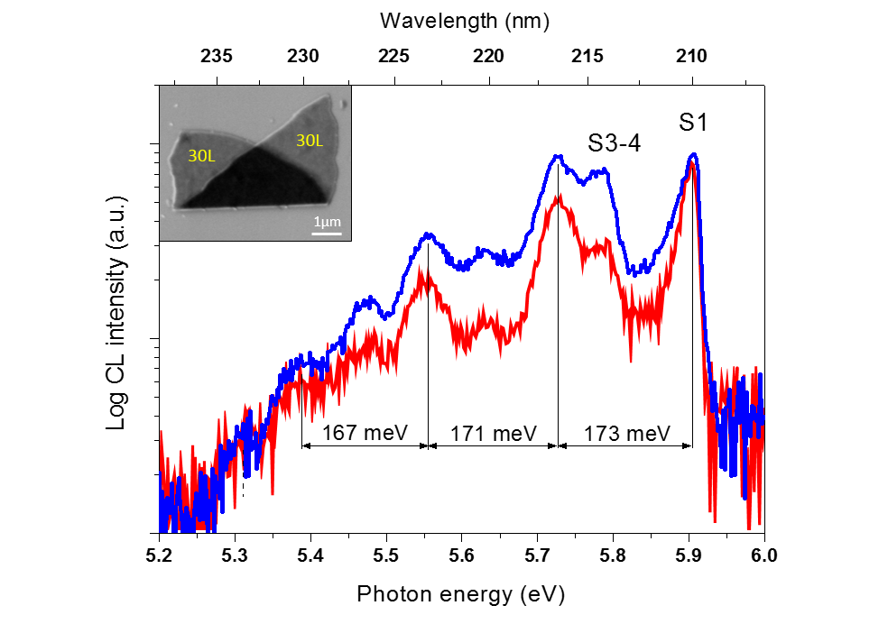
Recorded using higher exposure time, the CL spectra of SFig. 3 exhibit lower energy replicas of S1 and S3-4 lines. Associated with the S1 emission at 5.903eV, we detect peaks at 5.730eV, 5.559eV and 5.392eV with decreasing intensities. The peaks are shifted by a constant energy value of 171 meV. This energy almost exactly corresponds to the 169 meV energy of the LO phonon (Raman-active) mode E2g of hBN. This mode is related to in-plane vibrations that is the reason why the number of hBN layers does not affect significantly its energy as shown experimentallyGorbachev et al. (2011) and theoretically.Wirtz et al. (2003) In SFig. 3, we also observe the phonon replicas of the S3-4 lines already reported in our previous study.Pierret et al. (2014)
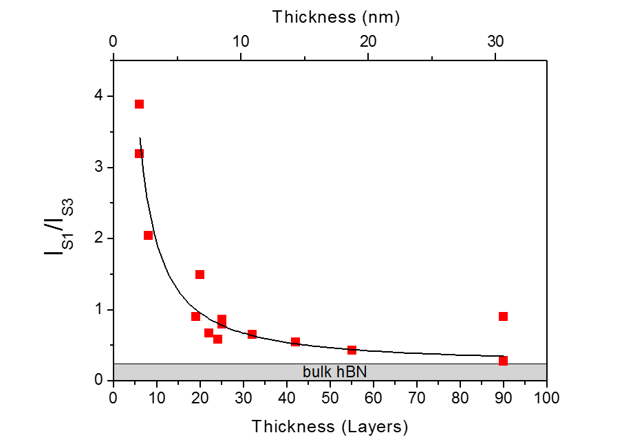
Relative intensities of S lines as a function of the thickness
In SFig. 4 we plot the intensity ratio between S1 and S3 luminescence intensities for several exfoliated hBN flakes with various thicknesses. One can easily note the increasing value of the S1/S3 ratio when reducing hBN thickness. According to our interpretation the S1 line is probably related to the single sheet exciton which can be considered as a surface contribution, while the S3 line appears as a characteristic of bulk hBN. Hence, the ratio is expected to be strongly dependent on the surface/volume ratio (1/d). Then, the fit was obtained by using the expression where is a fixed parameter whose value is systematically measured for submicrometric hBN samples. We found that the best fit is obtained for . Finding a value of close to 1 is in a good agreement with the surface origin of the S1 peak.
AFM characterization of thin hBN flakes
