Plasmon Excitations for Encapsulated Graphene
Abstract
We have developed an analytical formulation to calculate the plasmon dispersion relation for a two-dimensional layer which is encapsulated within a narrow spatial gap between two bulk half-space plasmas. This is based on a solution of the inverse dielectric function integral equation within the random-phase approximation (RPA). We take into account the nonlocality of the plasmon dispersion relation for both gapped and gapless graphene as the sandwiched two-dimensional (2D) semiconductor plasma. The associated nonlocal graphene plasmon spectrum coupled to the “sandwich” system is exhibited in density plots, which show a linear mode and a pair of depolarization modes shifted from the bulk plasma frequency.
pacs:
73.21.-b, 71.70.Ej, 73.20.Mf, 71.45.Gm, 71.10.Ca, 81.05.ueI Introduction
The properties of high-quality graphene encapsulated between two films such as hexagonal boron-nitride are just beginning to be explored and have now become an active area of research due to recent advances in device fabrication techniques encaps1 ; encaps2 ; encaps3 ; encaps4 ; encaps5 ; encaps6 ; encaps7 ; encaps8 ; encaps9 ; encaps10 . Interest in the optical properties of these heterostructures has been focused on their unusual plasmonic behavior including their spatial dispersion and damping. This hybrid system may be employed for tailoring novel metamaterials. Additionally, this fabrication technique provides a clean environment for graphene. This brand new area of nanoscience not only poses challenges for experimentalists, but also for theoreticians seeking to formulate a theory for a model system. Although there already exists a copious literature on graphene on a single substrate GG ; ONB ; NJMH ; Pol1 ; Pol2 ; Pol3 ; Pol4 ; Pol5 , this study shows that encapsulated graphene is vastly different in many ways.
The model we use in this paper consists of two identical semi-infinite metallic plasmas with planar boundaries at . Within the spatial separation between the two bulk conducting plasmas () is inserted a 2D monolayer graphene sheet at , shown schematically in Fig. 1. The natural first step in our calculations of the plasmon excitation spectrum is to set up and solve the random-phase approximation (RPA) integral equation for the inverse dielectric screening function of this hybrid system. We have solved this equation analytically in position representation for a narrow spatial gap between the bulk half-space plasmas, obtaining a closed-form formula for the inverse dielectric function in terms of the nonlocal polarizability for graphene and the bulk metallic polarizability, for which the latter is well approximated by the hydrodynamical model. Based on this newly derived formula, we have calculated the nonlocal plasmon dispersion relation numerically, considering both gapped and gapless graphene as the two-dimensional (2D) semiconductor plasma. The resulting nonlocal graphene plasmon spectra coupled to the “sandwich” system are exhibited in density plots, which show a linear mode and a pair of depolarization modes shifted from the bulk plasma frequency.
Hexagonal boron nitride has been the main substrate material that facilitates graphene based devices to exhibit micrometer-scale ballistic transport. The recent work of Kretinin, et al. encaps10 has shown that other atomically flat crystals may also be employed as substrates for making high-quality graphene heterostructures. Alternative substrates for encapsulating graphene include molybdenum and tungsten disulfides which have been found to exhibit consistently high carrier mobilities of about cm2 V-1 s-1. On the other hand, when graphene is encapsulated with atomically flat layered oxides such as mica, bismuth strontium calcium copper oxide, or vanadium pentoxide, the result is remarkably low quality graphene with mobilities of about cm2 V-1 s-1. This difference is due mainly to self-cleansing which occurs at interfaces between graphene, hexagonal boron nitride, and transition metal dichalcogenides. In our model calculations, we allow for the possibility that the substrate may affect the energy band structure of graphene by opening a gap in the energy band. We compare the resulting calculated plasmon spectra for encapsulated gapless and gapped graphene.
The work of Chuang, et al. DD1 is a study of the graphene-like high mobility for p- and n-doped WSe2. Electron transport in the junction between two 2D materials and graphene have also been reported recently, showing how spatial confinement can influence physical properties DD2 . Mobility, transconductance and carrier inhomogeniety experiments have also been reported in DD3 ; DD4 ; DD5 ; DD6 for monolayer and bilayer graphene fabricated on hexagonal BN as well as mica based substrates.
The outline of the rest of our paper is as follows. In Sec. II, we give details of our calculation of the inverse dielectric function for a 2D layer sandwiched between two conducting substrates whose separation is very small. We explicitly derive the plasma dispersion equation when the thick substrate layers may be treated in the hydrodynamical model. The 2D RPA ring diagram polarization function for graphene at arbitrary temperature is employed in the dispersion equation. A careful determination of the plasmon spectra for a range of energy gap and carrier doping values is reported in Sec. III. We conclude with a discussion of the highlights of our calculations in Sec. IV.

II Theoretical Formulation
We consider two identical semi-infinite conductors on either side of a 2D semiconductor layer (Fig. 1). One of the conductors extends from to while the other conductor has its surface at and extends to . The 2D layer lies in a plane mid-way between the two conductors at in the gap region . The inverse dielectric function satisfies
| (1) | |||||
where is the bulk infinite space symmetric conducting medium inverse dielectric function and
| (2) |
which defines in terms of the 2D ring diagram . For a narrow gap between the two identical half-space slabs, i.e., , the gap polarizability is given by
| (3) |
| (4) |
Setting in the equation relating to above, we may solve for and then obtain
| (5) |
so that the plasma excitation frequencies are determined by solving for the zeros of
| (6) | |||||
Expressing Eq. (4) in terms of the Fourier transform of , we obtain
| (7) |
Using the hydrodynamical model for nonlocality of the conducting substrate EGUI ; Kamen , we have , where is the local bulk metallic plasma frequency, is an adjustable parameter which mabe adjusted to give the correct dispersive shift of the bulk plasma frequency, i.e., (where is the bulk Fermi velocity of the conducting substrate). This approximation leads to the dispersion equation which, after performing the integrations, we obtain
| (8) | |||||
where .
The 2D RPA ring diagram polarization function for graphene with a gap may be expressed as
III Numerical Results and Discussion
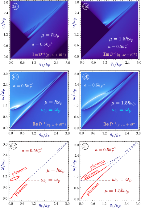
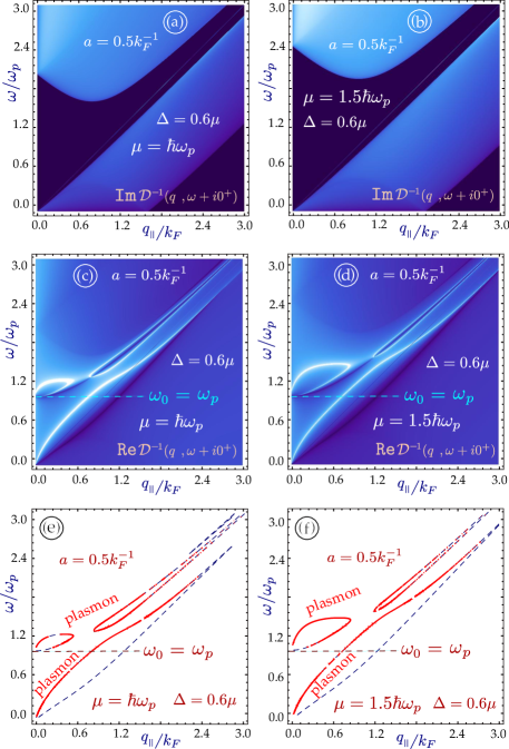
In the figures, we present calculated results for the nonlocal plasmon excitations of encapsulated gapless and gapped graphene. As we demonstrated in previous work GG ; ONB , the hybrid plasmon modes and their damping are mainly determined by the doping concentration, i.e., the chemical potential , along with the energy bandgap . Consequently, we have paid particular attention in our numerical investigations to the various regimes of the ratio . In Fig. 2, we exhibit results for gapless graphene. Figures 3 and 4 illustrate the case in which the graphene layer has an intermediate or large energy gap. The regions of strong damping arise from inter-band transitions which are forbidden by Pauli blocking (i.e., when the final transition states are filled, so that further transitions cannot occur). In the case of a single substrate and a 2D layer, the lowest acoustic branch vanishes due to damping in the long wavelength limit for a range of separations between the 2D layer and the surface. However, this is not the present case under consideration involving encapsulation of the graphene sheet within a small gap between the two surfaces. Within the “small gap” framework, , the lower branch is never damped in the long wavelength limit. This result is quite different from that obtained for a single substrate, in which strong damping of the acoustic branch appears in the long wavelength limit for the distance below a specific critical value. In regard to the two upper branches, attributed to bulk three-dimensional plasmons, their undamped parts appear as upper and lower arcs of a single loop on the left sides of the figures in the cases of low doping or low value of the chemical potential, as clearly demonstrated in Fig.2. It is noteworthy that both bulk plasmon modes start from , not from as we previously observed in the case of a single conducting substrate.
The presence of a bandgap in the graphene energy spectrum leads to interesting features. First, a finite energy gap modifies the location of each single-particle excitation region. It is especially unusual to observe the extension of the upper plasmon branches, which are understood to arise from a semi-infinite substrate. It is also apparent that the acoustic mode is broken into two separate undamped parts located between the two distinct single-particle excitation regions, as has been previously reported for free-standing gapped graphene pavlo (see Figs. 3 (c) and (d)). The figures show that specifically acoustic plasmon mode behavior persists in our present case of encapsulated graphene. Within the framework of our assumption that the spacing between the conducting half-spaces is narrow, , the results are relatively insensitive to the gap separation, and we consider only small values of . Moreover, we examined modification of the plasmon spectra for various values of the Fermi energy, , as depicted in Figs. 2 through 4.
In the matter of experimental realization of our results, it is necessary to achieve a situation in which the surface plasmons are not Landau damped, i.e., the corresponding branches are located outside of the upper inter-band part of the single-particle excitation spectrum. Accordingly, the frequency of the surface plasmon mode should be comparable with the Fermi energy in graphene, as well as with the corresponding -2D-graphene plasmon energy. Only if this condition is satisfied will it be possible to observe the strong plasmon coupling we have reported here. Therefore, one must ensure that the bulk plasmon frequency is in the range of and below NPo1 . Ref [NPo1, ] is an experimental paper on which is a heavily doped topological insulator, where the surface plasmon energy was found to be around . Evidence of mutual interaction between the surface plasmon and the Dirac plasmon of has been provided by using high-resolution electron energy loss spectroscopy. Additionally, at a graphene/ interface, which was recently experimentally realized by Kepaptsoglou, et al. NPo2 , the surface plasmon of is hybridized with acoustic plasmons in graphene. In this vein, the Fermi energy of free-standing graphene corresponding to an electron density is , so the two quantities are of the same order of magnitude.

IV Concluding Remarks
In this paper, we have investigated the properties of the plasmon spectra for a heterostructure consisting of a pair of identical semi-infinite conductors and a 2D graphene layer sandwiched between them. Our formulation is suitable when the separation between the two semi-infinite bulk conducting materials is small compared to the inverse Fermi wave number in graphene, and the whole system is symmetric in the direction perpendicular to the 2D layer.
We have obtained the plasmon dispersion relations for this encapsulated graphene system for both zero and finite energy bandgap and for various values of the chemical potential. In each case, we clearly obtain three hybridized plasmon modes, one of which (the acoustic branch) starts from the origin and is attributed primarily to the graphene layer and the other two modes originating at are considered as optical plasmons. This situation is novel and has not been encountered previously in a system involving a 2D layer with a single semi-infinite conductor. Each of the branches exhibits a specific behavior depending on the chemical potential and consists of various undamped parts which are determined by the energy bandgap and its ratio to the doping parameter, as discussed above.
The low-frequency branch has a linear dispersion at long wavelengths and becomes damped by the intra-band and inter-band particle-hole modes as wave vector is increased. There are two bulk plasmon branches which are depolarization shifted by the Coulomb interaction. In this regard, the results demonstrate that there is almost no dependence on the distance between the two substrates as long as the condition is satisfied. Moreover, there is no evidence of critical damping of the acoustic plasmon branch in the long wavelength limit (), as was found in the previous comparative study of a monolayer of graphene interacting with a single conducting substrate GG . Furthermore, some crucial properties of the plasmons in free-standing graphene with an energy bandgap, such as extension of the undamped branch and its separation into the two parts for intermediate energy gap , are also present in our results.
In summary, we have developed a new analytical model and obtained a complete set of numerical results for a two-dimensional layer (graphene) surrounded by two identical thick conducting substrates. While our previous work GG confirmed and offered an adequate theoretical explanation for recent experimental findings Pol1 ; Pol2 ; Pol3 ; Pol4 , this paper is expected to predict the correct plasmon behavior of the totally realistic and novel situation of encapsulated graphene, which is now being very actively studied experimentally Gong ; Kamat . Hybridized plasmon modes of a graphene-based nanoscale system are at the focus of significant interest in the current fields of technology and applications. The authors of encaps5 report evidence of the formation of electron-hole puddles for encapsulated graphene by hexagonal BN. This is an interesting effect which was not taken into account in our model calculations. These localization effects will be investigated in future work by including a concentration of impurities and defects in interaction with the 2D layer and two substrates. The role of impurities is expected to be modest at low concentration. An increase in the concentration of the impurities will lead to a decrease in the electron correlations. The Green’s function and consequently will, in this case, be expressible by vertex corrections by the usual rules of field theory when impurities are present.
References
- (1) Principi A., Carrega M., Lundeberg M. B., Woessner A., Koppens F. H. L., Vignale G., and Polini M.,“Plasmon losses due to electron-phonon scattering: The case of graphene encapsulated in hexagonal boron nitride,” Phys. Rev. B 90, 165408 (2014).
- (2) Kharche N. and Nayak S.K.,“Quasiparticle Band Gap Engineering of Graphene and Graphone on Hexagonal Boron Nitride Substrate,” Nano Lett. 11, 5274 (2011).
- (3) Ristein J., Mammadov S., and Seyller T,“Origin of Doping in Quasi-Free-Standing Graphene on Silicon Carbide,” Phys. Rev. Lett. 108, 246104 (2012).
- (4) Ryzhii V. and Satou A.,“Plasma waves in two-dimensional electron-hole system in gated graphene heterostructures,” Jour. Appl. Phys. 101, 024509 (2007).
- (5) Woessner A., Lundeberg M. B., Gao Y., Principi A., Gonz lez P.A., Carrega M., Watanabe K., Taniguchi T., Vignale G., Polini M., Hone J., Hillenbrand R., and Koppens F.H.L.,“Highly confined low-loss plasmons in graphene boron nitride heterostructures,” Nature Materials 14, 421 (2015).
- (6) Mayorov A. S., Gorbachev R. V., Morozov S.V., Britnell L., Jalil R., Ponomarenko L.A.,Blake B., Novoselov K.S., Watanabe K., Taniguchi T., and Geim A.K.,“Micrometer-Scale Ballistic Transport in Encapsulated Graphene at Room Temperature,” Nano Lett. 11 (6), 2396 (2011).
- (7) Guimar es M.H.D., Zomer P.J., Ingla-Ayn s J., Brant J.C., Tombros N., and Wees B.J.V.,“Controlling Spin Relaxation in Hexagonal BN-Encapsulated Graphene with a Transverse Electric Field,” Phys. Rev. Lett. 113 086602 (2014).
- (8) Yang S., Feng X., Ivanovici S.,and M llen K., “Fabrication of Graphene-Encapsulated Oxide Nanoparticles: Towards High-Performance Anode Materials for Lithium Storage,” Angewandte Chemie. 49, 8408 (2010).
- (9) Britnell L., Gorbachev R.V., Jalil R., Belle B.D., Schedin F., Mishchenko A., Georgiou T., Katsnelson M.I., Eaves L., Morozov5 S.V., Peres N.M.R., Leist J., Geim A.K, Novoselov K.S., Ponomarenko L.A.,“Field-Effect Tunneling Transistor Based on Vertical Graphene Heterostructures,” Science 335, 6071 (2012).
- (10) Kretinin A.V., Cao Y., Tu J.S., Yu G.L., Jalil R. , Novoselov K.S., Haigh S.J., Gholinia A., Mishchenko A., Lozada M., Georgiou T., Woods C.R., Withers F., Blake P., Eda g., Wirsig A., Hucho C., Watanabe K., Taniguchi T., Geim A.K., and Gorbachev R.V.,“Electronic Properties of Graphene Encapsulated with Different Two-Dimensional Atomic Crystals,” Nano Lett. 14 , 3270 (2014).
- (11) Gumbs G, Iurov A., and Horing N.J.M.,“Nonlocal plasma spectrum of graphene interacting with a thick conductor,” Phys. Rev. B91, 235416 (2015).
- (12) Horing N.J.M., Iurov A., Gumbs G., Politano A., Chiarello G.,“Recent Progress on Nonlocal Graphene/Surface Plasmons,” (pp. 205-237), Springer International Publishing (2016).
- (13) Horing N. J. M.,“Coupling of graphene and surface plasmons,” Phys. Rev. B80, 193401 (2009).
- (14) Politano A., Marino A.R., Formoso V., Far as D., Miranda R., and Chiarello G.,“Evidence for acoustic-like plasmons on epitaxial graphene on Pt(111),” Phys. Rev. B 84, 033401 (2011).
- (15) Politano A., Marino A. R., and Chiarello G.,“Effects of a humid environment on the sheet plasmon resonance in epitaxial graphene,” Phys. Rev. B 86, 085420 (2012).
- (16) Politano A., Formoso V., and Chiarello G.,“Evidence of composite plasmon phonon modes in the electronic response of epitaxial graphene,”, Journal of Physics: Condensed Matter, 25 (34), 345303 (2013).
- (17) Politano A. and Chiarello G.,“Quenching of plasmons modes in air-exposed graphene-Ru contacts for plasmonic devices ,”, Applied Physics Letters, 102 , 201608. (2013).
- (18) Politano A. and Chiarello G., “Unravelling suitable graphene metal contacts for graphene-based plasmonic devices,” Nanoscale, 5, 8215(2013).
- (19) Chuang H. J., Tan X., Ghimire N. J., Perera M. M., Chamlagain B., Cheng M. M. C., Yan J., Mandrus D., Tomanek D., and Zhou Z., “High Mobility WSe2 p- and n-Type Field-Effect Transistors Contacted by Highly Doped Graphene for Low-Resistance Contacts,” Nano Lett. 14 3594 3601 (2014).
- (20) Shih C.J., Wang Q. H. , Son Y., Jin Z., Blankschtein D., and Strano M. S., “Tuning On-Off Current Ration and Field-Effect Mobility in a Graphene Heterostructure via Schottky Barrier Modulation,” ACS Nano, 8, 5790 (2014).
- (21) Low C. G., Zhang Q., Hao Y., and Ruoff R. S.,“Graphene Field Effect Transistors with Mica as Gate Dielectric Layers,” Nano Small Micro, 10, 4213 ,(2014).
- (22) Kretinin A. V., Cao Y., Tu J. S., Yu G. L., Jalil R., Novoselov K. S. , Haigh S. J., Gholinia A., Mishchenko A., Lozada M., Georgiou T., Woods C. R., Withers F. , Blake P., Eda G., Wirsig A., Hucho C., Watanabe K., Taniguchi T., Geim A. K. , and Gorbachev R. V., “Electronic Properties of Graphene Encapsulated with Different Two-Dimensional Atomic Crystals,” Nano Lett. 14, 3270 (2014).
- (23) Sun T., Wang Z. L., Shi Z. J., Ran G. Z. , Xu W. J., Wang Z. Y. , Li Y. Z., Dai L., and Qin G. G.,“Multilayered graphene used as anode of organic light emitting devices,” Applied Phys. Lett. 96, 133301 (2010).
- (24) Dean C.R., Young A.F., Meric I., Lee C., Wang L., Sorgenfrei S. , Watanabe K., Taniguchi T., Kim P., Shepard K. L., and Hone J. “Boron nitride substrates for high quality graphene electron ics,” Nature Nanotechnology 5, 722 (2010).
- (25) Eguiluz, A. Ying S. C., and Quinn J. J., “Influence of the electron density profile on surface plasmons in a hydrodynamic model”, Phys. Rev. B 11, 2118 (1975).
- (26) Horing N. J. M., Kamen E. and, Gumbs G., “Surface correlation energy and the hydrodynamic model of dynamic, nonlocal bounded plasma response,” Phys. Rev. B 31, 8269 (1985).
- (27) Wunsch B., Stauber T., Sols F., and Guinea F.,“Dynamical polarization of graphene at finite doping,” New Jour. of Phys. 8, 318 (2006).
- (28) Pyatkovskiy P. K.,“Dynamical polarization, screening, and plasmons in gapped graphene,” J. Phys.: Condens. Matter 21, 025506 (2009).
- (29) Politano A., Silkin V.M., Nechaev I.A., Vitiello M.S., Viti L., Aliev Z.S., Babanly M.B., Chiarello G. , Echenique P.M., and Chulkov E.V.,“Interplay of Surface and Dirac Plasmons in Topological Insulators: The Case of ,” Phys. Rev. Lett. 115 216802 (2015) .
- (30) Kepaptsoglou D. M., Gilks D., Lari L., Ramasse Q. M., Galindo P., Weinert M., Li L., Nicotra G. and Lazarov V. K.,“STEM and EELS study of the Graphene Interface,” Microsc. Microanal. 21 1151 (2015).
- (31) Gong C., Hinojos D., Wang W., Nijem N., Shan B., Wallace R. M., Cho K., and Chabal Y. J.,“Metal Graphene Metal Sandwich Contacts for Enhanced Interface Bonding and Work Function Control” ACS Nano 6, 5381 5387 (2012).
- (32) Kamat P. V.,“Graphene-Based Nanoarchitectures. Anchoring Semiconductor and Metal Nanoparticles on a Two-Dimensional Carbon Support,” J. Phys. Chem. Lett., 1 (2), 520 527 (2010).