InAs nanowire with epitaxial aluminium as a single-electron transistor with fixed tunnel barriers
Abstract
We report on fabrication of single-electron transistors using InAs nanowires with epitaxial aluminium with fixed tunnel barriers made of aluminium oxide. The devices exhibit a hard superconducting gap induced by the proximized aluminium cover shell and they behave as metallic single-electron transistors. In contrast to the typical few channel contacts in semiconducting devices, our approach forms opaque multichannel contacts to a semiconducting wire and thus provides a complementary way to study them. In addition, we confirm that unwanted extra quantum dots can appear at the surface of the nanowire. Their presence is prevented in our devices, and also by inserting a protective layer of GaAs between the InAs and Al, the latter being suitable for standard measurement methods.
I Introduction
Semiconducting nanowires (NWs) are widely used nowadays in nanotechnology Samuelson et al. (2004); Thelander et al. (2006); Lieber and Wang (2007) as their transport properties can be easily tuned Doh et al. (2005); Liang et al. (2015). In particular, InAs NWs are of interest as they are optically active Li et al. (2006) and can act as a field-effect transistor Bryllert et al. (2006), a quantum dot Björk et al. (2004); van Dam et al. (2006); Sand-Jespersen et al. (2007); Lee et al. (2012); Chang et al. (2013); Lee et al. (2014) or a qubit (Nadj-Perge et al., 2010). Recently, the growth of a NW with a high quality interface between InAs and aluminium has been achieved Krogstrup et al. (2015), with a hard superconducting gap Chang et al. (2015), systems in which Majorana bound states have been observed Lutchyn et al. (2010); Oreg et al. (2010); Das et al. (2012); Albrecht et al. (2016). In these devices, the barriers are formed electrostatically to allow great flexibility of the barrier strength, contrary to “fixed” tunnel barriers one can find in metallic single-electron transistors (SETs). However the drawback of this flexibility is the limited number of open conductive channels Albrecht et al. (2016); Higginbotham et al. (2015) which can either limit the signal in case of large opacity of the barriers, or induce a leakage current in the other limit.
In this study, we present a simple device in an InAs NW proximized with epitaxial Al. The main idea is to use the aluminium shell on top of the InAs NW to form a fixed tunnel barrier, thus with InAs as a SET, as in a metallic system Fulton and Dolan (1987); Grabert and Devoret (1992). Compared to electrostatic tunnel barriers, aluminium oxide based tunnel contacts are known to possess superior properties: They have a large number of conduction channels, typically of the order of Averin and Pekola (2008); Maisi et al. (2011). It allows one to make them several orders of magnitude more opaque than the few channel contacts without losing in signal strength. The more opaque the tunnel junctions are, the better the approximation of sequential tunnelling is. Hence when probing the hardness of the superconducting gap, we observe consistently an order of magnitude lower leakage levels in the gap. For this reason, the combination of a metallic SET and a proximized InAs NW can give access to functionalities mixing SET and InAs NWs properties, not possible with standard techniques. In addition, our method reduces some technical difficulties: Only one gate per intentional QD is needed and it ensures good contacts between the NW and the external leads. It also prevents the appearance of parasitic effects due to the exposure of the InAs core during the fabrication process as the InAs core as well as the interface between InAs and Al remain intact. Such effects are prevented as well by inserting a protective layer between the InAs core and the Al layer. Several works already exist on the fabrication of a SET using semiconducting NWs with fixed tunnel barriers (i.e. not tunable by gate modulation), with, e.g., Si NWs Zhong et al. (2005); Hofheinz et al. (2006) or InAs/InP heterostructures Thelander et al. (2003).
II Fabrication
The hexagonal InAs NWs are grown by molecular beam epitaxy (MBE) using gold nanoparticles catalyst and are m long. The aluminium is then deposited epitaxially, covering entirely the NW, without breaking the vacuum to guarantee a good interface between InAs and Al Krogstrup et al. (2015). For some NWs, a buffer layer of GaAs, nm thick, is grown on top of the InAs, followed then by the Al deposition. These NWs form a stacking-fault free wurtzite phase, with misfit dislocations at the InAs/GaAs interface due to the 7% lattice mismatch, therefore the strain relaxes very quickly Popovitz-Biro et al. (2011). This intermediate GaAs layer is expected to reduce the stress at the surface of the InAs and improve the intrinsic properties of the NW (like e.g. carrier mobility), as already observed in various NWs with cover shells van Tilburg et al. (2010); Chia et al. (2012); Lin et al. (2013); Holloway et al. (2013); Ganjipour et al. (2014). A sketch of the cross section of the wires is shown Fig. 1(a). The devices with the GaAs covered shell are named “-GaAs”, and the others, with only the aluminium shell, are named “-Al”. We remind that the NWs with the GaAs layer also have an epitaxial layer of Al. We have a clean contact between the core and the Al layer which leads to a negligible energy barrier (i.e. no tunnel barrier is formed between the NW core and the superconducting layer) as shown previously Krogstrup et al. (2015); Chang et al. (2015).
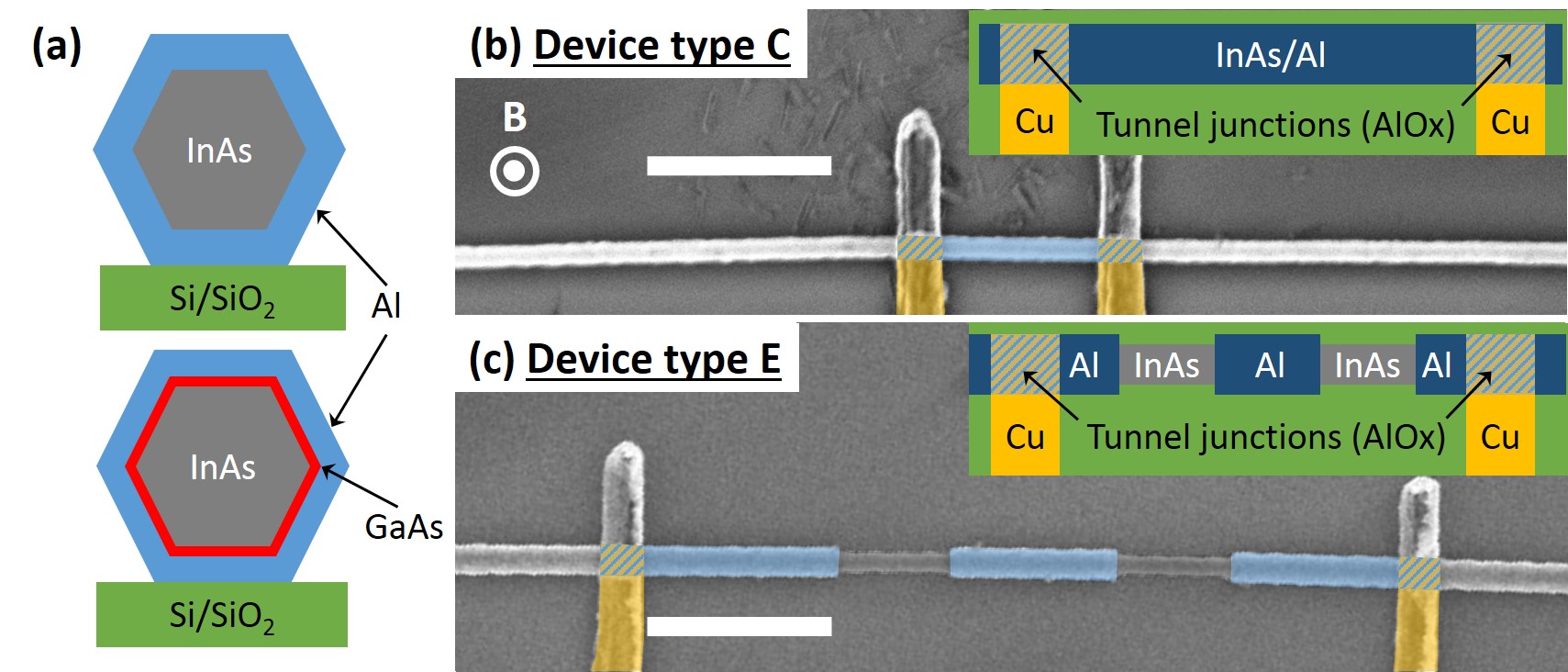
The NWs are transferred from the growth chip on a pre-marked substrate by dry deposition. The substrate is a highly-doped silicon wafer covered by 200 nm of silicon oxide and is used as a backgate. The position of the NWs is found on the chip using a scanning electron microscope (SEM). In order to study the effect of the chemical etching, we first isolate an Al island (m long) in the middle of the NW, by etching chemically at two places a 0.5 to 1 m segment of the Al shell by immersion in MF-CD-26 for 90 s at room temperature (called device “E”, for Etched). The remaining Al on the central island and on each side of the wire, close to the junctions, is supposed to keep the proximized superconductivity intact and uniform over the entire NW. The other type of devices is made without the chemical etching, keeping the aluminium shell intact and thus without any bare InAs (called device “C”, for Covered). The pre-marked chip is then covered with a resist and the two leads and the side gate are patterned by electron-beam lithography. After development, the pre-marked chip is inserted in an electron-beam evaporator equipped with a plasma gun. The native oxide layer on Al is removed by argon plasma etching inside the evaporator chamber. The epitaxial Al is then re-oxidised under O2 atmosphere of 2 mbar for 2 minutes to create the tunnel barriers, approximately 0.5 to 1 nm thick Gloos et al. (2003). 150 to 200 nm of Cu is next evaporated in order to make the leads and the side gate. The fact that the native Al oxide is etched in-situ ensures good control of the tunnel junctions. The tunnel barriers are expected only at the junctions and no barrier should form inside the NW. The junctions cover from 150 to 300 nm over the wire depending on the device and are spaced by 1 m (for the device C-Al’) and 5 m for the others. During the plasma etching and the oxygen re-oxidation, the InAs core is protected either by the Al shell where the junctions are made and by the resist everywhere else. Therefore we do not expect these treatments to damage further the InAs core. We emphasize that only Cu is deposited on the pre-marked chip, i.e. no Al layer is added: The tunnel junctions are formed by re-oxidizing the epitaxial Al layer grown from the MBE process after etching the native oxide layer. The sketches and SEM images of the devices are shown Figs. 1(b) and (c). The main parameters of the samples are given in Table 1. The NWs from the devices E-Al and C-Al come from the same growth, and the same applies for the devices E-GaAs and C-GaAs. The smaller resistance and charging energy of the device E-GaAs come from its wider tunnel junctions compared to the other devices. Only the backgate was used in this study, but we have obtained similar results using the side gate. All the measurements presented here have been performed in a dilution fridge at a bath temperature mK and, when applied, the magnetic field is perpendicular to the NW (see Fig. 1(b)). In the last section, conductance measurements have been performed, a lock-in amplifier was used with the excitation voltage ranging from to 10 V and the frequency from to 300 Hz depending on the gain and the bandwidth of the voltage and current amplifiers used.
According to Ref. Wunnicke (2006), the capacitance of the NW on the highly doped Si substrate is estimated to be fF for each device. We can then estimate the capacitance of the junctions supposing they cover half of a cylindrical NW (we cannot evaporate below the NW). In the case of aluminium oxide, we use the dielectric constant and the oxide thickness between 0.5 and 1 nm Gloos et al. (2003). We obtain thus the capacitance per junction fF, and thus the total capacitance fF, which gives the charging energy eV, close to the experiment. The total capacitance of the devices is mainly caused by the junctions, which are rather wide in our devices.
| Name | ||||||
| (eV) | (eV) | (nm) | (nm) | (nm) | ||
| E-Al | 180 k | 40a | 70 | 20 | n/a | |
| C-Al | 224 k | 202 | 45 | |||
| C-Al’ | 126 k | 192 | 30 | 40 | 20 | n/a |
| E-GaAs | 64 k | 195 | 10 | 50 | 25 | 5 |
| C-GaAs | 19 M | 195 | 65 |
a Taken at V
III Characterization of the devices
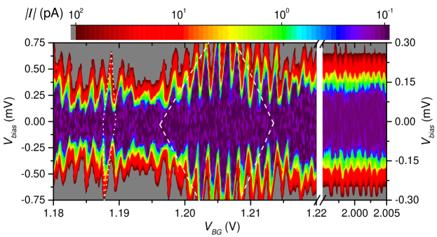
We first study the device E-Al, Fig. 1(c), in which the InAs core is exposed. Here, we choose the wire without GaAs, and etch Al in selected areas. The effect of the backgate on electron transport measurements is shown in Fig. 2. At negative backgate values (not shown), the transport is blocked. For V, a complex stability diagram is present, with at least two sets of Coulomb diamonds (see e.g. the white dotted and dashed diamonds in the left-hand side of Fig. 2). Only one QD is expected with a small charging energy. However, the QDs measured at intermediate gate values, around 1.2 V, show a charging energy between 0.3 and 0.8 meV, too high to reflect the main dot. These large values as well as the aperiodicity of the diamonds with are signatures of the presence of several QDs. Similar behaviour has been observed in several of our devices of the same type and unwanted QDs have as well been reported in previous study, despite the high quality of the NWs used Bleszynski et al. (2007); Boyd et al. (2011); Chang et al. (2015). It is believed to be caused by defects Schroer and Petta (2010) and potential fluctuations at the surface of the NW Weis et al. (2014) which can be triggered by chemical and/or plasma treatments of the NW. One reason for their presence comes from the fabrication process: The contacts on the NW are made directly on it, and in order to have an ohmic contact or to etch away a surface layer (the Al epitaxial layer in our case, see, e.g. the devices in Refs. Albrecht et al. (2016); Higginbotham et al. (2015)), additional chemical or plasma cleaning of the surface may be needed. These processes may deteriorate the surface of InAs, increasing thus the likelihood of forming unwanted QDs whose locations and sizes are not controlled. It is nevertheless possible to make them transparent by tuning locally its potential with additional side gates, leading to the fabrication of complex devices with potentially unnecessary side gates (see, e.g., some of the devices in Ref. Albrecht et al. (2016)). This is achieved in our situation by increasing the backgate voltage: Above V, although deformed, the stability diagram is more regular and periodic with (right-hand side of Fig. 2), similar to a metallic device. This corresponds to the intended dot with a charging energy of eV. The superconducting gap is, however, small in this device compared to the other ones (see Table 1). One possible reason for this is that the extra QDs affect the superconducting state of the NW.
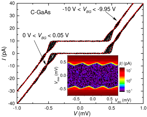
In our other devices, the InAs core is unexposed and always covered by another layer, either by the Al shell (device C-Al), by a protective GaAs shell (device E-GaAs) or by both (device C-GaAs). In the linear ohmic regime, at large bias voltage values, these devices exhibit a metallic behaviour: The transport is independent of the backgate value (no noticeable differences have been seen for in the range to 5 V). The I-V characteristics of the device C-GaAs at the backgate positions close to V and 0 V are shown in Fig. 3. Both sets of I-V characteristics are similar, confirming the metallic-like state of our device. The dashed lines correspond to a theoretical fit of the normal state used for a metallic SET with a SC island Grabert and Devoret (1992): The agreement between the measurements and the fit is very good. The parameters used for the fit are given in Table 1 and are the same for both measurements. The theoretical model fits also nicely the I-V characteristics of the other devices (not shown) in the normal state. This indicates that the QD measured is different from the one measured in the device E-Al as the properties of the devices (total resistance, charging energy and superconducting gap) do not change with the gate voltage. The inset is the stability diagram around V, exhibiting periodic and regular Coulomb diamonds. The metallic behaviour (i.e. absence of gate dependence in the transport besides the Coulomb blockade regime) is an evidence of the absence of undesirable QDs and that the transport is governed by only one intrinsic QD.
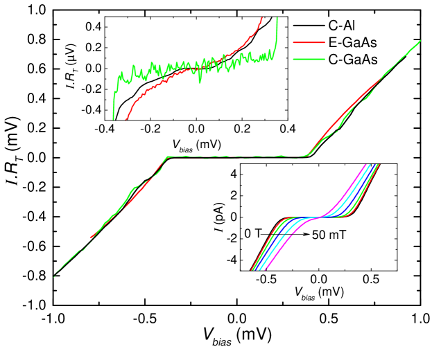
The comparison of the transport measurements at low bias voltage in the gate open state of the three devices is shown Fig. 4. To present all the samples on the same footing, we plot the product of the current and the resistance . The three devices are similar with the main difference being the charging energy. The upper inset shows the magnification of the measurements in the superconducting state. All devices have a superconducting gap similar to that of Al, eV. The slope of the I-V characteristics in the superconducting state is a signature of the hardness of the gap, and the ratio between the conductance in the superconducting state and in the normal state is , a measure of the hard gap of our system. As we have opaque transport channels, we now obtain an order of magnitude lower ratios proving that the gap in the NWs is even an order of magnitude harder than estimated earlier in Ref. Chang et al. (2015). The hard gap is not affected by etching the Al shell in the device E-GaAs, since the value measured equals to the gap at the proximity of the junctions, where the Al shell is not etched chemically. The lower inset shows the field dependence of a device similar to C-Al, from mT to 50 mT, close to the critical field measured at mT. The main effect of the magnetic field in the region is to close the superconducting gap: From this point of view, our devices are identical to metallic SETs and do not seem to present any additional interest. We will thus not focus on the normal state under field any longer.
The devices we show can be used for future studies of the properties of proximized superconductivity as our method is relatively non-invasive. Until now the SET regime in proximized InAs NWs was only achieved by tuning the potential of the wire with gates Albrecht et al. (2016); Higginbotham et al. (2015). However, the transport properties of the system can be very sensitive to the gate positions, and corrections have to be applied in case of cross-talk between the leads and the gates or between each gate. With one gate only, this is not the case, and we thus have a possibility to perform more advanced experiments, such as using the devices as a turnstile Pekola et al. (2008). The charging energy of our device can be easily increased by decreasing the dimensions of the NW (total length and diameter), the size of the QD (junctions spacing) or the size of the junctions.
The similarity between the devices C-Al and C-GaAs suggests that NWs with GaAs cover shell can be used for an SET setup, and the similarity between the devices C-GaAs and E-GaAs demonstrates that the GaAs layer prevents the formation of extra QDs and that the properties of the devices are not only caused by the Al layer, but also by the core. From the present results, it cannot yet be concluded if the GaAs cover shell improves the intrinsic properties of a NW (higher mobility of carriers or “harder” superconducting gap). When Al etching is necessary, to use electrostatic barriers for example, the GaAs cover shell may be used to prevent the appearance of unwanted QDs without affecting the proximity effect. This will give the opportunity to focus in the future on the intrinsic properties of the wires using devices with electrostatic barriers or with NWs half-covered with Al. Although it is possible to form ohmic contacts directly on InAs, this extra protective shell should also be compatible with good contacts to the external leads made afterwards.
IV In-gap measurements
We now present a study of a device similar to the device C-Al presented above, called C-Al’. The parameters of this device are listed in Table 1: the NW is smaller and the junctions are 1 m from each other. The Al layer of both extremities of the NW (beyond the junctions) has been chemically etched. Note that in this paragraph, conductance (and not resistance) measurements are shown. The device displays regular Coulomb diamonds with a stability diagram similar to the one given in the insert of Fig. 3. Therefore we will focus in the subgap regime with . Figure 5 shows the conductance measurements at zero field with the theoretical model (see below). In panel (a), the experimental (on the left hand side) and modelled (right hand side) stability diagram show clear Coulomb features in the subgap regime and the panels (b) and (c) are the measurements at constant and respectively. The difference between the gate open to the gate close state is more visible in panel (b) and a clear dip close to is present. Close to the ratio of the conductances reaches and at low bias outside the dip, highlighting the good quality of the proximized superconductivity. The panel (c) shows the Coulomb oscillations with the gate and their period doubling when V, i.e. when the bias voltage is smaller than the charging energy. These features - change of periodicity from 1 to 2 of the Coulomb oscillations and pronounced dip at low bias - are robust and have been observed in several devices. Similar pronounced minimum in the conductance as the one we observed has already been reported in proximized NWs Doh et al. (2008) and is attributed to the Coulomb blockade regime, but with a conductance ratio several orders of magnitude larger than in our device.
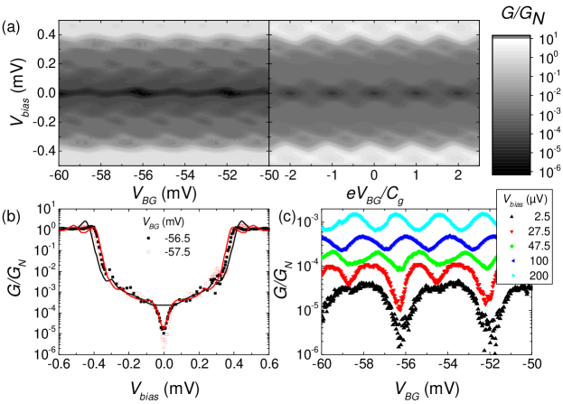
The model of the conductance measurements shown Fig. 5 is similar to the simple one used in Fig. 3 taking into account the normalized Dynes density of states (DOS) in the superconducting state Dynes et al. (1978, 1984)
| (1) |
with the Dynes parameter. The model shown in Fig. 5 uses and the parameters in Table 1. It reproduces relatively well the measurements as shown Fig. 5, except for the low bias voltage regime. Indeed, in this range the theoretical fit cannot reproduce the 2 periodicity of the oscillations and tends to overestimate the conductance. The origin of the 2-periodic signal and of the dip at low bias voltage is not clear yet, but they might come from localized in-gap states, which have been observed in similar devices using the same type of NWs Higginbotham et al. (2015). A more advanced model is therefore be needed to describe fully our system, and devices with higher charging energy would be useful in order to disentangle accurately the effect of these potential in-gap states to the Coulomb blockade regime.
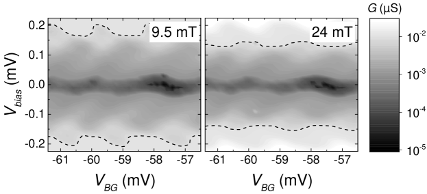
Figure 6 shows the stability diagram at low bias of the device C-Al’ at (left hand side) and (right side). The main effect of the magnetic field is to reduce the superconducting gap, as shown by the iso-conductance lines (dashed lines in Fig. 6 at nS) going closer to zero bias, the in-gap features at low bias voltage being relatively field insensitive below 30 mT. By increasing further the magnetic field, the 2-periodic signal will eventually vanish and the superconducting gap will close completely. The complete study of the magnetic field and temperature dependence of the subgap features are needed to get a better understanding.
V Conclusion
In conclusion we have demonstrated that InAs nanowires proximized with aluminium can be used as a single-electron transistor with a hard superconducting gap, by forming a fixed tunnel barrier based on the aluminium shell. Our results confirm that unwanted quantum dots can appear on the surface of the InAs core when bare. As for our devices the aluminium shell does not have to be etched, this prevents the formation of these extra quantum dots. They can be avoided when an additional thin protective layer of GaAs is inserted between the InAs and the aluminium, without seemingly degrading the transport or the superconducting properties of the system. Our technique provides a way to minimize the number of gates needed to nanowire-based devices. This gives an opportunity to use an InAs nanowire as an island of a single-electron transistor with the rich properties of a nanowire.
V.1 Acknowledgements
We thank M. Meschke and J. T. Peltonen for technical advice, and N. Paillet for help in plasma etching. This work has been supported by Academy of Finland (projects 272218 and 284594), by Danish National Research Foundation and by Microsoft Project Station Q. We acknowledge the availability of the facilities and technical support by Otaniemi research infrastructure for Micro and Nanotechnologies (OtaNano).
References
- Samuelson et al. (2004) L. Samuelson, C. Thelander, M. T. Björk, M. Borgström, K. Deppert, K. A. Dick, A. E. Hansen, T. Mårtensson, N. Panev, A. I. Persson, W. Seifert, N. Sköld, M. W. Larsson, and L. R. Wallenberg, “Semiconductor nanowires for 0d and 1d physics and applications,” Physica E: Low-dimensional Systems and Nanostructures 25, 313 – 318 (2004).
- Thelander et al. (2006) C. Thelander, P. Agarwal, S. Brongersma, J. Eymery, L. F. Feiner, A. Forchel, M. Scheffler, W. Riess, B. J. Ohlsson, U. Gösele, and L. Samuelson, “Nanowire-based one-dimensional electronics,” Materials Today 9, 28 – 35 (2006).
- Lieber and Wang (2007) C. M. Lieber and Z. L. Wang, “Functional nanowires,” MRS Bulletin 32, 99–108 (2007).
- Doh et al. (2005) Y.-J. Doh, J. A. van Dam, A. L. Roest, E. P. A. M. Bakkers, L. P. Kouwenhoven, and S. De Franceschi, “Tunable supercurrent through semiconductor nanowires,” Science 309, 272–275 (2005).
- Liang et al. (2015) D. Liang, J. Du, and X. P. A. Gao, “InAs nanowire devices with strong gate tunability: Fundamental electron transport properties and application prospects: A review,” Journal of Materials Science & Technology 31, 542 – 555 (2015).
- Li et al. (2006) Y. Li, F. Qian, J. Xiang, and C. M. Lieber, “Nanowire electronic and optoelectronic devices,” Materials Today 9, 18 – 27 (2006).
- Bryllert et al. (2006) T. Bryllert, L.-E. Wernersson, L.E. Froberg, and L. Samuelson, “Vertical high-mobility wrap-gated InAs nanowire transistor,” Electron Device Letters, IEEE 27, 323–325 (2006).
- Björk et al. (2004) M. T. Björk, C. Thelander, A. E. Hansen, L. E. Jensen, M. W. Larsson, L. R. Wallenberg, and L. Samuelson , “Few-electron quantum dots in nanowires,” Nano Letters 4, 1621–1625 (2004).
- van Dam et al. (2006) J. A. van Dam, Y. V. Nazarov, E. P. A. M. Bakkers, S. De Franceschi, and L. P. Kouwenhoven, “Supercurrent reversal in quantum dots,” Nature 442, 667–670 (2006).
- Sand-Jespersen et al. (2007) T. Sand-Jespersen, J. Paaske, B. M. Andersen, K. Grove-Rasmussen, H. I. Jørgensen, M. Aagesen, C. B. Sørensen, P. E. Lindelof, K. Flensberg, and J. Nygård, “Kondo-enhanced Andreev tunneling in InAs nanowire quantum dots,” Phys. Rev. Lett. 99, 126603 (2007).
- Lee et al. (2012) E. J. H. Lee, X. Jiang, R. Aguado, G. Katsaros, C. M. Lieber, and S. De Franceschi, “Zero-bias anomaly in a nanowire quantum dot coupled to superconductors,” Phys. Rev. Lett. 109, 186802 (2012).
- Chang et al. (2013) W. Chang, V. E. Manucharyan, T. S. Jespersen, J. Nygård, and C. M. Marcus, “Tunneling spectroscopy of quasiparticle bound states in a spinful Josephson junction,” Phys. Rev. Lett. 110, 217005 (2013).
- Lee et al. (2014) E. J. H. Lee, X. Jiang, M. Houzet, R. Aguado, C. M. Lieber, and S. De Franceschi, “Spin-resolved Andreev levels and parity crossings in hybrid superconductor-semiconductor nanostructures,” Nat. Nano. 9, 79–84 (2014).
- Nadj-Perge et al. (2010) S. Nadj-Perge, S. M. Frolov, E. P. A. M. Bakkers, and L. P. Kouwenhoven, “Spin-orbit qubit in a semiconductor nanowire,” Nature 468, 1084–1087 (2010).
- Krogstrup et al. (2015) P. Krogstrup, N. L. B. Ziino, W. Chang, S. M. Albrecht, M. H. Madsen, E. Johnson, J. Nygård, C. M. Marcus, and T. S. Jespersen, “Epitaxy of semiconductor-superconductor nanowires,” Nat. Mater. 14, 400–406 (2015).
- Chang et al. (2015) W. Chang, S. M. Albrecht, T. S. Jespersen, F. Kuemmeth, P. Krogstrup, J. Nygård, and C. M. Marcus, “Hard gap in epitaxial semiconductor-superconductor nanowires,” Nat. Nano. 10, 232–236 (2015).
- Lutchyn et al. (2010) R. M. Lutchyn, J. D. Sau, and S. Das Sarma, “Majorana fermions and a topological phase transition in semiconductor-superconductor heterostructures,” Phys. Rev. Lett. 105, 077001 (2010).
- Oreg et al. (2010) Y. Oreg, G. Refael, and F. von Oppen, “Helical liquids and Majorana bound states in quantum wires,” Phys. Rev. Lett. 105, 177002 (2010).
- Das et al. (2012) A. Das, Y. Ronen, Y. Most, Y. Oreg, M. Heiblum, and H. Shtrikman, “Zero-bias peaks and splitting in an Al-InAs nanowire topological superconductor as a signature of Majorana fermions,” Nat. Phys. 8, 887–895 (2012).
- Albrecht et al. (2016) S. M. Albrecht, A. P. Higginbotham, M. Madsen, F. Kuemmeth, T. S. Jespersen, J. Nygård, P. Krogstrup, and C. M. Marcus, “Exponential protection of zero modes in Majorana islands,” Nature 531, 206–209 (2016).
- Higginbotham et al. (2015) A. P. Higginbotham, S. M. Albrecht, G. Kirsanškas, W. Chang, F. Kuemmeth, P. Krogstrup, T. S. Jespersen, J. Nygård, K. Flensberg, and C. M. Marcus, “Parity lifetime of bound states in a proximitized semiconductor nanowire,” Nat. Phys. 11, – (2015).
- Fulton and Dolan (1987) T. A. Fulton and G. J. Dolan, “Observation of single-electron charging effects in small tunnel junctions,” Phys. Rev. Lett. 59, 109–112 (1987).
- Grabert and Devoret (1992) H. Grabert and M.H. Devoret, Single Charge Tunneling (Plenum, New-York, 1992).
- Averin and Pekola (2008) D. V. Averin and J. P. Pekola, “Nonadiabatic charge pumping in a hybrid single-electron transistor,” Phys. Rev. Lett. 101, 066801 (2008).
- Maisi et al. (2011) V. F. Maisi, O.-P. Saira, Yu. A. Pashkin, J. S. Tsai, D. V. Averin, and J. P. Pekola, “Real-time observation of discrete Andreev tunneling events,” Phys. Rev. Lett. 106, 217003 (2011).
- Zhong et al. (2005) Z. Zhong, Y. Fang, W. Lu, and C. M. Lieber, “Coherent single charge transport in molecular-scale Silicon nanowires,” Nano Letters 5, 1143–1146 (2005).
- Hofheinz et al. (2006) M. Hofheinz, X. Jehl, M. Sanquer, G. Molas, M. Vinet, and S. Deleonibus, “Simple and controlled single electron transistor based on doping modulation in Silicon nanowires,” Applied Physics Letters 89, 143504 (2006).
- Thelander et al. (2003) C. Thelander, T. Mårtensson, M. T. Björk, B. J. Ohlsson, M. W. Larsson, L. R. Wallenberg, and L. Samuelson, “Single-electron transistors in heterostructure nanowires,” Applied Physics Letters 83, 2052–2054 (2003).
- Popovitz-Biro et al. (2011) R. Popovitz-Biro, A. Kretinin, P. Von Huth, and H. Shtrikman, “InAs/GaAs core-shell nanowires,” Crystal Growth & Design 11, 3858–3865 (2011).
- van Tilburg et al. (2010) J. W. W. van Tilburg, R. E. Algra, W. G. G. Immink, M. Verheijen, E. P. A. M. Bakkers, and L. P. Kouwenhoven, “Surface passivated InAs/InP core/shell nanowires,” Semiconductor Science and Technology 25, 024011 (2010).
- Chia et al. (2012) A. C. E. Chia, M. Tirado, Y. Li, S. Zhao, Z. Mi, D. Comedi, and R. R. LaPierre, “Electrical transport and optical model of GaAs-AlInP core-shell nanowires,” Journal of Applied Physics 111, 094319 (2012).
- Lin et al. (2013) A. Lin, J. N. Shapiro, A. C. Scofield, B. L. Liang, and D. L. Huffaker, “Enhanced InAs nanopillar electrical transport by in-situ passivation,” Applied Physics Letters 102, 053115 (2013).
- Holloway et al. (2013) G. W. Holloway, Y. Song, C. M. Haapamaki, R. R. LaPierre, and J. Baugh, “Electron transport in InAs-InAlAs core-shell nanowires,” Applied Physics Letters 102, 043115 (2013).
- Ganjipour et al. (2014) B. Ganjipour, S. Sepehri, A. W. Dey, O. Tizno, B. M. Borg, K. A. Dick, L. Samuelson, L.-E. Wernersson, and C. Thelander, “Electrical properties of GaSb/InAsSb core/shell nanowires,” Nanotechnology 25, 425201 (2014).
- Gloos et al. (2003) K. Gloos, P. J. Koppinen, and J. P. Pekola, “Properties of native ultrathin Aluminium oxide tunnel barriers,” Journal of Physics: Condensed Matter 15, 1733 (2003).
- Wunnicke (2006) O. Wunnicke, “Gate capacitance of back-gated nanowire field-effect transistors,” Applied Physics Letters 89, 083102 (2006).
- Bleszynski et al. (2007) A. C. Bleszynski, F. A. Zwanenburg, R. M. Westervelt, A. L. Roest, E. P. A. M. Bakkers, and L. P. Kouwenhoven, “Scanned probe imaging of quantum dots inside InAs nanowires,” Nano Letters 7, 2559–2562 (2007).
- Boyd et al. (2011) E. E. Boyd, K. Storm, L. Samuelson, and R. M. Westervelt, “Scanning gate imaging of quantum dots in 1d ultra-thin InAs/InP nanowires,” Nanotechnology 22, 185201 (2011).
- Schroer and Petta (2010) M. D. Schroer and J. R. Petta, “Correlating the nanostructure and electronic properties of InAs nanowires,” Nano Letters 10, 1618–1622 (2010).
- Weis et al. (2014) K. Weis, S. Wirths, A. Winden, K. Sladek, H. Hardtdegen, H. Lüth, D. Grützmacher, and T. Schäpers, “Quantum dots in InAs nanowires induced by surface potential fluctuations,” Nanotechnology 25, 135203 (2014).
- Pekola et al. (2008) J. P. Pekola, J. J. Vartiainen, M. Möttönen, O.-P. Saira, M. Meschke, and D. V. Averin, “Hybrid single-electron transistor as a source of quantized electric current,” Nat. Phys. 4, 120–124 (2008).
- Doh et al. (2008) Y.-J. Doh, S. De Franceschi, E. P. A. M. Bakkers, and L. P. Kouwenhoven, “Andreev reflection versus Coulomb blockade in hybrid semiconductor nanowire devices,” Nano Letters 8, 4098–4102 (2008), NoStop
- Dynes et al. (1978) R. C. Dynes, V. Narayanamurti, and J. P. Garno, “Direct measurement of quasiparticle-lifetime broadening in a strong-coupled superconductor,” Phys. Rev. Lett. 41, 1509–1512 (1978).
- Dynes et al. (1984) R. C. Dynes, J. P. Garno, G. B. Hertel, and T. P. Orlando, “Tunneling study of superconductivity near the metal-insulator transition,” Phys. Rev. Lett. 53, 2437–2440 (1984).