Superlattice gain in positive differential conductivity region
Abstract
We analyze theoretically a superlattice structure proposed by A. Andronov et al. [JETP Lett 102, 207 (2015)] to give Terahertz gain for an operation point with positive differential conductivity. Here we confirm the existence of gain and show that an optimized structure displays gain above 20 cm-1 at low temperatures, so that lasing may be observable. Comparing a variety of simulations, this gain is found to be strongly affected by elastic scattering. It is shown that the dephasing modifies the nature of the relevant states, so that the common analysis based on Wannier-Stark states is not reliable for a quantitative description of the gain in structures with extremely diagonal transitions.
pacs:
72.10.-d, 72.20.-iSemiconductor superlattices Esaki and Tsu (1970) (SLs) had always been considered as an interesting candidate for THz gain materials due to the Bloch gain Ktitorov et al. (1972), which was finally experimentally confirmed more than 30 years laterShimada et al. (2003); Savvidis et al. (2004); Sekine and Hirakawa (2005). However, this type of gain is intrinsically connected with the negative differential conductivity in the current-field relation, so that the formation of field domainsEsaki and Chang (1974); Grahn (1995); Wacker (2002); Bonilla and Grahn (2005) strongly limits its observation and practical use. As an alternative, it was suggested Andronov et al. (2009) that gain can be present in the positive differential conductivity region of SLs where resonant tunneling over several barriers Schneider et al. (1990); Sibille et al. (1998); Helm et al. (1999) is relevant. The idea is to operate the SL slightly below the tunneling resonance from the ground state of well to the excited state in the next-neighboring well (see the inset of FIG. 1), which guarantees positive differential conductivity. At the same time, gain is suggested for the strongly diagonal transition to the excited state in the well , which is actually lower in energy than the ground state in well . More detailed experimental studies confirmed the suggested shape of the current-field relation, but were not conclusive with respect to THz gainAndronov et al. (2015). Thus the question remains, whether this type of gain exists at all and whether it is strong enough to overcome losses. In order to address this question, we performed detailed simulations with our non-equilibrium Green’s function (NEGF) simulation scheme Wacker et al. (2013), which are reported here. We find that this particular gain mechanism exists, but that it is not particularly strong for the structure proposed. Testing different doping densities and layer sequences, we observe gain above 20/cm at low temperatures, which could overcome losses in typical THz waveguides Faist (2013). We noticed that dephasing strongly reduces this type of gain with an extremely diagonal transition. This can be quantified by the eigenstates of the lesser Green’s function, which represent better states to estimate gain than the conventional eigenstates of the Hamiltonian called Wannier-Stark (WS) states.
The NEGF model allows for a self-consistent evaluation of the transport with respect to both elastic and inelastic scattering as well as interactions with an electromagnetic field in semiconductor heterostructure devices Lee et al. (2006); Schmielau and Pereira (2009); Kubis et al. (2009); Haldaś and et al. (2011); Grange (2015). In particular, it is suitable for the study of semiconductor SLs, as it contains simpler approaches, such as miniband transport Esaki and Tsu (1970), Wannier-Stark hopping Tsu and Döhler (1975); Calecki et al. (1984), or sequential tunneling Kazarinov and Suris (1971) as limiting cases Wacker and Jauho (1998).
In NEGF models, scattering is treated by self-energies that are evaluated self-consistently until convergence is reached. These objects are functions of both momentum and energy, but in our implementation they are effectively treated as only energy dependent, and evaluated at a representative set of momentum transfers for the scattering matrix elementsWacker et al. (2013). This set is chosen by a typical energy transfer , fitted to give scattering matrix elements matching those calculated with thermalized subbands for other low doped heterostructures. Here, we apply also different values, in order to mimic increased or decreased scattering environments. In this study all samples considered were assumed to be homogeneously doped. Unless stated otherwise, we also keep the lattice temperature fixed at K, where we consider the model to be both robust and accurate.
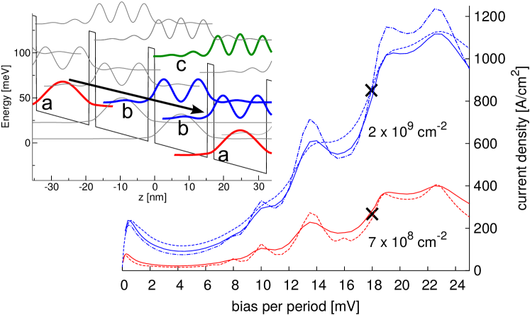
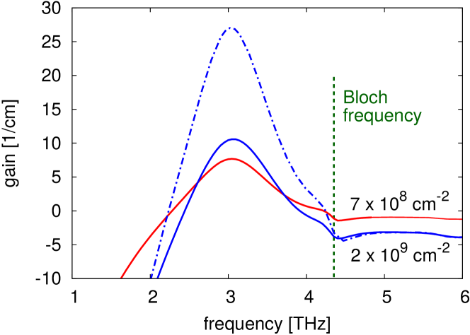
FIG. 1 shows the calculated current-voltage characteristics for the device of Ref. Andronov et al., 2015 (red solid line for a doping of per period). The peak structure agrees reasonably well with the experimental data shown in FIG. 4 of Ref. Andronov et al., 2015. For comparison, the experimental shoulder at 19 mV per period, where the ground state is in resonance with the excited state of the 2nd nearest neighbor well, shows a current density of . In the following we focus on the operation point at 18 mV per period, which is a stable operation point with positive differential conductivity. The inset in FIG. 1 shows the Wannier levels at this field. FIG. 2 shows the calculated gain (at weak cavity field). For the nominal structure (red solid line) it remains well below 10/cm, which is probably too small to overcome the total losses.
In the following we will employ a strict naming convention for the SL states where will give the period index, with 0 for the central period, and for the state index. Here, Wannier states, are denotes by letters and Wannier-Stark states (WS states, which are the eigenstates of the Hamiltonian) by roman numbers . The tunneling resonance at the current peak at 19 mV per period is thus between Wannier levels and . At 18 mV per period the resonance between these levels is slightly detuned, so that the WS state is dominated by but has significant admixtures from and . Similarly, the WS state is dominated by with significant admixtures from , , and . These states are displayed in FIG. 3 (c) by full lines. The state is lower in energy than and has thus a significantly larger occupation.
Now the state , which is equivalent to , but shifted to the right and down in energy, is about 14.7 meV below the state . As both states extend over several periods they overlap significantly and furthermore there is inversion for the corresponding transition. We can attribute the gain shown in FIG. 2 to this transition, where a slight red shift can be explained by dispersive gain Terazzi et al. (2007).
As an attempt to improve inversion and gain, the doping was increased to give a sheet density three times higher than the nominal sample. The result on current and gain is shown in FIG. 1 and FIG. 2, respectively. As expected the current density increases approximately by a factor three. However, the peak gain increases only slightly at 77 K. Significantly higher values are found at lower temperatures, where our model suggests gain above 20/cm at 40 K.111However, we refrain from making a definite statement on specific values, as our model showed inaccuracies for some quantum cascade lasers at such low temperatures. Furthermore, in both samples there are small signatures of Bloch gain at around 4.2 THz and we also observe that the high doped sample has more dark absorption at frequencies far from the gain transition.
In the following, we want to study, why the increase of gain with doping is limited, so that its practical use appears questionable. A naive guess, would be an increase of gain by a factor three just like the current. However, the inversion might not be proportional to the doping and the linewidth changes with doping. In order to study these effects, we use the standard estimate for the gain using Fermi’s Golden Rule (FGR)
| (1) |
where is the energy difference between the initial and final states, is the inversion, the dipole matrix element, is the refractive index and is the full width half maximum of the gain peak. These variables can be extracted from the full NEGF model where we diagonalize the Hamiltonian including the real parts of the self-energies, on the diagonal in order to shift the single particle energy levels, to get the WS states. Here we approximate the linewidth as the sum of the lifetimes of the two states involved, .
| [1/cm2] | |||||
| (meV) | 14 | 6.2 | 6.2 | 3.2 | 4.7 (40 K) |
| (meV) | 1.3 | 2.6 | 3.4 | 5.0 | 2.3 (40 K) |
| NEGF | 19.2 | 7.30 | 9.50 | -1.64 | 25.9 |
| FGR(WS) | 20.7 | 11.8 | 26.6 | 19.8 | 37.5 |
| FGR() | 23.8 | 8.90 | 15.4 | 6.39 | 29.2 |
The result of this estimate is shown in TAB. 1 for a set of different model systems. The second and third column of TAB. 1 refer to our standard simulation parameters with meV at 77 K, as used in FIGS. 1-2 (full lines). Furthermore, we also performed simulations with altered . The data in the first/fourth column are for decreased/increased scattering compared to their neighboring column. This is reflected by the respective width of the ground state , which is extracted from the NEGF calculation. The current simulations for these parameters are shown by dashed lines in FIG. 1. The minor changes in current can be understood by a slight broadening/sharpening of the tunneling resonances for increased/decreased scattering, respectively. The fifth column in TAB. 1 gives results for 40 K using our standard temperature dependent .
Let us first consider the estimate from FGR (1) with the common WS states in TAB. 1. Here we find, that the peak gain follows essentially the doping density divided by , which shows that the inversion is essentially proportional to doping, and all other ingredients, except for the broadening, are constant. In contrast, the NEGF calculation shows a much stronger decrease of gain with . While a part of the differences may be attributed to the widening of other absorbing transitions, the large extent is stunning.
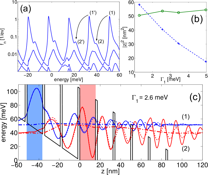
To understand this discrepancy we analyze the eigenstates of the lesser Green’s function (which can be viewed as the energetically resolved density matrix) and the corresponding wavefunctions following Ref. Lee et al., 2006. The eigenvalues for the nominal case with are plotted in FIG. 3 (a) for . The eigenvalues show two sets of peaks, and , corresponding to the ground and excited level. They also visualize the inversion at an energy of 12 meV (indicated by arrows), corresponding to 3 THz. As the eigenvalues are sorted by size in the diagonalization process, we see anti-crossings where the different eigenstates passes each other, so that the state at the eigenvalue indicated by (2) is not the same as the one at (1) since they are separated by at least one anti-crossing.
At the eigenvalue peaks (1) and (2) we plot the corresponding eigenstates in FIG. 3 (c) together with the WS states. From this plot it is possible to see that compared to the WS states, the wavefunction corresponding to the eigenstate is slightly more localized than the WS state . For these simulation parameters this leads to a decrease of the dipole matrix element. In FIG. 3 (b) the modulus square of the dipole matrix elements are plotted versus the width of the ground state. The WS states show small variations due to meanfield and renormalization due to scattering, but are otherwise constant. In contrast, the dipole matrix elements calculated by the eigenstates of the Green’s function, are comparable at low scattering but provide a strong decrease with increasing scattering. These dipole matrix elements can be applied in FGR (1), and the results are given in the lowest line of TAB. 1. They actually follow the trend of the full calculation, which demonstrates the relevance of these eigenstates. The result by FGR naturally overestimates the gain slightly, as we consider the gain from only one transition while all other (mostly absorbing) transitions are fully taken into account in the NEGF model.
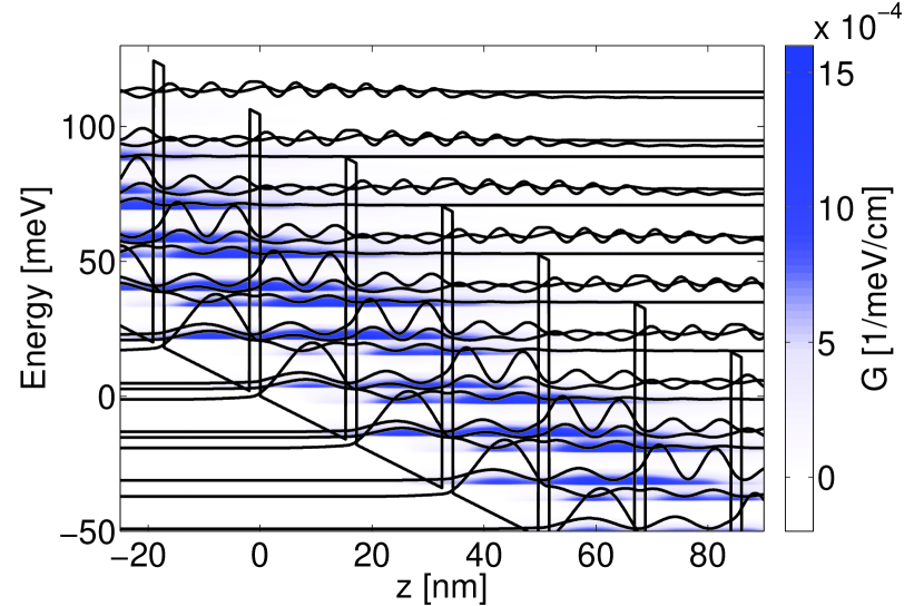
The strong -dependence of the eigenstates of the lesser Green’s function is reflected by dephasing, which affects the coherence length. In this particular situation, the gain is highly diagonal and is thus dependent on these spatial coherences. This is further demonstrated in FIG. 4, where the gain stripes extend over more than 50 nm.
As a complement to changing doping, we also tried to optimized the SL by modifying the well and barrier widths. Here we present results for the structures wide/narrow, where the well is increased/decreased by 4 monolayers, respectively, and the structure thin, where the barrier is decreased by 2 monolayers compared to the nominal sample. The sheet doping density was kept constant at .
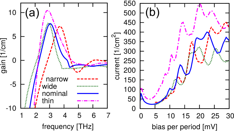
In FIG. 5 we display gain and current for the samples, which shows that adjusting the well width merely causes a shift in the peak frequency, while thinner barriers improve the performance of the gain medium slightly.
In conclusion, we have shown that the NEGF model predicts gain in the structure from Ref. Andronov et al., 2015. However, the value is below 10/cm at 77 K, which hardly allows for lasing due to waveguide losses. Increasing the doping, lasing at 40 K appears feasible. Further slight optimization by reducing the thickness of the barriers may be possible.
For this highly diagonal transition, the gain is strongly dependent on the scattering. This can be demonstrated by the eigenstates of the lesser Green’s function, which essentially differ from the WS states in this case. We demonstrated that these unconventional states are more appropriate to calculate the dipole matrix elements for a quantitative description of gain by Fermi’s golden rule.
Acknowledgments: We thank A. Andronov and J. Faist for helpful discussions and the Swedish Research Council for financial support.
References
- Esaki and Tsu (1970) L. Esaki and R. Tsu, IBM J. Res. Dev. 14, 61 (1970).
- Ktitorov et al. (1972) S. A. Ktitorov, G. S. Simin, and V. Y. Sindalovskii, Sov. Phys.–Sol. State 13, 1872 (1972), [Fizika Tverdogo Tela 13, 2230 (1971)].
- Shimada et al. (2003) Y. Shimada, K. Hirakawa, M. Odnoblioudov, and K. A. Chao, Phys. Rev. Lett. 90, 046806 (2003).
- Savvidis et al. (2004) P. G. Savvidis, B. Kolasa, G. Lee, and S. J. Allen, Phys. Rev. Lett. 92, 196802 (2004).
- Sekine and Hirakawa (2005) N. Sekine and K. Hirakawa, Phys. Rev. Lett. 94, 057408 (2005).
- Esaki and Chang (1974) L. Esaki and L. L. Chang, Phys. Rev. Lett. 33, 495 (1974).
- Grahn (1995) H. T. Grahn, ed., Semiconductor Superlattices, Growth and Electronic Properties (World Scientific, Singapore, 1995).
- Wacker (2002) A. Wacker, Phys. Rep. 357, 1 (2002).
- Bonilla and Grahn (2005) L. L. Bonilla and H. T. Grahn, Reports on Progress in Physics 68, 577 (2005).
- Andronov et al. (2009) A. A. Andronov, E. P. Dodin, D. I. Zinchenko, and Y. N. Nozdrin, Journal of Physics: Conference Series 193, 012079 (2009).
- Schneider et al. (1990) H. Schneider, H. T. Grahn, K. v. Klitzing, and K. Ploog, Phys. Rev. Lett. 65, 2720 (1990).
- Sibille et al. (1998) A. Sibille, J. F. Palmier, and F. Laruelle, Phys. Rev. Lett. 80, 4506 (1998).
- Helm et al. (1999) M. Helm, W. Hilber, G. Strasser, R. De Meester, F. M. Peeters, and A. Wacker, Phys. Rev. Lett. 82, 3120 (1999).
- Andronov et al. (2015) A. Andronov, E. Dodin, D. Zinchenko, Y. Nozdrin, M. Ladugin, A. Marmalyuk, A. Padalitsa, V. Belyakov, I. Ladenkov, and A. Fefelov, JETP Lett+ 102, 207 (2015).
- Wacker et al. (2013) A. Wacker, M. Lindskog, and D. Winge, Sel. Top. in Quantum Electron., IEEE Journal of 19, 1200611 (2013).
- Faist (2013) J. Faist, Quantum Cascade Lasers (Oxford University Press, Oxford, 2013).
- Lee et al. (2006) S.-C. Lee, F. Banit, M. Woerner, and A. Wacker, Phys. Rev. B 73, 245320 (2006).
- Schmielau and Pereira (2009) T. Schmielau and M. Pereira, Appl. Phys. Lett. 95, 231111 (2009).
- Kubis et al. (2009) T. Kubis, C. Yeh, P. Vogl, A. Benz, G. Fasching, and C. Deutsch, Phys. Rev. B 79, 195323 (2009).
- Haldaś and et al. (2011) G. Haldaś and, A. Kolek, and I. Tralle, Quantum Electronics, IEEE Journal of 47, 878 (2011).
- Grange (2015) T. Grange, Phys. Rev. B 92, 241306 (2015).
- Tsu and Döhler (1975) R. Tsu and G. Döhler, Phys. Rev. B 12, 680 (1975).
- Calecki et al. (1984) D. Calecki, J. F. Palmier, and A. Chomette, J. Phys. C: Solid State Phys. 17, 5017 (1984).
- Kazarinov and Suris (1971) R. F. Kazarinov and R. A. Suris, Sov. Phys. Semicond. 5, 707 (1971).
- Wacker and Jauho (1998) A. Wacker and A.-P. Jauho, Phys. Rev. Lett. 80, 369 (1998).
- Terazzi et al. (2007) R. Terazzi, T. Gresch, M. Giovannini, N. Hoyler, N. Sekine, and J. Faist, Nature Physics 3, 329 (2007).
- Note (1) However, we refrain from making a definite statement on specific values, as our model showed inaccuracies for some quantum cascade lasers at such low temperatures.