Inverse design of resonant nanostructures for extraordinary optical transmission of periodic metallic slits
Abstract
This paper presents the inverse design of resonant nanostructures for the extraordinary optical transmission of periodic metallic slits, where the topology optimization approach is utilized to implement the inverse design procedure and find the geometrical configurations of the nanostructures. By the inverse design method, the subwavelength-size resonant nanostructures, localized at the inlet and outlet sides of the periodic metallic slits, are derived with transmission peaks at the prescribed incident wavelengths. And the transmissivity is enhanced by effective excitation and guidance of surface plasmon polariton at the inlet side of the slits, coherently resonance of surface plasmon polariton inside the slits and radiation of the photonic energy at the outlet side of the slits. The transmission peaks of the periodic metallic slits, with inversely designed resonant nanostructures, are raised along with the red shift of the incident wavelength. The presentation of the transmission peak of periodic metallic slits can be controlled and localized at a desired frequency, by specifying the incident wave with the wavelength corresponding to the desired frequency for the inverse design procedure. By maximizing the minimum transmissivity of the periodic metallic slits with incident wavelengths in a prescribed wavelength range, the extraordinary optical transmission bandwidth can be enlarged, and the sensitivity of transmissivity to wavelength can be decreased equivalently.
Keywords: Inverse design; resonant nanostructures; extraordinary optical transmission; periodic metallic slits; topology optimization
1 Introduction
Extraordinary optical transmission (EOT) is the phenomenon of greatly enhanced transmission of light through a subwavelength aperture in an otherwise opaque metallic film which has been patterned with a regularly repeating periodic structure. It was first described by Ebbesen et al in 1998 [1]. In EOT, the regularly repeating structures enable much higher transmissivity to occur, up to several orders of magnitude greater than that predicted by classical aperture theory. And the mechanism of EOT is attributed to the scattering of surface plasmon polaritons (SPPs) [2, 3]. EOT offers one key advantage over a surface plasmonic resonance (SPR) device, an inherently nanometer-micrometer scale device, and it is particularly amenable to miniaturization. Tremendous potential applications of EOT include several newly emerging areas, e.g. subwavelength optics, opto-electronic devices, wavelength-tunable filters, optical modulators [4, 5, 6, 3], left-handed metamaterial and chemical sensing [7]. To achieve the required transmission performance, metallic layouts with subwavelength apertures, e.g. subwavelength hole array [1], periodic slit array, tapered slits [8], diatomic chain of slit-hole [9], groove array flanking slit [10] and bull’s eye structures[11], have been proposed for EOT; and parametric optimization of metallic layouts with subwavelength apertures have been implemented to enhance the transmissivity [12, 13]. Most of these researches are focused on enhancing EOT with nanostructures derived based on physical intuition. The more challenging problem problem can be inverse design or determination of the geometrical configurations of the nanostructures for enhancing EOT. Therefore, this paper is devoted to inversely designing resonant nanostructures to enhance the extraordinary optical transmission of periodic metallic slits, where the topology optimization approach is utilized to implement the inverse design method and find the geometrical configurations of the nanostructures.
Recently, it is shown that topology optimization can be used to inversely determine geometrical configuration of structures and achieve the inverse design of devices in elastics, hydrodynamics, electromagnetics or photonics et al [14, 15, 16, 17]. In electromagnetics or photonics, topology optimization approach has been applied in the inverse design of beamsplitters [18, 19], photonic crystals [21, 20, 22], cloaks [23, 24, 25], metamaterials [28, 27, 26], excitation of SPPs and LSPRs [29, 30], and electromagnetic and optical antennas [31, 33, 32, 34]. In topology optimization, the structure is inversely determined using the material penalization approach, where the design variable is used to represent the material distribution and geometrical configuration. The design variable is evolved to a indicator function using the robust gradient based optimization algorithm, e.g. the method of moving asymptotes (MMA) [35]. Therefore, the topology optimization approach is chosen to implement the inverse design of the nanostructures of the periodic metallic slits for EOT.
2 Methodology
Cross-section of periodic metallic slits with infinite thickness is illuminated in Fig. 1 with a uniform monochromatic transverse magnetic (TM) wave propagation. The computational domain is set to be one period of the metallic slits. The topology optimization approach is utilized to inversely design the nanostructures localized in the bilateral regions of the preset metallic slits. Then the design domain, where the design variable is defined, is set to be these two bilateral regions. To truncate the infinitive free space, the first order absorbing boundary condition is imposed on the inlet () and outlet () boundaries of the computational domain, and the periodic boundary condition is imposed on the left () and right () boundaries of the slit to reduce the computational cost. Based on the above computational setup, the inverse design problem is to find the geometrical configurations of the bilateral nanostructures for the preset slit to maximize the transmission of the electromagnetic energy. The propagating wave in the metallic slits is time-harmonic TM wave governed by the Maxwell’s equations in two dimensions, which can be reformulated into the scalar Helmholtz equation expressed as
| (1) |
where the scattered-field formulation, with , is used to reduce the dispersion error; and are the scattered and incident fields, respectively; and are the relative permittivity and permeability, respectively; is the free space wave number with , and respectively representing the angular frequency, free space permittivity and permeability; is the computational domain; is the wave vector; the time dependence of the fields is given by the factor , with representing the time; is the unit outward normal vector at ; is the imaginary unit; and are respectively the inlet and outlet boundaries of the photonic energy; and and are respectively the source and destination boundary of the periodic boundary pair, with lattice vector . The incident field is set to be the parallel-plane wave with unit amplitude.
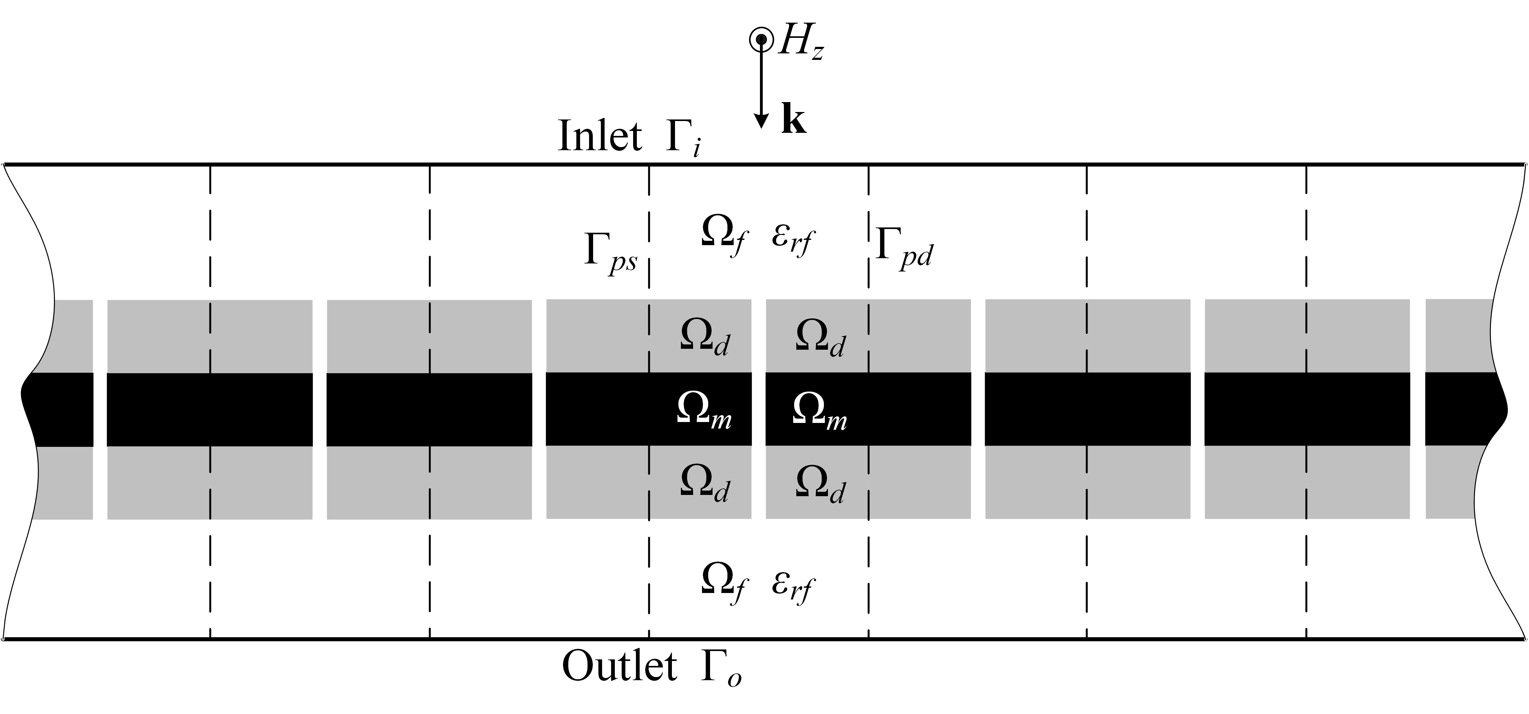
The topology optimization approach, chosen to carry out inverse design of bilateral nanostructures for enhancing EOT of periodic metallic slits, is implemented based on the material interpolation between the metal and free space in the design domain. In EOT, the used noble metal is usually nonmagnetic, e.g. silver (Ag) and gold (Au). Therefore, the permeability is set to be 1. Then, only the spatial distribution of relative permittivity needs to be determined in the inverse design procedure. In the visible light region, the relative permittivity of noble metal can be described by the Drude model
| (2) |
where is the high-frequency bulk permittivity; is the angular frequency of the incident wave; is the bulk plasmon frequency; is the collision frequency. The material interpolation is performed using the material density representing the geometrical configuration [39], and the material density is introduced with the values and respectively representing free space and metal. Because the surface plasmons are presented at the surface of noble metal, the electromagnetic field decays exponentially; hence, the material density should decays rapidly away from 1 to mimic the metal surface. Thus, the material interpolation is set to be the hybrid of logarithmic and power law approaches
| (3) |
where is the relative permittivity in the design domain; is the material density. The material density is derived by filtering and projecting the design variable valued in . During the evolution of the design variable, filtering is implemented by the density filter to enforce a minimum length scale of the derived geometrical configuration [36]
| (4) |
where is the filter radius chosen based on numerical experiments [37]; is the filtered design variable. And projecting is implemented by the threshold projection to remove the gray area in the derived geometrical configuration [38]
| (5) |
where and are the threshold and projection parameters for the threshold projection, respectively. On the choice of the values of and , one can refer to [40, 41].
EOT is featured by its high transmission of the photonic energy through periodic subwavelength metallic apertures. The input and output transmission power for one period of the metallic slits can be measured by the integration of the average Poynting vector on the the inlet and outlet sides of the computational domain
| (6) |
| (7) |
where and are the input and output transmission power, respectively; is the electric fields corresponding to the incident magnetic wave ; is the total electric fields; is the total magnetic fields; operator is used to extract the real part of an expression; represents the conjugate of the complex variable. The objective of the inverse design procedure can be chosen to maximize the transmissivity defined as the normalized transmission power
| (8) |
Then the inverse design problem for the bilateral nanostructures of periodic metallic slits is to maximize the transmissivity defined in Equ. 8, which is constrained by Equ. 1 and Equ. 4 with design variable valued in . The gradient-based iterative procedure, method of moving asymptotes [35], is applied to update the design variable and maximize the transmissivity. And the gradient information is obtained using the continuous adjoint method [42]
| (9) |
where is the adjoint of the filtered design variable . is derived by solving the adjoint equations of the wave equation in Equ. 1 and density filter in Equ. 4
| (10) |
| (11) |
where and represent the adjoint of and the integral function of Equ. 7, respectively; and are the first order Hilbert functional spaces defined on and .
3 Results and discussion
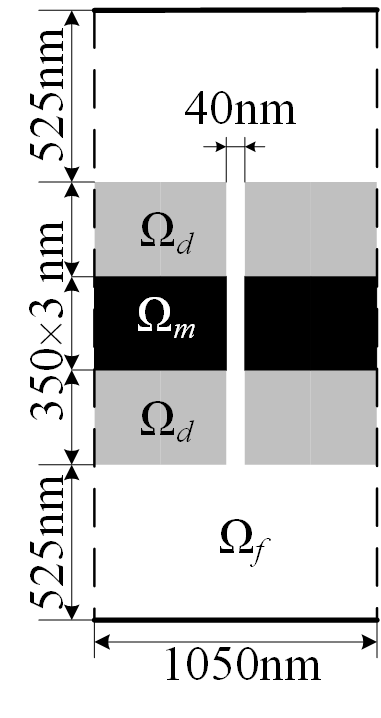
Using the outlined topology optimization based inverse design procedure for enhancing EOT of periodic metallic slits, the bilateral nanostructures are investigated as follows. The noble metal is chosen to be Ag, with high-frequency bulk permittivity , bulk plasmon frequency rad/s, and collision frequency rad/s derived by fitting the experimental data in the literatures [43]. The sizes of the computational domain shown in Fig. 1 are set to be the typical values: nm for the periodic length of the metallic slits, nm for the slit width, nm for the thickness of the fixed Ag layer , and nm for the thickness of the design domain (Fig. 2). The incident wavelength is scanned in the visible light region ( nm). For different incident wavelengths, the nanostructures sticking to the metallic slits are derived as shown in Fig. 3af, with corresponding magnetic field distribution shown in Fig. 4af. These results demonstrate that the inversely derived nanostructures sticking to the inlet side of the subwavelength slits excite SPPs and guide the SPPs propagating into the metallic slits; the two streams of SPPs in the slits propagate along the two sides of the metallic slits, couple with each other, the Fabry-Pérot resonance of these two streams of SPPs is established sequentially with strengthened transmission [44, 45, 46, 47, 48]; at the outlet side, the resonating SPPs is scattered and radiated into free space by the inversely derived nanostructures; at last, EOT is achieved and enhanced by the inversely designed bilateral nanostructures, with resonance peaks demonstrated in the transmission spectra shown in Fig. 5.


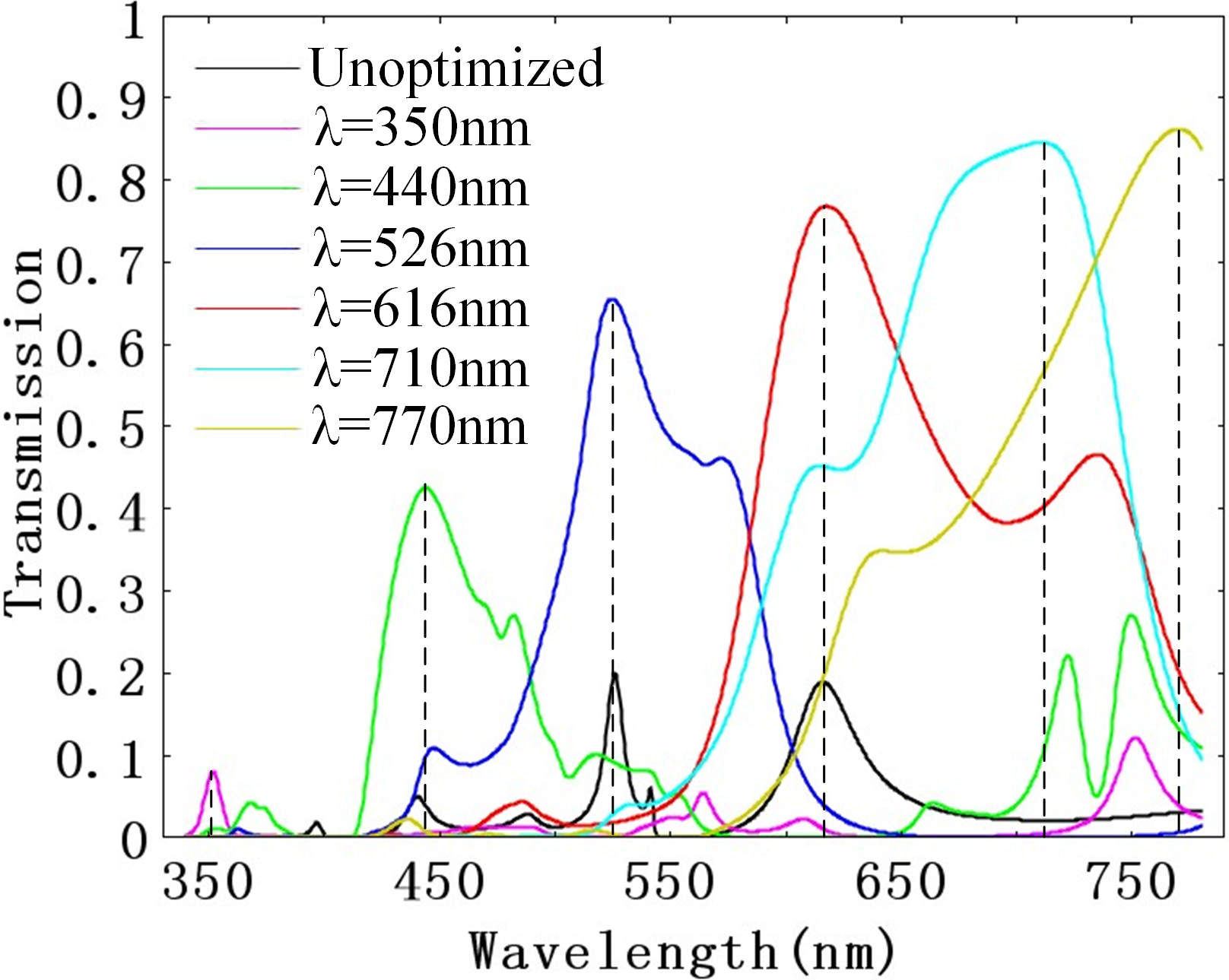
The effectivity of the inversely designed bilateral nanostructures on enhancing the EOT performance of periodic metallic slits can be demonstrated furthermore by the transmission spectra in Fig. 5. There are two transmission peaks at the wavelength nm and nm for the periodic metallic slits without bilateral nanostructures. These transmission peaks are enhanced and times respectively by the inversely designed bilateral nanostructures with geometrical configurations shown in Fig. 3c and 3d. In Fig. 5, the transmission peaks are presented at the specified incident wavelengths in the inverse design procedure, and the peak is red shifted along with the increase of the incident wavelength. Therefore, the derived nanostructures result in the resonant EOT performance at the specified incident wavelength, i.e. the nanostructures derived by the inverse design method are resonant for EOT of periodic metallic slits. Sequentially, this inverse design method can be used to control the presentation of the transmission peak at a desired frequency, by specifying the incident wavelength corresponding to the desired frequency in the inverse design procedure.
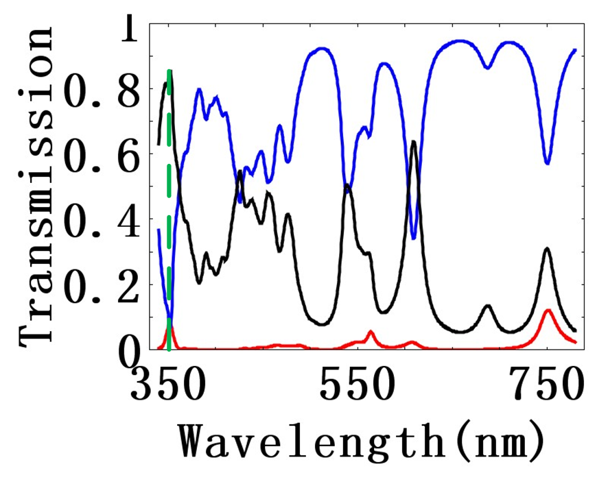
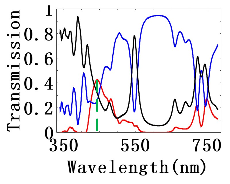
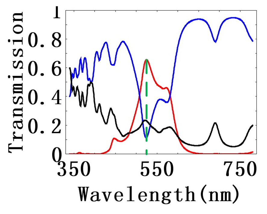
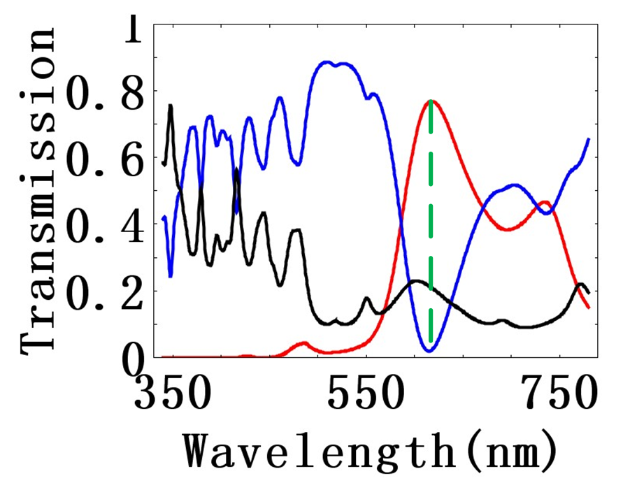
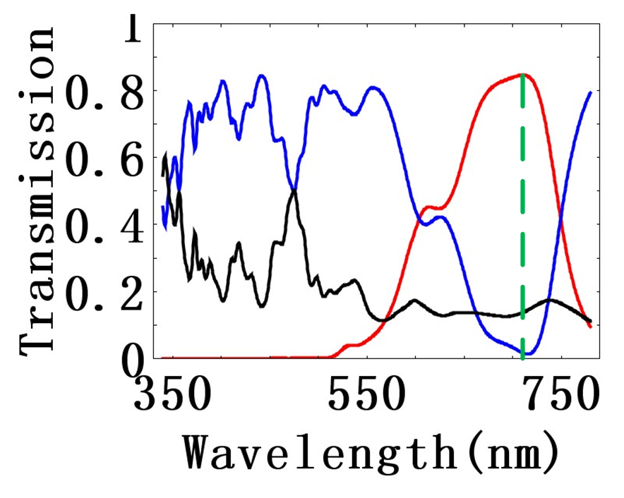
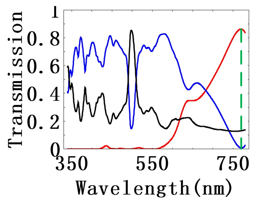
The transmission spectra in Fig. 5 also demonstrates that the transmission peak is raised along with the red shift of the incident wavelength. This is mainly caused by the large absorption of the photonic energy and short propagation distance of SPP in the short-wavelength region, and relatively low absorption and long propagation distance of SPP in the long-wavelength region. And this can be confirmed by the comparison of transmission, reflection and absorption spectra of the periodic metallic slits with inversely designed bilateral nanostructures (Fig. 6). The absorption spectra in Fig. 6 also demonstrate that the periodic metallic slits with inversely derived bilateral nanostructures have resonant light absorption performance, e.g. of the photonic energy is absorbed by the slits shown in Fig. 3b at the incident wavelength 390nm.

The discussed inverse design method can be extended to enlarge the EOT bandwidth of the periodic metallic silts. And by enlarge the EOT bandwidth, the sensitivity of the transmissivity to the incident wavelengths can be reduced in a specified wavelength range. Then one inverse design objective is formulated for the bilateral nanostructures of the periodic metallic slits at a central incident wavelength with specified wavelength perturbation range
| (12) |
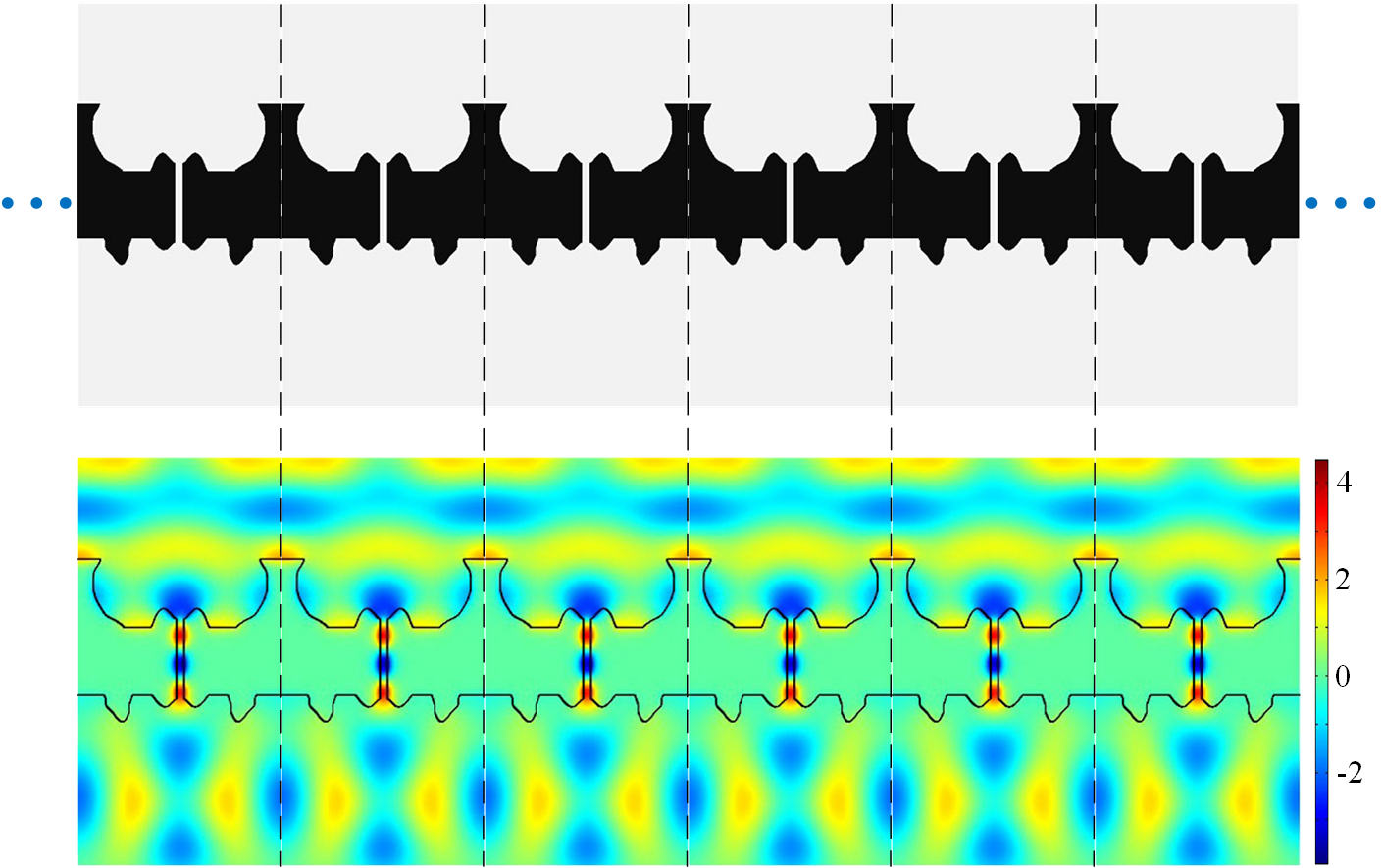
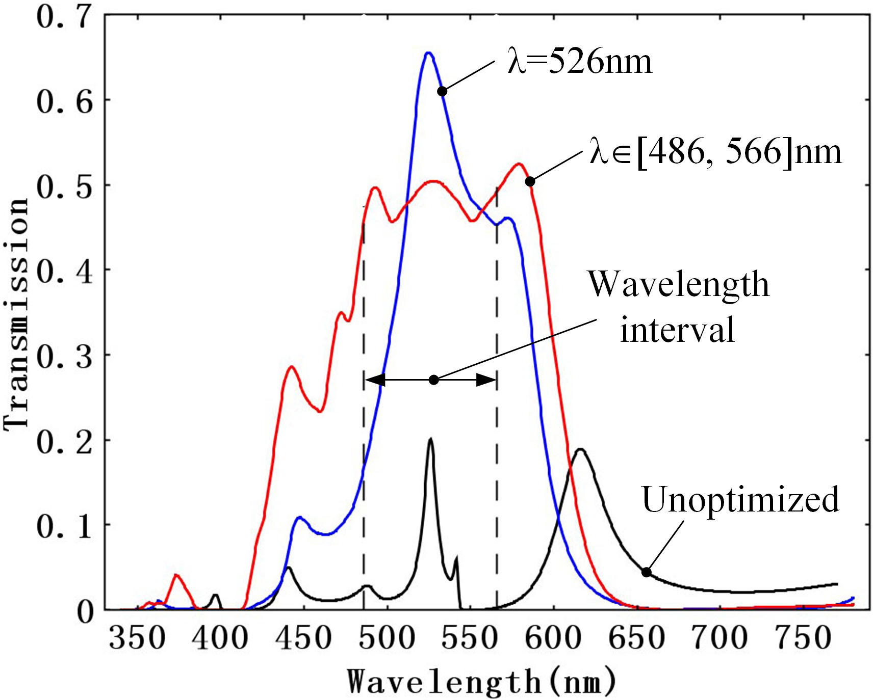
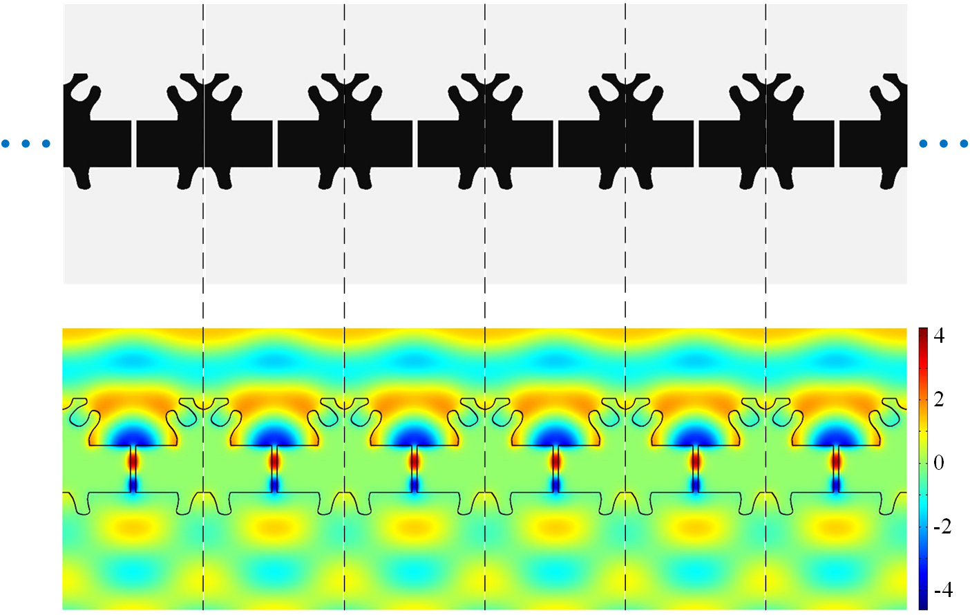
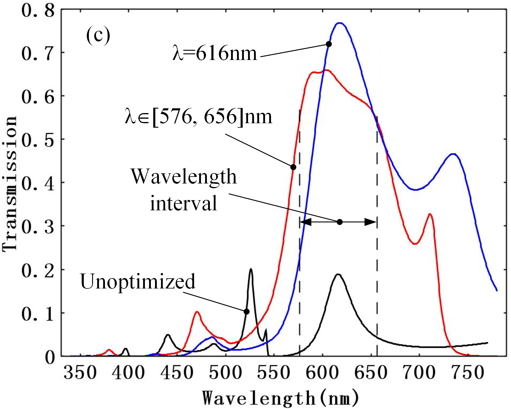
where is the central incident wavelength; is the support size of the wavelength perturbation range. By respectively setting the central incident wavelength and support size to be and nm, the geometrical configuration of the periodic metallic slits is derived as shown in Fig. 7a, where the magnetic field distribution corresponding to the minimum transmissivity at the wavelength nm is included; and the transmission spectra of the derived periodic metallic slits is shown in Fig. 7b. When the central incident wavelength is changed to be nm, the geometrical configuration shown in Fig. 8a is derived for the TM wave with incident wavelength in the range from to nm, where the magnetic field distribution corresponding to the minimum transmissivity at the wavelength nm is included; and the corresponding transmission spectra is shown in Fig. 8b. The transmission spectra in Fig. 7b and 8b, demonstrate that EOT is controlled to be less sensitive to the incident wavelength with the cost of decreasing transmissivity and it is feasible to enlarge the EOT bandwidth of subwavelength structures using the discussed inverse design method.
4 Conclusion
This paper has presented inversely determining the resonant configuration of the bilateral nanostructures for periodic metallic slits with extraordinary optical transmission performance. The topology optimization approach is utilized to implement the inverse design procedure. Several geometrical configurations of the bilateral nanostructures are derived for periodic metallic slits. The resonant performance of the derived nanostructures are demonstrated by the transmission spectra, where the transmission peak is presented at the specified wavelength in the inverse design procedure. This provides an approach to control the red or blue shift of the transmission peak or localize the resonant performance at a desired frequency, by specifying the desired incident wavelength in the inverse design procedure. The inverse design method is extended to make the periodic metallic slits to be less sensitive to the incident wavelength. This research can be further extended to inversely find the resonant subwavelength structures for extraordinary optical absorption and other surface palsmon polariton based photonic devices. The inverse design of three dimensional apertures for extraordinary optical transmission will be investigated in our future researches.
Acknowledgement
This work is supported by the National Natural Science Foundation of China (No. 51405465), the National High Technology Program of China (No. 2015AA042604), Science and Technology Development Plan of Jilin Province and Changchun City (No. 20170312027ZG, No. 15SS12).
References
- [1] T. W. Ebbesen, H. J. Lezec, H. F. Ghaemi, T. Thio, P. A. Wolff, “Extraordinary optical transmission through sub-wavelength hole arrays,” Nature 391, 667–669 (1998).
- [2] H. Liu, P. Lalanne, “Microscopic theory of the extraordinary optical transmission,” Nature 452, 728–731 (2008).
- [3] F. J. García de Abajo, “Light scattering by particle and hole arrays,” Reviews of Modern Physics 79, 1267–1290 (2007).
- [4] W. L. Barnes, A. Dereux , T. W. Ebbesen, “Surface plasmon subwavelength optics,” Nature 424, 824–830 (2003).
- [5] N. Engheta, “Circuits with light at nanoscales: Optical nanocircuits inspired by metamaterials,” Science 317, 1698–1702 (2007).
- [6] C. Genet, T. W. Ebbesen, “Light in tiny holes”, Nature 445, 39–46 (2007).
- [7] R. Gordon, D. Sinton, K. L. Kavanagh, A. G. Brolo, “A new generation of sensors based on extraordinary optical transmission,” Accounts of Chemical Research 41, 1049–1057 (2008).
- [8] T. Sødergaard, S. I. Bozhevolnyi, S. M. Novikov, J. Beermann, E. Devaux, T. W. Ebbesen, “Extraordinary optical transmission enhanced by nanofocusing,” Nano Lett. 10, 3123–3128 (2010).
- [9] H. Liu, T. Li, Q. J. Wang, Z. H. Zhu, S. M. Wang, J. Q. Li, S. N. Zhu, Y. Y. Zhu, X. Zhang, “Extraordinary optical transmission induced by excitation of a magnetic plasmon propagation mode in a diatomic chain of slit-hole resonators,” Physical Review B 79, 024304 (2009).
- [10] F. J. García-Vidal, H. J. Lezec, T.W. Ebbesen, L. Martín-Moreno, “Multiple paths to enhance optical transmission through a single subwavelength slit,” Physical Review Letters 90, 213901 (2003).
- [11] L. L. Wang, X. F. Ren, R. Yang, G. C. Guo, and G. P. Guo, “Transmission of doughnut light through a bulls eye structure,” Appl. Phys. Lett 95, 111111–111113 (2009).
- [12] Y. X. Cui, S. He, Y. Okuno, “Giant optical transmission through a metallic nanoslit achieved by the optimization of the groove periodicity and other parameters,” International Workshop on Metamaterials, 236–239 (2008).
- [13] E. Popov, M. Nevière, A. L. Fehrembach, N. Bonod, “Optimization of plasmon excitation at structured apertures,” Applied Optics 44, 6141–6154 (2005).
- [14] M. Bendsøe, “Optimal shape design as a material distribution problem,” Struct. Optim. 1, 193–202 (1989).
- [15] T. Borrvall, J. Petersson, “Topology optimization of fluids in Stokes flow,” Int. J. Numer. Methods Fluids 41, 77–107 (2003).
- [16] J. S. Jensen, O. Sigmund, “Topology optimization of photonic crystal structures: a high-bandwidth low-loss T-junction waveguide,” J. Opt. Soc. Am. B 22, 1191–1198 (2005).
- [17] M. Bendsøe, O. Sigmund, “Topology optimization-theory, methods and applications,” Springer, Berlin (2003).
- [18] A. Y. Piggott, J. Lu, K. G. Lagoudakis, J. Petykiewicz, T. M. Babinec, J. Vučović, “Inverse design and demonstration of a compact and broadband on-chip wavelength demultiplexer,” Nature Photonics 9, 374–377 (2015).
- [19] B. Shen, P. Wang, R. Polson, R. Menon, “An integrated-nanophotonics polarization beamsplitter with 2.42.4 m2 footprint,” Nature Photonics 9, 378–382 (2015).
- [20] L. H. Frandsen, Y. Elesin, L. F. Frellsen, M. Mitrovic, Y. Ding, O. Sigmund, K. Yvind, “Topology optimized mode conversion in a photonic crystal waveguide fabricated in silicon-on-insulator material,” Optics Express 22, 8525–8532 (2014).
- [21] O. Sigmund, K. G. Hougaard, “Geometric properties of optimal photonic crystals,” Phys. Rev. Lett. 100, 153904 (2008).
- [22] H. Men, K. Y. K. Lee, R. M. Freund, J. Peraire, S. G. Johnson, “Robust topology optimization of three-dimensional photonic-crystal band-gap structures” Optics Express 22(19), 22632–22648 (2014).
- [23] J. Andkjær, O. Sigmund, “Topology optimized low-contrast all-dielectric optical cloak,” Appl. Phys. Lett. 98, 021112 (2011).
- [24] B. Vial, Y. Hao, “Topology optimized all-dielectric cloak: design, performances and modal picture of the invisibility effect,” Optics Express 100, 23551–23560 (2015).
- [25] G. Fujii, H. Watanabe, T. Yamada, T. Ueta, M. Mizuno, “Level set based topology optimization for optical cloaks,” Appl. Phys. Lett. 102, 251106 (2013).
- [26] S. Zhou, W. Li, Y. Chen, G. Sun, Q. Li, “Topology optimization for negative permeability metamaterials using level-set algorithm,” Acta Materialia 59, 2624–2636 (2011).
- [27] A. R. Diaz, O. Sigmund, “A topology optimization method for design of negative permeability metamaterials,” Struct. Multidisc. Optim. 41, 163–177 (2010).
- [28] M. Otomori, T. Yamada, K. Izui, S. Nishiwaki, J. Andkjær, “A topology optimization method based on the level set method for the design of negative permeability dielectric metamaterials,” Comput. Methods Appl. Mech. Engrg. 237-240, 192–211 (2012).
- [29] J. Andkjær, S. Nishiwaki, T. Nomura, O. Sigmund, “Topology optimization of grating couplers for the efficient excitation of surface plasmons,” JOSA B 27, 1828–1832 (2010).
- [30] Y. Deng, Z. Liu, C. Song, P. Hao, Y. Wu, Y. Liu, J. G. Korvink, “Topology optimization of metal nanostructures for localized surface plasmon resonances,” Struct. Multidisc. Optim. DOI 10.1007/s00158-015-1388-8 (2015).
- [31] S. Zhou, W. Li, Q. Li, “Level-set based topology optimization for electromagnetic dipole antenna design,” Journal of Computational Physics 229, 6915–6930 (2010).
- [32] E. Hassan, E. Wadbro, M. Berggren, “Topology optimization of metallic antennas,” IEEE Transactions on Antennas And Propagations 62, 2488–2500 (2014).
- [33] T. Feichtner, O. Selig, M. Kiunke, B. Hecht, “Evolutionary optimization of optical antennas,” Phys. Rev. Lett. 109, 127701 (2012).
- [34] A. Erentok, O. Sigmund, “Topology optimization of sub-wavelength antennas,” IEEE Transactions on Antennas and Propagation 59, 58–69 (2011).
- [35] K. Svanberg, “The method of moving asymptotes-a new method for structural optimization,” Int. J. Numer. Methods Eng. 24, 359–373 (1987).
- [36] B. Lazarov, O. Sigmund, “Filters in topology optimization as a solution to Helmholtz type differential equations,” Int. J. Numer. Methods Eng. 86, 765–781 (2011).
- [37] F. Wang, B. S. Lazarov, O. Sigmund, “On projection methods, convergence and robust formulations in topology optimization,” Struct. Multidisc. Optim. 43, 767–784 (2011).
- [38] J. Guest, J. Prevost, T. Belytschko, “Achieving minimum length scale in topology optimization using nodal design variables and projection functions,” Int. J. Numer. Methods Eng. 61, 238–254 (2004).
- [39] O. Sigmund, “Morphology-based black and white filters for topology optimization,” Struct. Multidisc. Optim. 33, 401–424 (2007).
- [40] S. Xu, Y. Cai, G. Cheng, “Volume preserving nonlinear density filter based on heaviside funtions,” Struct. Multidisc. Optim. 41, 495–505 (2010).
- [41] A. Kawamoto, T. Matsumori, S. Yamasaki, T. Nomura, T. Kondoh, S. Nishiwaki, “Heaviside projection based topology optimization by a pde-filtered scalar function,” Struct. Multidisc. Optim. 44, 19–24 (2011).
- [42] M. Hinze, R. Pinnau, M. Ulbrich, S. Ulbrich, “Optimization with PDE Constraints,” Springer, Berlin (2009).
- [43] P. B. Johnson, R. W. Christy, “Optical Constants of the Noble Metals,” Phys. Rev. B 6, 4370–4379 (1972).
- [44] V. J. Sorger, R. F. Oulton, J. Yao, G. Bartal, X. Zhang, “Plasmonic Fabry-Pérot Nanocavity,” Nano Lett. 9-10, 3489–3493 (2009).
- [45] S. Astilean, P. Lalanne, M. Palamaru, “Light transmission through metallic channels much smaller than the wavelength,” Opt. Commun. 175, 265–273 (2000).
- [46] Y. Takakura, “Optical resonance in a narrow slit in a thick metallic screen,” Phys. Rev. Lett. 86, 5601–5603 (2001).
- [47] F. Yang, J. R. Sambles, “Resonant transmission of microwaves through a narrow metallic slit,” Phys. Rev. Lett. 89, 063901 (2002).
- [48] L. Cai, G. Li, Z. Wang, A. Xu, “Interference and horizontal Fabry-Pérot resonance on extraordinary transmission through a metallic nanoslit surrounded by grooves,” Optics Letters 35, 127–129 (2010).