Ferroelectric Control of Metal-Insulator Transition
Abstract
We propose a method of controlling the metal-insulator transition of one perovskite material at its interface with a another ferroelectric material based on first principle calculations. The operating principle is that the rotation of oxygen octahedra tuned by the ferroelectric polarization can modulate the superexchange interaction in this perovskite. We designed a tri-color superlattice of (BiFeO3)N/LaNiO3/LaTiO3, in which the BiFeO3 layers are ferroelectric, the LaNiO3 layer is the layer of which the electronic structure is to be tuned, and LaTiO3 layer is inserted to enhance the inversion asymmetry. By reversing the ferroelectric polarization in this structure, there is a metal-insulator transition of the LaNiO3 layer because of the changes of crystal field splitting of the Ni orbitals and the bandwidth of the Ni in-plane orbital. It is highly expected that a metal-transition can be realized by designing the structures at the interfaces for more materials.
keywords:
ferroelectric, bandwidth control , oxygen octahedron , metal-insulator transitionPACS 73.21.Ac , 77.55.Px , 73.20.At
1 Introduction
In transitional metal oxides,the strong correlation between lattice, charge, orbital, and spin leads to many novel properties. At their interfaces, even richer physics bring about emerging properties. Technical advances in the atomic-scale synthesis of oxide heterostructures make it possible for these interfaces to be artificially designed [1, 2, 3]. In perovskite oxide heterostructures where the oxygen octahedra share their vertices, the interplay among different distortion of octahedral units can dictate many novel functional properties [4]. One kind of interfaces between ferroelectric and other materials, of which the electronic properties are to be controlled, is very interesting because of the bi-stable property, with which two states can be reached by reversing the ferroelectric polarization with an electric field, with both changes from structure and from electric polarization involved. The controlling of the electronic structure can be through either the change of electric boundary condition [5], or structural distortion [6]. In this paper, we propose a strategy to control the electronic bandwidths and to achieve a metal-insulator transition in a material by stacking it onto a ferroelectric layer resulting in a modulation of structural distortion.
In this work, we use LaNiO3 as the electronic active material, of which the band gap is to be controlled. Nickelates, with the chemical formula RNiO3, have a prominent feature that there is a metal-insulator transition connected to the sizes of the R site ions by the rotation angles of octahedra [7]. The rotation of the octahedra can also be controlled by a strain, causing many works on the straining control of the electronic structure of nickelates such as in Refs. [8, 9, 10]. In addition, nickelate heterostructures have drawn great attentions since Chaloupka and Khaliullin proposed the possible superconductivity by modulating the orbitals [11]. With the proposed structure, the orbital occupations can also be tuned. We chose BiFeO3 as the ferroelectric material because of its large polarization. It has a relative small band gap, which enables it be used as semiconductor materials such as in switchable diodes[12, 13, 14, 15], therefore it is easier for charges to transfer from or to BiFeO3. One can make use of this effect to manipulate the charge transfer.
By stacking a ferroelectric and non-ferroelectric layers together, it is natural to think that the electronic properties can be tuned by reversing the ferroelectric polarization. While it is true for the asymmetric thin films, in a periodic superlattice, the structures of the two polarization states are the same (or very similar) by a 180 degree rotation if the two interfaces of a non-ferroelectric to the ferroelectric are the same (or very similar). For example, in a (BiFeO3)N/LaNiO3 superlattice, the two sides of LaNiO3 are the LaO and BiO planes. Since the La and Bi ions are close in radius and the same in valence states, large difference in electronic properties caused by reversing the polarization are not expected.
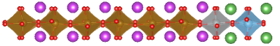
A method to enlarge the difference is to make the structure more asymmetric by inserting another layer. By inserting a LaTiO3 layer,tri-color superlattices of (BiFeO3)N/LaNiO3/LaTiO3 is formed as shown in Fig. 1. According to Chen, et al. [16], in LaTiO3, the Ti3+ ion has a electron with energy higher than that of the unoccupied Ni band in LaNiO3. Therefore electrons can transfer from Ti to Ni, forming a Ti and Ni configuration [17], so there is an electric polarization pointing from LaNiO3 to LaTiO3 at their interface. Thus the structures with opposite ferroelectric polarizations also differ in polarization continuity, which offers another way of controlling the electronic property by reversing the ferroelectric polarization. In the LaNiO3/LaTiO3 heterostructures, the crystal field splitting of the Ni orbitals is largely affected by the distortion of the oxygen octahedra caused by the polarity of the structure [16]. Thus the control of the ferroelectric polarization in the tri-color superlattice can also tune the electronic structure by influence the octahedra distortion.
2 Methods
We carried out first principle calculations to investigate the ferroelectric controlled metal-insulator transition in the superlattices. We set 6 layers of BiFeO3 in one supercell of (BiFeO3)N/LaNiO3/LaTiO3 (=6) in our models as shown in Fig. 1. The spontaneous polarization of the bulk BiFeO3 is along the [111] direction of the pseudo-cubic unit. With the compressive strain, the in-plane polarization tends to be suppressed so that the total polarization rotates towards [001]. When the in-plane lattice constant is about 3.71 Å, the BiFeO3 only films tend to transform to a “-like” phase with a large ratio about 1.2 to 1.3 and a large polarization approximately along [001] [18, 19]. However, in the (BiFeO3)6/LaNiO3/LaTiO3 structure, the cooperative shift of the Bi ions along the out-of-plane direction is impeded by the LaNiO3 and LaTiO3 layers. Thus, the BiFeO3 layers are in the “R-like” phase with the ratio of about 1.1 and the out-of-plane polarization of about 60 C/cm2, which is alike to the BiFeO3 films with in-plane lattice constants larger than 3.71 Å. Here we only make use of the out-of-plane component of the polarization, because the only change of the structure by reversing of the in-plane component is a rotation around the out-of-plane axis and there is no difference in the electronic structure. Therefore we refer the polarization to the out-of-plane component of it in this paper. We define the state which the ferroelectric polarization orientation pointing from LaNiO3 to LaTiO3 as +P, while the state with opposite polarization as -P. A pseudo-cubic in-plane lattice was used so that the oxygen octahedra can rotate freely. We kept the in-plane lattice parameters fixed as 3.71 Å, which is the LDA value of the substrate of LaAlO3, and relax all the other degrees of freedom of the structure. The G-type antiferromagnetic structure was found to be stable in the (BiFeO3)6/LaNiO3/LaTiO3 structure.
We performed the density functional theory (DFT) calculation based on the projected augmented wave [20] (PAW) and local spin density approximation (LSDA) [21] +Hubbard method [22] as implemented in the Vienna ab initio simulation package (VASP) [23]. The filled valence states include the orbitals , , , , , and for Bi, Fe, La, Ni, Ti, and O, respectively. A plane-wave basis set with energy cutoff of 500 eV and a -centered k-point grid were used. The structures were relaxed until the forces are less than 0.03 eV/Å. Though the LSDA + method cannot well describe the paramagnetic and insulating ground state in bulk LaTiO3 simultaneously, it can describe the LaNiO3/LaTiO3 structure [16]. Effective (Ni)=0 eV, (Ti)=4 eV, and (Fe)=6 eV are used throughout the work we presented here unless otherwise stated. The (Fe) is used only to make the band gap of BiFeO3 close to the experiment value. By following Ref. [16], (Ti)=4 eV was used to better align the Ti and Ni bands. We also found that (Ti) has no significant effect on the overall results, because the Ti bands are higher than the Ni bands and are thus almost empty no matter how large the (Ti) is. Disa et al. [24] used the (Ni) of 0 in a similar structure of LaAlO3/LaNiO3/LaTiO3 and they found good agreement with the experimental results. We also compared the results with a series of (Ni) ranging from 0 to 6 eV to see the effect of the Coulomb repulsion.
Two sets of Maximally localized Wannier functions (MLWFs) [25] were constructed to investigate the mechanism of the metal-insulator transition using the Wannier90 package and its interface to VASP [26]. The first set of MLWFs is band only, each function is of hybridized transitional metal orbital and the neighboring O feature. The other set of WLWFs, which is constructed to calculate the layer resolved polarization, consists of all the occupied-orbital-like wave functions.
3 Results and Discussion
In the (BiFeO3)N/LaNiO3/LaTiO3 structure, the bands near the Fermi energy are bands of Ni. We first look into the local structural distortions near the LaNiO3 layer as shown in Fig. 2. The charge transfer between the LaTiO3 and LaNiO3 stays the same as in LaNiO3/LaTiO3 superlattices. La ions between NiO and TiO planes move towards the NiO plane to compensate the dipoles caused by the charge transfer. Bi ions at the BiFeO3/LaNiO3 interface shift away from the NiO plane in the -P state because of the ferroelectric polarization, while they shift towards the Ni-O plane in the +P state. As compared to the +P state, the distances between the Bi and La ions are larger in the -P state, and the diagonals of the oxygen octahedra along the out-of-plane direction in the frame of Bi and La ions are also longer; the in-plane Ni-O bond lengths are reduced from about 1.90 Å in the +P state to about 1.88 Å in the -P state to compensate the increasing of the volume of the oxygen octahedra caused by the elongation in the out-of-plane direction. Relative to the +P state, the larger Jahn-Teller distortion of the octahdron shifts the energy of the Ni orbital up and that of the Ni orbital down in the -P state. Thus, the band gaps of the +P and -P states are different.
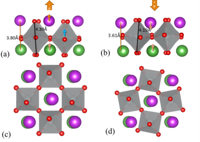
The shorter in-plane Ni-O bonds in the -P state requires the Ni-O-Ni bond angles to be increased to accommodate the lattice constant fixed to the substrate.The details of the distortion and rotation patterns of the Ni-O octahedra are shown in Fig. 2. In the -P state, the rotations of the octahdedra are suppressed with the rotation angles less than 1∘. The directions of the ferroelectric polarization and the polarization caused by the LaNiO3/LaTiO3 charge transfer are opposite, leading to a polar discontinuity as shown in Fig. 4. The Ni ions shift relative to the O ions to compensate the polar discontinuity, thus the the O-Ni-O bond angles along the x (or y) direction are about 164∘ in the Ni-O octahedra. The oxygen octahedra in the tri-color superlattice rotate and tilt with the pattern in Glazer notation[27]. The oxygen octahedra tilt clockwise and anticlockwise alternately, with the tilting angles about 8∘. So the Ni-O octahedra in a chain are connected in clockwise-anticlockwise and anticlockwise-clockwise mode alternately. This shifting of Ni ions increase the Ni-O-Ni bond angles at the clockwise-anticlockwise connection, while decrease the angle at the anticlockwise-clockwise connection. Therefore, there are two kinds of Ni-O-Ni bond angles about 173∘ and 157∘, respectively. In the +P state, the rotation (with the angle about 10∘) and tilting (with the angle about 6∘) of the octahedra are the predominant distortion patterns, which make the Ni-O-Ni bond angles about 157∘.
The Ni-O-Ni bond angles are larger in the -P state, thus the overlapping of the Ni and the O orbitals is larger. What we can expect from this is a wider bandwidth and hopefully a metal-insulator transition.
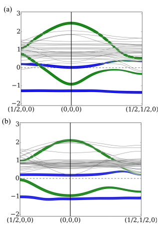
We calculated the band structure for the both the -P and +P states. The +P state has a band gap of about 0.2 eV, whereas the -P state is metallic. To see the detail of the change of the band structure, we constructed MLWFs and extracted an effective band only tight-binding Hamiltonian with the MLWFs as the basis set. Thus the MLWFs are of hybrid features. The band structure were calculated with this Hamiltonian, with one of the two spin channels (spin up) shown in Fig.3. The band structure of the other spin channel is the same because the structure is antiferromagnetic. The two Ni atoms in the calculated supercell with total spin up and down are denoted as Ni1 and Ni2 here, respectively. The two spin up states of Ni1 have lower energies than those of Ni2. The projection of the eigenstates to the Ni bands are shown. The four bands with spin up of the two Ni atoms are near the Fermi energies. It can be clearly seen that the metal-insulator transition is related to the change of the Ni bandwidths. The bands are flat because the bands in the out-of-plane direction are confined. Whereas the in-plane bands can be seen as the bonding and antibonding states of the two Ni in-plane orbitals. The width of the band is proportional to the hopping integral . In the -P state, the hopping integrals are -0.41 eV and -0.36 eV corresponding to the Ni-O-Ni bonds with the angles 173∘ and 157∘, respectively. While in the +P state, the hopping integral is -0.37 eV corresponding to the Ni-O-Ni bonds with the angles 157∘. It can be seen that the rule is well fitted. Therefore, the change of the bandwidths can be attributed to the structural distortion.
| -P | -1.22 | 0.53 | 0.16 | 0.94 |
| +P | -1.08 | -0.15 | 0.16 | 0.8 |
The relative shift of the Ni bands also largely affect the band gap. The on-site energies of the Wannier functions are listed in table 1. In the -P state, the crystal field splitting is larger than that that in the -P state, as the oxygen ocataheras are more elongated in the direction. Consequently, the on-site energy of of Ni1 is raised even higher than that of the of Ni2, leading to the crossover of the corresponding and bands.
We examined the possible effect of electron repulsion by adding an effective Hubbard ranging from 0 to 6 eV. The Hubbard pushes the occupied bands down and the unoccupied bands up, which inhibits the crossing over of these bands and the metallic state. With of above 4 eV, the metal-insulator transition is absent. Whether the metallic state can survive still needs experimental tests and better theoretical descriptions of the electron correlation effect. Nevertheless, the control of the bandwidths and band gap should be robust.
It should be noted that the carrier localization effect sometimes plays a role in 2D thin film structures, which make the structure with zero gap behave like insulators, like in Refs. [28, 29]. We cannot rule out the possibility within our DFT calculation. Even so, a change in the conducting mechanism should be still observable.
From Fig. 3, the Ni a few Fe bands at the BiFeO3/LaTiO3 interface cross the Fermi energy, showing a transfer of electrons from the LaNiO3 to the BiFeO3 layers. This can be understood as the result as the polarization discontinuity. The charge transfer from the LaTiO3 to the LaNiO3 layer caused a polarization pointing from LaNiO3 to LaTiO3, the orientation of which is the same as the ferroelectric polarization of BiFeO3 in the +P state, while is different in the structure of -P. Though partly compensated by structural relaxation, the discontinuity can still lead to the charge transfer.
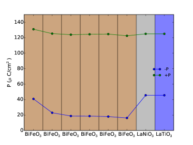
We calculated the layer resolved polarization following the method of Stengel et al. by constructing maximally localized Wannier functions [30, 31]. The six Ni and two electrons with majority spin, the five Fe electrons in the majority spin channel, the O electrons, and all the electrons at lower energies were considered as bounded charge. The charge neutral condition is not satisfied in the LaNiO3 and LaTiO3 layers because of the charge transfer between them. Therefore, we considered them as a whole and calculated the averaged polarization. As shown in Fig. 4, the polarizations are almost unified in the +P state, whereas the polarization discontinuity exists at both the BiFeO3 interfaces in the -P state. According to the Polarization continuity condition , the charge transfer from the LaNiO3 layer to the BiFeO3 layers. It should be noted that the polarizations in Fig. 4 are the formal polarization[30], not the effective polarization which is commonly used to describe the spontaneous ferroelectric polarization. In the A3+B3+O perovskite structures, due to the (AO)+(BO2)- alignment, there is a component of the formal polarization of about (about 70 C/cm2 in the BiFeO3 layers), where is the electron charge, is the lattice constant along the out-of-plane direction of the pseudocubic, and is the volume of the volume of the pseudocubic. By subtracting it from the formal polarizations, the residuals (which are approximately the effective polarizations) in the BiFeO3 layers are about +60 C/cm2 and -50 C/cm2 in the +P and -P states respectively.
We also calculated the band alignment of each layer, as shown in Fig. 5. The polarization discontinuity causes the band shift in the BiFeO3 in the -P state, whereas the much smaller polarization discontinuity causes almost no shift in the +P state. The result corroborated the charge transfer caused by the polarization discontinuity in -P state.
With the relative shift and the change of the width of the bands controlled by the reversing of the ferroelectric polarization, the Ni orbital polarization can also be modulated. The orbital polarization can be written as , where and are the occupations of the and orbitals, respectively, as opposite to that defined in Refs. [32, 33]. From Fig. 3, we can clearly see part of band which is beneath the Fermi energy in the +P state goes above the Fermi energy. is 0.41 and 0.12 in the +P and -P state.
The magnetic properties of the LaNiO3 can also be tuned. Because of the charge transfer and possibly the change of electron correlation effect which is related to the bandwidth, the local spin on Ni site is also tuned. In the -P state, the net spin projected on the Ni site is 0.66 , while that in the +P state is 1.05 .
4 Conclusion
In this work, we propose a strategy to control the electronic bandwidths and the band gap of a material stacked on the ferroelectric layer by reversing the ferroelectric polarization. This strategy is demonstrated to be feasible by designing a (BiFeO3)N/LaNiO3/LaTiO3 superlattice based on first principle calculations. The lattice distortion pattern changes with the orientation of the polarization. The on-site energies of the Ni orbitals related to the Jahn-Teller distortion of the Ni-O octahedron, and the widths of the in-plane Ni bands related the oxygen octahedron rotation angles and Ni-O-Ni bond angles, can both be thus be controlled by the reversing of the ferroelectric polarization. We also found the possibility of tuning of charge transfer between LaNiO3 layers and the BiFeO3 layers due to the change of polarization discontinuity condition. The orbital polarization and local Ni magnetic moment can also be manipulated.
Acknowledgement
The authors thank Jian-di Zhang for useful discussion. The work was supported by the National Basic Research Program of China (No. 2014CB921001), the National High Technology Research and Development Program of China (No. 2014AA032607), the National Natural Science Foundation of China (Nos. 11134012, 11404380, and 11474349), and the Strategic Priority Research Program (B) of the Chinese Academy of Sciences (No. XDB07030200).
References
- Mannhart and Schlom [2010] J. Mannhart and D. G. Schlom, Science 327, 1607 (2010).
- Hwang et al. [2012] H. Hwang, Y. Iwasa, M. Kawasaki, B. Keimer, N. Nagaosa, and Y. Tokura, Nat. Mater. 11, 103 (2012).
- Chakhalian et al. [2014] J. Chakhalian, J. W. Freeland, A. J. Millis, C. Panagopoulos, and J. M. Rondinelli, Rev. Mod. Phys. 86, 1189 (2014).
- Rondinelli et al. [2012] J. M. Rondinelli, S. J. May, and J. W. Freeland, MRS Bulletin 37, 261 (2012).
- Zubko et al. [2011] P. Zubko, S. Gariglio, M. Gabay, P. Ghosez, and J.-M. Triscone, Annu. Rev. Condens. Matter Phys. 2, 141 (2011).
- Borisevich et al. [2010] A. Y. Borisevich, H. J. Chang, M. Huijben, M. P. Oxley, S. Okamoto, M. K. Niranjan, J. D. Burton, E. Y. Tsymbal, Y. H. Chu, P. Yu, R. Ramesh, S. V. Kalinin, and S. J. Pennycook, Phys. Rev. Lett. 105, 087204 (2010).
- Medarde [1997] M. L. Medarde, J. Phys.: Condens. Matter 9, 1679 (1997).
- May et al. [2010] S. J. May, J.-W. Kim, J. M. Rondinelli, E. Karapetrova, N. A. Spaldin, A. Bhattacharya, and P. J. Ryan, Phys. Rev. B 82, 014110 (2010).
- Bruno et al. [2013] F. Y. Bruno, K. Z. Rushchanskii, S. Valencia, Y. Dumont, C. Carrétéro, E. Jacquet, R. Abrudan, S. Blügel, M. Ležaić, M. Bibes, and A. Barthélémy, Phys. Rev. B 88, 195108 (2013).
- Hwang et al. [2013] J. Hwang, J. Son, J. Y. Zhang, A. Janotti, C. G. Van de Walle, and S. Stemmer, Phys. Rev. B 87, 060101 (2013).
- Chaloupka and Khaliullin [2008] J. c. v. Chaloupka and G. Khaliullin, Phys. Rev. Lett. 100, 016404 (2008).
- Choi et al. [2009] T. Choi, S. Lee, Y. Choi, V. Kiryukhin, and S.-W. Cheong, Science 324, 63 (2009).
- Jiang et al. [2011] A. Q. Jiang, C. Wang, K. J. Jin, X. B. Liu, J. F. Scott, C. S. Hwang, T. A. Tang, H. Bin Lu, and G. Z. Yang, Adv. Matter. 23, 1277+ (2011).
- Wang et al. [2011] C. Wang, K. Jin, Z. Xu, L. Wang, C. Ge, H. Lu, H. Guo, M. He, and G. Yang, Appl. Phys. Lett. 98, 192901 (2011).
- Ge et al. [2011] C. Ge, K. Jin, C. Wang, H. Lu, C. Wang, and G. Yang, Appl. Phys. Lett. 99, 063509 (2011).
- Chen et al. [2013] H. Chen, D. P. Kumah, A. S. Disa, F. J. Walker, C. H. Ahn, and S. Ismail-Beigi, Phys. Rev. Lett. 110, 186402 (2013).
- Karolak et al. [2015] M. Karolak, M. Edelmann, and G. Sangiovanni, Phys. Rev. B 91, 075108 (2015).
- Béa et al. [2009] H. Béa, B. Dupé, S. Fusil, R. Mattana, E. Jacquet, B. Warot-Fonrose, F. Wilhelm, A. Rogalev, S. Petit, V. Cros, A. Anane, F. Petroff, K. Bouzehouane, G. Geneste, B. Dkhil, S. Lisenkov, I. Ponomareva, L. Bellaiche, M. Bibes, and A. Barthélémy, Phys. Rev. Lett. 102, 217603 (2009).
- Hatt et al. [2010] A. J. Hatt, N. A. Spaldin, and C. Ederer, Phys. Rev. B 81, 054109 (2010).
- Kresse and Joubert [1999] G. Kresse and D. Joubert, Phys. Rev. B 59, 1758 (1999).
- Perdew and Zunger [1981] J. P. Perdew and A. Zunger, Phys. Rev. B 23, 5048 (1981).
- Dudarev et al. [1998] S. Dudarev, G. Botton, S. Savrasov, C. Humphreys, and A. Sutton, Phys. Rev. B 57, 1505 (1998).
- Kresse and Furthmüller [1996] G. Kresse and J. Furthmüller, Phys. Rev. B 54, 11169 (1996).
- Disa et al. [2015] A. S. Disa, D. P. Kumah, A. Malashevich, H. Chen, D. A. Arena, E. D. Specht, S. Ismail-Beigi, F. Walker, and C. H. Ahn, Phys. Rev. Lett. 114, 026801 (2015).
- Mostofi et al. [2008] A. A. Mostofi, J. R. Yates, Y.-S. Lee, I. Souza, D. Vanderbilt, and N. Marzari, Comput. Phys. Commun. 178, 685 (2008).
- Franchini et al. [2012] C. Franchini, R. Kováčik, M. Marsman, S. S. Murthy, J. He, C. Ederer, and G. Kresse, J. Phys.: Condens. Matter 24, 235602 (2012).
- Glazer [1972] A. M. Glazer, Acta Crystallographica Section B 28, 3384 (1972).
- Sakai et al. [2013] E. Sakai, M. Tamamitsu, K. Yoshimatsu, S. Okamoto, K. Horiba, M. Oshima, and H. Kumigashira, Phys. Rev. B 87, 075132 (2013).
- Scherwitzl et al. [2011] R. Scherwitzl, S. Gariglio, M. Gabay, P. Zubko, M. Gibert, and J.-M. Triscone, Phys. Rev. Lett. 106, 246403 (2011).
- Stengel and Vanderbilt [2009] M. Stengel and D. Vanderbilt, Phys. Rev. B 80, 241103 (2009).
- Stengel et al. [2011] M. Stengel, P. Aguado-Puente, N. A. Spaldin, and J. Junquera, Phys. Rev. B 83, 235112 (2011).
- Han et al. [2010] M. J. Han, C. A. Marianetti, and A. J. Millis, Phys. Rev. B 82, 134408 (2010).
- Han et al. [2011] M. J. Han, X. Wang, C. A. Marianetti, and A. J. Millis, Phys. Rev. Lett. 107, 206804 (2011).