Scaling like behaviour of resistivity observed in thin films grown on substrate by pulsed laser deposition
Abstract
We discuss the origin of the temperature dependence of resistivity observed in highly oriented thin films grown on substrate by a pulsed laser deposition technique. All the experimental data are found to collapse into a single universal curve for the entire temperature interval () with being the onset temperature for triggering a resonant scattering of conduction electrons by spin fluctuations in heterostructure.
pacs:
71.20.Be, 71.30.+h, 73.20.-r, 73.50.-hKeywords: nickelates, thin films, size effects, resistivity, spin fluctuations, scaling
1 Introduction
Recently, ferroelectric thin films have rekindled discussion about their potential applications in non-volatile random memory and microsensors devices [1-4]. Of special interest are (LNO) based materials [5,6] which exhibit properties quite different from the other members of the nickelates family ( being a rare-earth element). Namely, LNO does not undergo a metal-insulator transition (MIT) from paramagnetic metal to antiferromagnetic insulator. Recall that LNO has the perovskite structure with the pseudo-cubic lattice parameter and when it is manufactured in the form of thin films it has a rather good compatibility with oxide substrates typically used for deposition, such as (STO) and (LAO), important for applications in ferroelectric FE-RAM.
Based on the substrate properties and intrinsically induced strain in film/substrate heterostructure, it was found [7-10] that magnetic and transport characteristics of deposited LNO films could be drastically changed. More specifically, a partial suppression of the charge ordering (responsible for MIT in nickelates) can be achieved by simply changing the film thickness which leads to formation of a principally new magnetic structure, the so-called pure spin-density wave (SDW) material, exhibiting properties of an antiferromagnetic metal [11-16] (with Neel temperatures ). Besides, an important influence of both composition and strain on the electrical properties of LNO thin films has been reported [17].
This work reports on the successful preparation, characterization and transport measurements of highly -oriented LNO thin films grown on oriented STO substrates by using pulsed laser deposition (PLD) technique. All the obtained resistivity data (as a function of temperature and film thickness) for three different films are found to collapse into a universal curve, exhibiting a scaling like behaviour dominated by conduction electrons scattering on spin fluctuations (supported by formation of SDW within heterostructure interface) for the entire temperature interval.
2 Experimental methods
In order to provide high quality samples (with atomically smooth surfaces compatible with that of the target at a wide range of oxygen pressure), PLD technique was used to deposit thin films of LNO on oriented STO substrate with typical dimensions of . Laser wavelength and repetition rate were ( laser with pulse duration) and , respectively. The laser energy was maintained constant during the deposition and the beam was focused on the ceramic targets by a quartz lens to a fluency of around for all the samples. During ablation, the target was rotated () in order to reduce non uniform erosion and to get the films as homogeneous as possible. The heater power was monitored by a computer during the increase and decrease of the temperature. The temperature during deposition was measured by a thermocouple in contact with the heater and the bottom (back side) of the substrate. The substrate was placed parallel to the target and the distance between them was around which was the best distance found due to the length of the plume. Before deposition, the base pressure of was applied and then the substrates were heated at for to get a carbon free and high crystalline surface. Deposition temperature for all films was defined as under a flowing oxygen pressure of maintained by a computerized mass flow controller to SCCM (standard cubic centimetres per minute). After the deposition, the samples were in situ annealed at the same temperature for under oxygen pressure to improve the quality of films and decrease the oxygen vacancy. The dense and crack-free LNO ceramic circular target with diameter of and thickness of was prepared from highly pure polymeric precursors by Pechini method [18] using ( Aldrich) and ( Aldrich). Calcination and sintering were performed in the air at for and at for , respectively. The target was polished after every film deposition to ensure comparable deposition conditions, especially the deposition rate. After that, the pre-ablation process was carried out for to prevent the deposition of the weakly bonded particles.
The electrical resistivity was measured using the conventional four-probe method. To avoid Joule and Peltier effects, a dc current was injected (as a one second pulse) successively on both sides of the sample. The voltage drop across the sample was measured with high accuracy by a nanovoltmeter.
3 Results and discussion
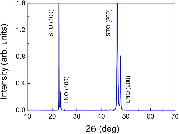
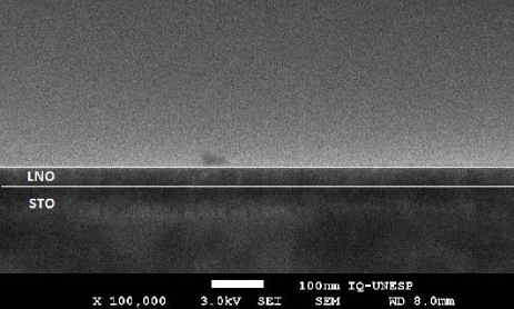
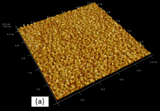
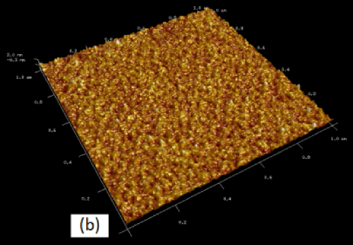
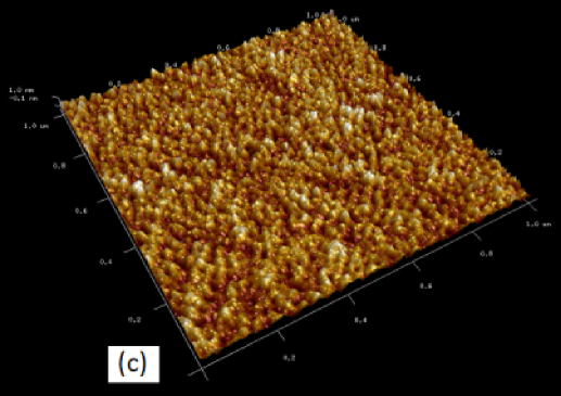
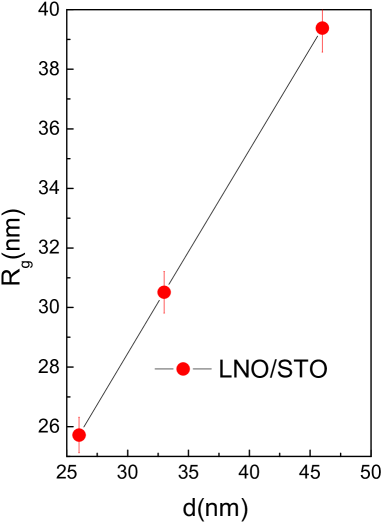
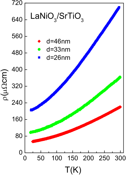
Microstructure and crystallographic orientation of the films were characterized by X-ray diffraction (XRD) scans. The surface morphology was studied by atomic force microscopy (AFM) and films thickness was confirmed by using field-emission scanning electron microscopy (FEG SEM). Typical XRD spectra and FEG SEM images for the thickest LNO films deposited on STO substrate are shown in Fig.1 and Fig.2, respectively. AFM scans of LNO/STO hybrid structures (for three LNO films with thickness of , and ) are depicted in Fig.3. Fig.4 shows the deduced from AFM scans relation between film thickness and the grain size . The results show that for the thinnest films this relation is practically linear. Fig.5 shows the typical results for the temperature dependence of the resistivity in our thin films heterostructure.
Given the above discussion on appearance of magnetic order in LNO/STO hybrid structure, it is quite reasonable to assume that the observed temperature behaviour of resistivity can be attributed to the manifestation of strong long-range spin fluctuations with a characteristic energy corresponding to low-energy spin dynamics spectrum measured by inelastic neutron scattering experiments. It should be pointed out that a rather significant scattering of conduction electrons by spin fluctuations is well documented for many different materials, see, e.g., [19-26] and further references therein. Recently, we suggested a simple phenomenological model based on the resonant like features of SDW type spectrum which result in the observed universal temperature dependence of the resistivity, see [27] for more discussion.
| (1) |
where is the total residual resistivity and is the onset temperature at which spin fluctuations begin to dominate the scattering process in our thin films heterostructure.
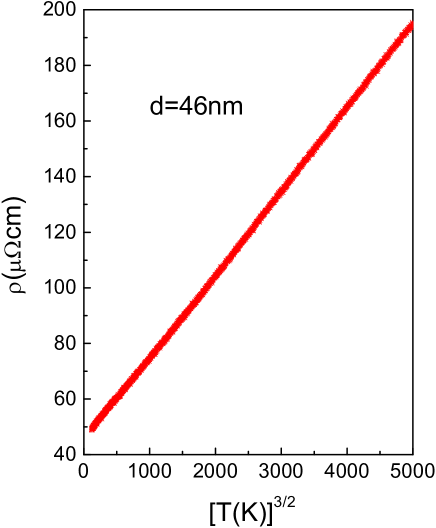
Fig.6 shows the best fit of the resistivity data for the thickest film (with ) according to Eq.(1) with , and . The latter corresponds to in the inelastic neutron scattering spectrum due to antiferromagnetic spin fluctuations [21,27].
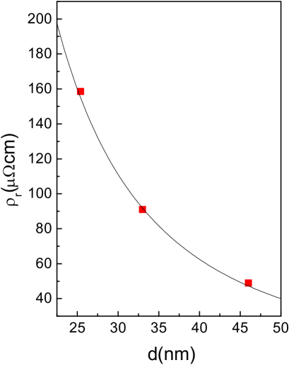
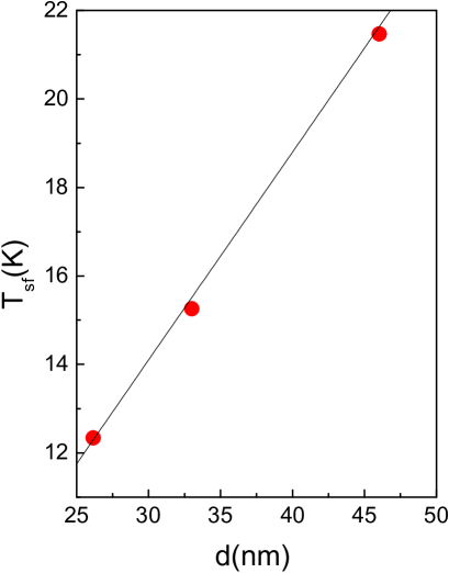
Now, using equation (1), we can deduce the dependence of the residual resistivity and of the onset spin-fluctuation temperature on film thickness . The obtained results are presented in Fig.7 and Fig.8, respectively. Recall that within the free electron gas model, is related to the electron density as . Thus, expectedly, according to Fig.7, the electron density increases with increasing the film thickness. On the other hand, according to Fig.8, the thinner is the film, the lower is the spin fluctuations onset temperature triggering the scattering processes in our films.
Based on the deduced information about and , we are able now to fit all the data for all the films by assuming a simple scaling like temperature behaviour of the normalized resistivity as a function of the reduced temperature where
| (2) |
and
| (3) |
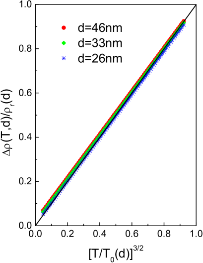
Fig.9 is the main result of this paper. As we can see, all the data points (for all temperatures and all films) collapse nicely into a single line fitted (solid line) by Eqs.(1)-(3).
And finally, to justify the universality of the observed behaviour over the entire measured temperatures, it was suggested [20,27] that the resonant scattering of conducting electrons by intraband spin fluctuations replenishes the electron distribution (depleted by interband inelastic scattering) while having a little effect on the current, thus making intraband scattering mechanism responsible for the robustness of the behaviour in intrinsically strained thin films based heterostructure.
4 Conclusion
In summary, by analysing the temperature dependence of the resistivity for three different thin films grown on oriented substrate (using a pulsed laser deposition technique) we were able to successfully fit all the experimental data by assuming a universal film thickness dependent scaling like law dominated by resonant scattering of conducting electrons on spin fluctuations supported by spin-density wave propagation through the interface boundary of heterostructure.
References
References
- [1] Ramesh R and Schlom D G 2002 Science 296 1975
- [2] Bhardwaj A, Burbure N V and Rohrer G S 2010 J.of American Ceramic Soc. 93 4129
- [3] Fu C et al 2010 J. of Electronic Materials 39 258
- [4] Liao J et al 2012 Materials Chemistry and Physics 135 1030
- [5] Ge J et al 2013 Appl. Phys. Lett. 102 142905
- [6] Pontes D S L, Pontes F M, Pereira-da-Silva Marcelo A, Berengue O M, Chiquito A J and Longo E 2013 Ceramics International 39 8025
- [7] Freeland J W, Liu Jian, Kareev M, Gray B, Kim J W, Ryan P, Pentcheva R and Chakhalian J 2011 Europhys. Lett. 96 57004
- [8] Han M J, Wang X, Marianetti C A and Millis A J 2011 Phys. Rev. Lett. 107 206804
- [9] Scherwitzl R, Gariglio S, Gabay M, Zubko P, Gibert M and Triscone J-M 2011 Phys. Rev. Lett. 106 246403
- [10] Liu Jian, Okamoto S, van Veenendaal M, Kareev M, Gray B, Ryan P, Freeland J W and Chakhalian J 2011 Phys. Rev. B 83 161102
- [11] Lee S B, Chen R and Balents L 2011 Phys. Rev. Lett. 106 016405
- [12] Frano A 2014 Spin Spirals and Charge Textures in Transition-Metal-Oxide Heterostructures (Springer Theses, Switzerland), Chapter 3
- [13] Sakai Enju, Tamamitsu Masatomo, Yoshimatsu Kohei, Okamoto Satoshi, Horiba Koji, Oshima Masaharu and Kumigashira Hiroshi 2013 Phys. Rev. B 87 075132
- [14] Zhu Mingwei, Komissinskiy Philipp, Radetinac Aldin, Wang Zhanjie and Alff Lambert 2015 J. Appl. Phys. 117 155306
- [15] Boris A V et al 2011 Science 332 937
- [16] Detemple E et al 2011 Appl. Phys. Lett. 99 2119031
- [17] Zhu Mingwei, Komissinskiy Philipp, Radetinac Aldin, Vafaee Mehran, Wang Zhanjie and Alff Lambert 2013 Appl. Phys. Lett. 103 141902
- [18] Pechini M 1967 US Patent no. 3.330.697
- [19] Rosch A 2000 Phys. Rev. B 62 4945
- [20] Smith M F 2006 Phys. Rev. B 74 172403
- [21] Sergeenkov S, Lanfredi A J C and Araujo-Moreira F M 2007 JETP Lett. 85 592
- [22] Mansuri Irfan and Varshney Dinesh 2012 Journal of Alloys and Compounds 513 256
- [23] Choudhary K K 2012 Journal of Physics and Chemistry of Solids 73 460
- [24] Varshney Dinesh, Mansuri Irfan, Shaikh M W and Kuo Y K 2013 Materials Research Bulletin 48 4606
- [25] Choudhary K K 2015 Int. J. Nanoscience 14 1550010
- [26] Shaikh M W, Mansuri Irfan, Dar M A and Varshney Dinesh 2015 Materials Science in Semiconductor Processing 35 10
- [27] Sergeenkov S, Cichetto L Jr, Longo E and Araujo-Moreira F M 2015 JETP Lett. 102 383