Resonant tunneling and the quasiparticle lifetime in graphene/boron nitride/graphene heterostructures
Abstract
Tunneling of quasiparticles between two nearly-aligned graphene sheets produces resonant current-voltage characteristics because of the quasi-exact conservation of in-plane momentum. We claim that, in this regime, vertical transport in graphene/boron nitride/graphene heterostructures carries precious information on electron-electron interactions and the quasiparticle spectral function of the two-dimensional electron system in graphene. We present extensive microscopic calculations of the tunneling spectra with the inclusion of quasiparticle lifetime effects and elucidate the range of parameters (inter-layer bias, temperature, twist angle, and gate voltage) under which electron-electron interaction physics emerges.
I Introduction
The quantum lifetime mahan_book_1981 of electrons roaming in semiconductors and semimetals is the result of microscopic scattering events between electrons and disorder, lattice vibrations, and other electrons in the Fermi sea.
At low temperatures, the lifetime of electrons close to the Fermi surface is dominated by elastic scattering off of the static disorder potential in the material. Upon increasing temperature, however, inelastic scattering mechanisms like electron-phonon and electron-electron (e-e) scattering begin to play a role. Standard electrical transport measurements are sensitive to elastic scattering and electron-phonon processes. The e-e scattering time , which in a normal Fermi liquid coincides with the quasiparticle lifetime Nozieres ; Pines_and_Nozieres ; Giuliani_and_Vignale , is much harder to extract from dc transport since such e-e scattering processes conserve the total momentum of the electron system. At low temperatures, order-of-magnitude estimates of are often obtained from weak localization measurements altshuler_jpc_1982 ; imry_sst_1994 of the dephasing time .
Direct measurements of are however possible. Any experiment that accesses the so-called quasiparticle spectral function Nozieres ; Pines_and_Nozieres ; Giuliani_and_Vignale , is sensitive to . (Here, , , and denote wave vector, energy, and chemical potential, respectively.) It is well known that angle-resolved photoemission spectroscopy (ARPES) damascelli_rmp_2003 is one of such experiments. In the case of graphene, accurate ARPES measurements bostwick_naturephys_2007 ; zhou_naturemater_2007 ; bostwick_science_2010 ; walter_prb_2011 ; siegel_pnas_2011 of require large flakes and have therefore been limited to high-quality epitaxial samples grown on the silicon or carbon face of SiC.
What is less known is that tunneling between two two-dimensional (2D) electron systems murphy_prb_1995 ; Giuliani_and_Vignale with simultaneous conservation of energy and momentum also probes and therefore . In these experiments, the tunnel current flowing perpendicularly between two parallel 2D electron systems separated by a barrier is measured. The conservation of in-plane momentum strongly constrains the phase space for tunneling processes and grants unique access to the quasiparticle spectral function . 2D-to-2D tunneling spectroscopy was carried out by Murphy al. murphy_prb_1995 on double quantum well heterostructures consisting of two GaAs quantum wells separated by an undoped barrier with a width in the range . Experimental results for the width of the tunneling resonances were compared with available theoretical results on the quasiparticle lifetime of a 2D parabolic-band electron system chaplik_jetp_1971 ; hodges_prb_1971 ; fukuyama_prb_1983 ; giuliani_prb_1982 and stimulated much more theoretical work jungwirth_prb_1996 ; zheng_prb_1996 ; reizer_prb_1997 ; marinescu_prb_2002 ; qian_prb_2005 .
Recently, a large number of 2D-to-2D tunneling spectroscopy experiments has been carried out in van der Waals heterostructures geim_nature_2013 comprising two graphene sheets separated by a hexagonal boron nitride (hBN) barrier britnell_nanolett_2012 ; britnell_science_2012 ; britnell_naturecommun_2013 ; mishchenko_naturenano_2014 . In particular, this work is motivated by the recently gained ability to align the two graphene crystals britnell_naturecommun_2013 ; mishchenko_naturenano_2014 ; fallahazad_nanolett_2015 , which enables tunneling measurements in which the in-plane momentum is nearly exactly conserved. Here, we present a theoretical analysis of the role of intra-layer e-e interactions on the tunneling characteristics of graphene/hBN/graphene heterostructures as sketched in Fig. 1. To the best of our knowledge, all available theoretical studies feenstra_jourapplphys_2012 ; delabarrera_jvactechnol_2014 ; brey_prapp_2014 ; wallbank_thesis_2014 ; mishchenko_naturenano_2014 ; lane_apl_2015 of tunneling in these heterostructures have not dealt with e-e interaction effects.
Our Article is organized as following. In Sect. II we present the tunneling Hamiltonian and an expression for the tunneling current as a functional of the quasiparticle spectral function for conduction- () and valence-band () states in each layer. In Sect. III we present two crucial ingredients for the calculation of the tunneling current: i) electrostatic relations linking the chemical potentials and in the two layers with gate voltage and inter-layer bias and ii) the quasiparticle spectral function with the inclusion of quasiparticle lifetime effects. In Sect. IV we present and discuss our main numerical results. Finally, in Sect. V we summarize our main findings.
II Tunneling Hamiltonian and current-voltage characteristics
We consider the setup depicted in Fig. 1, consisting of two parallel graphene layers, separated by a tunneling barrier of thickness . The misalignment angle between the lattices of the two graphene layers is denoted by . The bottom layer is separated from a back gate by an insulating layer of thickness . The back gate is maintained at the electric potential while an electric potential bias is applied between the top and bottom graphene layers. Our aim is to calculate the tunneling current density between the two layers, as a function of the applied bias . (The total tunneling current is obtained by multiplying the current density by the area of the region where the two graphene layers overlap.)
We model the tunneling heterostructure in Fig. 1 with the following Hamiltonian in the layer-pseudospin basis:
| (1) |
Here, () is the 2D massless Dirac fermion Hamiltonian kotov_rmp_2012 of the top (bottom) graphene layer and
| (2) |
is the tunneling Hamiltonian between two graphene layers in the lattice-pseudospin basis bistrizer_prb_2010 ; bistrizer_pnas_2011 ; bistrizer_prb_2011 ; mele_prb_2011 ; dossantos_prb_2012 . Eq. (2) assumes that: 1) tunneling between the two graphene layers occurs through highly misaligned hBN mishchenko_naturenano_2014 (which is therefore treated as a homogeneous dielectric); 2) chirality of the eigenstates of the 2D massless Dirac fermion Hamiltonians and is preserved upon tunneling mishchenko_naturenano_2014 ; and 3) inter-layer e-e interactions are negligible. While assumptions 1) and 2) are certainly reasonably justified, assumption 3) is certainly unjustified since tunnel experiments in graphene/hBN/graphene heterostructures britnell_nanolett_2012 ; britnell_science_2012 ; britnell_naturecommun_2013 ; mishchenko_naturenano_2014 are always carried out in the strong coupling regime gorbachev_naturephys_2012 ; carrega_njp_2012 , i.e. , where is the Fermi wave vector in the top (bottom) graphene layer. This is at odds with aforementioned tunneling experiments in (and related theory work on) double quantum well heterostructures consisting of two GaAs quantum wells separated by undoped barriers. Relaxing assumption 3) is certainly an interesting conceptual endavor, which is well beyond the scope of the present Article and is left for future work.
In Eq. (2), is an effective inter-layer coupling strength, which strongly depends on the thickness of the hBN barrier, and . Here, with denote the three equivalent positions of the corners of the Brillouin zone of the bottom layer, with denoting the A-A stacking configuration. Physically, the quantity () represents the in-plane wave vector change of electrons upon tunneling from the top to the bottom (bottom to the top) layer. The matrix elements of the Hamiltonian (2) between plane-wave states in the two different layers read as following:
| (3) | |||||
where are band indices, () is the wave vector of the electronic state in the bottom (top) layer, with polar angle ().
To second order in the inter-layer coupling , the tunneling current density is given by mahan_book_1981 ; wolf_book_2012
| (4) | |||||
where is the number of fermion flavors in graphene and the wave vector in the top layer is fixed by momentum conservation to the value . (Any choice of is possible due to the three-fold rotational symmetry of the system.) In Eq. (4)
| (5) |
is the Fermi-Dirac distribution function at temperature and chemical potential , while
| (6) |
is the spectral function of an interacting system of 2D massless Dirac fermions polini_prb_2008 , here expressed in terms of the real and imaginary parts of the retarded quasiparticle self-energy . The chemical potentials in the bottom and top layers are denoted by and , respectively, and are measured with respect to the energy of the Dirac point in the corresponding layer. The Dirac points of the top and bottom layers are offset by an energy .
III Electrostatics and the quasiparticle spectral function
In this Section we summarize the two crucial ingredients that are required for the calculation of the tunneling current: i) electrostatic relations linking the chemical potentials and in the two layers with gate voltage and inter-layer bias and ii) details on the quasiparticle spectral function and quasiparticle lifetime effects.
III.1 Electrostatics
For the sake of completeness, we here report a closed system of equations mishchenko_naturenano_2014 relating the chemical potentials and and the energy offset to the gate voltage and inter-layer bias . We remark that the chemical potential in each layer is measured with respect to the Dirac point of that layer.
The energy offset between top and bottom graphene layers is defined by
| (7) |
where () is the magnitude of the electric potential at the bottom (top) layer. Here, we assume that all quantities do not change in the - plane, i.e. in the direction perpendicular to the “growth” direction of the van der Waals stack.
The electro-chemical potential in each graphene layer is given by the sum of the chemical potential and the electric potential energy, i.e. . The difference between the electro-chemical potentials of the top and bottom layers is due to the applied bias voltage, i.e. . Combining the above equations, we find the following electrostatic relation
| (8) |
A second electrostatic relation follows from the charge neutrality condition:
| (9) |
where , , and are the charge densities on the bottom graphene layer, top graphene layer, and back gate, respectively. We assume that both graphene layers have negligible residual doping.
We now relate these carrier densities to and . Using Gauss theorem, we find
| (10) |
where is the magnitude of the electric field in the direction between the gate and bottom graphene layer, while is the magnitude of the electric field in the direction between the bottom and top graphene layers. In Eq. (III.1), is the vacuum permittivity, while is an effective relative dielectric constant describing screening due to the dielectric materials surrounding the graphene layers. For sake of simplicity, we follow Ref. mishchenko_naturenano_2014, and take . One can easily improve on this approximation by a more detailed electrostatic calculation that takes into account the uniaxial nature of hBN and thin-film effects (see e.g. Ref. tomadin_prl_2015, ).
The electric fields are related to the electric potentials on the graphene layers and on the gate by the relations
| (11) |
Finally, we can relate the chemical potential to the carrier density by using
| (12) |
In Eq. (12), is the ground-state energy per particle of the system of interacting fermions barlas_prl_2007 ; asgari_annals_2014 , calculated independently in each layer. For example, to obtain one needs to use Eq. (12) with and .
At temperatures and neglecting many-body exchange and correlation effects barlas_prl_2007 ; asgari_annals_2014 , we can use the approximate relation
| (13) |
where is the Fermi energy in each layer and is the graphene Fermi velocity.
III.2 The quasiparticle spectral function
In this Article we are interested in the impact of quasiparticle lifetime effects on the tunneling spectra of nearly-aligned graphene sheets. For the sake of simplicity, we use a Lorentzian approximation for the quasiparticle spectral function:
| (14) |
In Eq. (14), is the Dirac band energy kotov_rmp_2012 and
| (15) |
The quantity is the lifetime of a quasiparticle of energy (measured from the chemical potential) and is related to the imaginary part of the retarded self-energy by the relation . In the spirit of Matthiessen’s rule hwang_prb_2008 , in Eq. (15) we have included a temperature-independent spectral width to take into account the effect of elastic scattering off of the static disorder potential on the quasiparticle lifetime.
In the high-temperature limit, the expression for the decay rate due to e-e interactions near the Fermi surface is independent of and reads as following polini_arxiv_2014 ; li_prb_2013 :
| (16) |
being a suitable cutoff polini_arxiv_2014 . On the contrary, in the low-temperature limit the lifetime depends on the quasiparticle energy and is given by polini_arxiv_2014 ; li_prb_2013
| (17) |
The simple Lorentzian approximation (14), which has already been used e.g. in Ref. mishchenko_naturenano_2014, in the non-interacting limit, can be transcended by employing the GW-RPA approximation polini_prb_2008 . A study of these refinements on the spectral function and a detailed investigation of the role of graphene plasmons in the tunneling spectra polini_prb_2008 ; principi_ssc_2012 is well beyond the scope of the present Article and will be discussed elsewhere.
IV Numerical results and discussion
We calculate the tunneling current by numerically performing the integrals in Eq. (4). For the integration over the wave vector , we use a square mesh centered around the Dirac point, with maximum wave vector and step . We have verified that the results do not change appreciably by using up to . The energy mesh is symmetric and extends up to with step . In all numerical calculations we set , , and . Finally, we set the hBN barrier thickness at nm (approximately corresponding to hBN layers) and the effective coupling strength in Eq. (2) at . The latter choice is made to match the order of magnitude of the tunneling current measured experimentally mishchenko_naturenano_2014 .
Our main numerical results are summarized in Figs. 3-5. We clearly see that the current density as a function of bias voltage displays two peaks, which occur when the following condition is met mishchenko_naturenano_2014 :
| (18) |
To visualize the geometric meaning of this condition, it is useful to represent the conical band structures of the two graphene layers on the same wave vector-energy plane , with the Dirac points displaced horizontally by and vertically by . Each point on the surface of a Dirac cone corresponds to a single-particle state on one of the two layers. Because of energy and momentum conservation, electron tunneling is possible only between pairs of single-particle states, on opposite layers, which correspond to the same point on the plane . In other words, states which can undergo energy-conserving tunneling correspond to the intersection of each layer’s Dirac cone with the other layer’s displaced Dirac cone. The finite width of the spectral function relaxes energy conservation and broadens the region of space where the tunneling process has a non-vanishing probability to occur.
The condition (18) with () corresponds to the situation in which the top layer’s Dirac point falls on the bottom layer’s upper (lower) Dirac cone. These two cases correspond to tunneling between states close the Dirac point of the top layer and those in the conduction and valence band of the bottom layer, respectively. In such configuration, the intersection between the two cones—which is in general an ellipse, a hyperbola, or a parabola—degenerates to a single line, such that all the wave vectors of states participating in the tunneling process are collinear to . For this reason, we refer to (18) as to the “collinearity” condition. It is well known that, for 2D massless Dirac fermions, collinear scattering yields a divergent spectral density of electron-hole pairs (see, for example, Ref. polini_arxiv_2014, and references therein to earlier work) and ultrafast non-equilibrium dynamics of photo-excited carriers tomadin_prb_2013 ; brida_naturecommun_2013 .
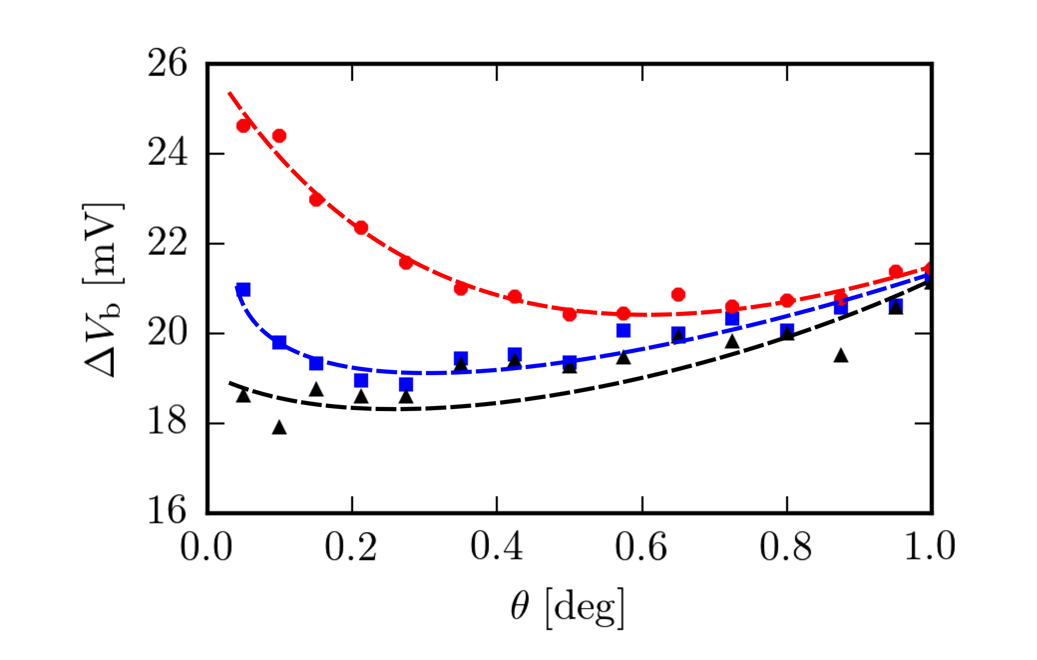
Peaks in the current density at collinearity are symmetric with respect to for , as in Fig. 3, while the current profile is asymmetric for finite values of , as in Fig. 5. The asymmetry between the two graphene layers is a consequence of the position of the gate layer. The value of the inter-layer bias potential at which the collinearity condition is met is found as explained in Fig. 2(b). Here, the dotted horizontal lines, displaying , are intersected with the solid line, displaying . For large regions of parameter space, the peak corresponding to () appears at negative (positive) bias voltages. However, at very small angles and sufficiently large , the collinearity condition with both may be met at .
The tunneling current density at finite temperature and for vanishing gate voltage is shown in Fig. 3. Data in this figure have been obtained by using Eq. (16) for the quasiparticle lifetime. Peaks at collinearity are evident and located at bias voltages close to those predicted on the basis of the simple expression (18). Increasing temperature, the peaks become broader and drift to slightly larger absolute values of the bias potential. Moreover, the linear dependence of the current on the bias voltage around becomes steeper as temperature increases. Comparing the current profiles for two different values of the misalignment angle in the two panels of Fig. 3, we see that these effects are much more evident for small misalignment angles. This behavior is due to the fact that, for large values of , broadening of the current peak is dominated by lattice misalignment effects, while e-e interactions play the most important role in the condition of near-alignment. Indeed, temperature affects the tunneling current through the suppression of the quasiparticle lifetime , i.e. broadening of the spectral function. A broader spectral function entails a more relaxed energy conservation in the tunneling processes, and thus the collinear peak widens around its zero-temperature, geometrically-deduced position. Varying temperature has no effect on the current profile, if the quasiparticle lifetime is not affected by e-e interactions. Our results thus show that the tunneling current at sufficiently small misalignment angles bear clear signatures of e-e interactions. This is central result of this Article.
To quantify the role of e-e interactions, in Fig. 4 we plot the broadening of the current peak as a function of the misalignment angle for various temperatures. Since the current profile around the peak is not symmetric and extends to large values of the bias voltage , the definition of “peak broadening” is not obvious. Therefore, we adopt an ad hoc definition to estimate how temperature affects the peak broadening. We define the broadening as the standard deviation , where the average
| (19) |
is defined with respect to the current profile. The extremes of integration , are symmetric around the peak position with a total extent . Fig. 4 shows that the broadening of the current peak depends on temperature—a clear signature of e-e interactions. However, the temperature dependence is weak at misalignment angles (where the tunneling current away from collinearity is suppressed by lattice misalignment) and stronger at (where the effect of e-e interactions becomes more important).
At low temperatures, a further signature of the electron spectral properties is found by studying the profile of the tunneling current as a function of gate voltage. This is shown in Fig. 5. Data in this figure have been obtained by using Eq. (17) for the quasiparticle lifetime. We have decided not to calculate the value of the current for ranges of such that bottom- or top-layer carrier densities are smaller than . This is because the normal Fermi liquid expression (17) for the quasiparticle decay rate is not justified near the charge neutrality point. In these regions, the derivative of the carrier density of either layer with respect to vanishes (see Fig. 2). As a consequence, the differential conductance is nearly zero, as observed experimentally mishchenko_naturenano_2014 ; britnell_naturecommun_2013 .
We observe that for small misalignment angles and large gate voltages the peak corresponding to the collinearity condition with [indicated by arrows in Fig. 5(a)] is located at . In this regime, the height of the peak is very sensitive to disorder and increases as the residual spectral width decreases. This is because the most important contribution to the energy integral in Eq. (4)—due to collinearity—arises from a region in the plane where is small [see inset in Fig. 5(a)]. That is, the dominant contribution to the tunneling current comes from particles tunneling from the neighborhood of the chemical potential in one cone to the neighborhood of the chemical potential in the other cone. In this case, the e-e contribution to the quasiparticle lifetime tends to zero, as in all Fermi liquids, so that both the initial and final states involved in the tunneling process are long-lived and the tunneling probability is enhanced. The finite height of the current peak is determined by the the residual spectral width due to disorder. Similarly to the effect of e-e interactions at finite temperature, the effect of the residual spectral width is suppressed at larger misalignment angles [see Fig. 5(b)], where the width and height of the current peaks is rather insensitive to the value of gate voltage.
V Summary
In this Article we have presented a theory of the tunneling characteristics between misaligned graphene layers, which takes into account the spectral properties of the tunneling electrons. We have taken into account quasiparticle lifetime effects into the quasiparticle spectral function by treating on an equal footing electron-electron interactions and elastic scattering off of the static disorder potential. Effects of electron-electron interactions on the quasiparticle lifetime are considered separately at finite (Figs. 3-4) and very low (Fig. 5) temperatures. In both cases, we study the interplay between the misalignment angle and the quasiparticle lifetime.
The profile of the tunneling current as a function of the bias voltage is characterized by peaks which originate from the enhanced tunneling probability between electronic states with collinear wave vectors in the two layers. Due to electron-electron interactions, the broadening of these peaks depends on temperature at small misalignment angles. In this regime, comparing experimental data with our theoretical results enables measurements of the quasiparticle lifetime in a vertical transport experiment. At very low temperatures, instead, by tuning the gate voltage, it is possible to reach a regime in which the height of one current peak is entirely determined by the quasiparticle lifetime due to elastic scattering. Both effects disappear when the misalignment angle is larger than -, because, in this case, the width of the current peaks is dominated by the non-conservation of in-plane wave vector during the tunneling process.
Measurements of can be compared with many-body theory calculations polini_arxiv_2014 ; li_prb_2013 ; principi_arxiv_2015 and are important to assess the region of parameter space (carrier density and temperature) where transport in massless Dirac fermion fluids can be described by hydrodynamic theory bandurin_arxiv_2015 ; torre_prb_2015 .
Acknowledgements.
K.A.G.B. acknowledges useful discussions with J.R. Wallbank, P. D’Amico, and G. Borghi. This work was supported by the EC under the Graphene Flagship program (contract no. CNECT-ICT-604391) and MIUR through the program “Progetti Premiali 2012” - Project “ABNANOTECH”. We have made use of free software python .References
- (1) G.D. Mahan, Many Particle Physics (Plenum, New York, 1981).
- (2) P. Noziéres, Theory of Interacting Fermi Systems (W.A. Benjamin, Inc., New York, 1964).
- (3) D. Pines and P. Noziéres, The Theory of Quantum Liquids (W.A. Benjamin, Inc., New York, 1966).
- (4) G.F. Giuliani and G. Vignale, Quantum Theory of the Electron Liquid (Cambridge University Press, Cambridge, 2005).
- (5) B.L. Altshuler, A.G. Aronov, and D.E. Khmelnitsky, J. Phys. C 15, 7367 (1982).
- (6) J. Imry and A. Stern, Semicond. Sci. Technol. 9, 1879 (1994).
- (7) A. Damascelli, Z. Hussain, and Z.-X. Shen, Rev. Mod. Phys. 75, 473 (2003).
- (8) A. Bostwick, T. Ohta, T. Seyller, K. Horn, and E. Rotenberg, Nature Phys. 3, 36 (2007).
- (9) S.Y. Zhou, G.-H. Gweon, A.V. Fedorov, P.N. First, W.A. der Heer, D.-H. Lee, F. Guinea, A.H. Castro Neto, and A. Lanzara, Nature Mater. 6, 770 (2007).
- (10) A. Bostwick, F. Speck, T. Seyller, K. Horn, M. Polini, R. Asgari, A.H. MacDonald, and E. Rotenberg, Science 328, 999 (2010).
- (11) A.L. Walter, A. Bostwick, K.-J. Jeon, F. Speck, M. Ostler, T. Seyller, L. Moreschini, Y.J. Chang, M. Polini, R. Asgari, A.H. MacDonald, K. Horn, and E. Rotenberg, Phys. Rev. B 84, 085410 (2011).
- (12) D.A. Siegel, C.-H. Park, C. Hwang, J. Deslippe, A.V. Fedorov, S.G. Louie, and A. Lanzara, Proc. Natl. Acad. Sci. (USA) 108, 11365 (2011).
- (13) S.Q. Murphy, J.P. Eisenstein, L.N. Pfeiffer, and K.W. West, Phys. Rev. B 52, 14825 (1995).
- (14) A.V. Chaplik, Sov. Phys. JETP 33, 997 (1971).
- (15) C. Hodges, H. Smith, and J.W. Wilkins, Phys. Rev. B 4, 302 (1971).
- (16) G.F. Giuliani and J.J. Quinn, Phys. Rev. B 26, 4421 (1982).
- (17) H. Fukuyama and E. Abrahams, Phys. Rev. B 27, 5976 (1983).
- (18) T. Jungwirth and A.H. MacDonald, Phys. Rev. B 53, 7403 (1996).
- (19) L. Zheng and S. Das Sarma, Phys. Rev. B 53 9964 (1996).
- (20) M. Reizer and J.W. Wilkins, Phys. Rev. B 55, R7363 (1997).
- (21) D.C. Marinescu, J.J. Quinn, and G.F. Giuliani, Phys. Rev. B 65 045325 (2002)
- (22) Z. Qian and G. Vignale, Phys. Rev. B 71, 075112 (2005).
- (23) A.K. Geim and I.V. Grigorieva, Nature 499, 419 (2013).
- (24) L. Britnell, R.V. Gorbachev, R. Jalil, B.D. Belle, F. Schedin, M.I. Katsnelson, L. Eaves, S.V. Morozov, A.S. Mayorov, N.M.R. Peres, A.H. Castro Neto, J. Leist, A.K. Geim, L.A. Ponomarenko, and K.S. Novoselov, Nano Lett. 12, 1707 (2012).
- (25) L. Britnell, R.V. Gorbachev, R. Jalil, B.D. Belle, F. Schedin, A. Mishchenko, T. Georgiou, M.I. Katsnelson, L. Eaves, S.V. Morozov, N.M.R. Peres, J. Leist, A.K. Geim, K.S. Novoselov, and L.A. Ponomarenko, Science 335, 949 (2012).
- (26) L. Britnell, R.V. Gorbachev, A.K. Geim, L.A. Ponomarenko, A. Mishchenko, M.T. Greenway, T.M. Fromhold, K.S. Novoselov, and L. Eaves, Nature Commun. 4, 1794 (2013).
- (27) A. Mishchenko, J.S. Tu, Y. Cao, R.V. Gorbachev, J.R. Wallbank, M.T. Greenaway, V.E. Morozov, S.V. Morozov, M.J. Zhu, S.L. Wong, F. Withers, C.R. Woods, Y-J. Kim, K. Watanabe, T. Taniguchi, E.E. Vdovin, O. Makarovsky, T.M. Fromhold, V.I. Fal’ko, A.K. Geim, L. Eaves, and K.S. Novoselov, Nature Nanotech. 9, 808 (2014).
- (28) B. Fallahazad, L. Kayoung, K. Sangwoo Kang, J. Xue, S. Larentis†, C. Corbet†, K. Kim, H.C.P. Movva, T. Taniguchi, K. Watanabe, L.F. Register, S.K. Banerjee, and E. Tutuc, Nano Lett. 15, 1 (2015).
- (29) R.M. Feenstra, D. Jena, and G. Gu, J. Appl. Phys. 111 043711 (2012).
- (30) S.C. de la Barrera, Q. Gao, and R.M. Feenstra, J. Vac. Sci. Technol. B 32, 04E101 (2014).
- (31) L. Brey, Phys. Rev. App. 2, 014003 (2014).
- (32) J.R. Wallbank, Electronic Properties of Graphene Heterostructures with Hexagonal Crystals (Springer PhD Thesis Series, Springer, 2014).
- (33) T.L.M. Lane, J.R. Wallbank, and V.I. Fal’ko, Appl. Phys. Lett. 107, 203506 (2015).
- (34) V.N. Kotov, B. Uchoa, V.M. Pereira, F. Guinea, and A.H. Castro Neto, Rev. Mod. Phys. 84, 1067 (2012).
- (35) R. Bistritzer and A.H. MacDonald, Phys. Rev. B 81, 245412 (2010).
- (36) R. Bistritzer and A.H. MacDonald, Proc. Nat. Acad. Sci. USA 108, 12233 (2011).
- (37) R. Bistritzer and A.H. MacDonald, Phys. Rev. B 84, 035440 (2011).
- (38) E.J. Mele, Phys. Rev. B 84, 235439 (2011).
- (39) J.M.B. Lopes dos Santos, N.M.R. Peres, and A.H. Castro Neto, Phys. Rev. B 86, 155449 (2012).
- (40) R.V. Gorbachev, A.K. Geim, M.I. Katsnelson, K.S. Novoselov, T. Tudorovskiy, I.V. Grigorieva, A.H. MacDonald, S.V. Morozov, K. Watanabe, T. Taniguchi, and L.A. Ponomarenko, Nature Phys. 8, 896 (2012).
- (41) M. Carrega, T. Tudorovskiy, A. Principi, M.I. Katsnelson, and M. Polini, New J. Phys. 14, 063033 (2012).
- (42) E.L. Wolf, Principles of Electron Tunneling Spectroscopy (Oxford University Press, New York, 2012).
- (43) M. Polini, R. Asgari, G. Borghi, Y. Barlas, T. Pereg-Barnea, and A.H. MacDonald, Phys. Rev. B 77, 081411(R) (2008).
- (44) A. Tomadin, A. Principi, J.C.W. Song, L.S. Levitov, and M. Polini, Phys. Rev. Lett. 115, 087401 (2015).
- (45) Y. Barlas, T. Pereg-Barnea, M. Polini, R. Asgari, and A.H. MacDonald, Phys. Rev. Lett. 98, 236601 (2007).
- (46) R. Asgari, M.I. Katsnelson, and M. Polini, Ann. Phys. (Berlin) 526, 359 (2014).
- (47) E.H. Hwang and S. Das Sarma, Phys. Rev. B 77, 081412(R) (2008).
- (48) M. Polini and G. Vignale, The quasiparticle lifetime in a doped graphene sheet. In No-nonsense physicist: an overview of Gabriele Giuliani’s work and life (eds. M. Polini, G. Vignale, V. Pellegrini, and J.K. Jain) (Edizioni della Normale, Pisa, 2015). Also available as arXiv:1404.5728 (2014).
- (49) Q. Li and S. Das Sarma, Phys. Rev. B 87, 085406 (2013).
- (50) A. Principi, M. Polini, R. Asgari, and A.H. MacDonald, Solid State Commun. 152, 1456 (2012).
- (51) D. Brida, A. Tomadin, C. Manzoni, Y. J. Kim, A. Lombardo, S. Milana, R.R. Nair, K.S. Novoselov, A.C. Ferrari, G. Cerullo, and M. Polini, Nature Commun. 4, 1987 (2013).
- (52) A. Tomadin, D. Brida, G. Cerullo, A.C. Ferrari, and M. Polini, Phys. Rev. B 88, 035430 (2013).
- (53) A. Principi, G. Vignale, M. Carrega, and M. Polini, arXiv:1506.06030 (2015).
- (54) D.A. Bandurin, I. Torre, R. Krishna Kumar, M. Ben Shalom, A. Tomadin, A. Principi, G.H. Auton, E. Khestanova, K.S. Novoselov, I.V. Grigorieva, L.A. Ponomarenko, A.K. Geim, and M. Polini, arXiv:1509.04165 (2015).
- (55) I. Torre, A. Tomadin, A.K. Geim, and M. Polini, Phys. Rev. B 92, 165433 (2015).
- (56) www.gnu.org, www.python.org.