High Responsivity, Large-Area Graphene/MoS2 Flexible Photodetectors
Abstract
We present flexible photodetectors (PDs) for visible wavelengths fabricated by stacking centimetre-scale chemical vapor deposited (CVD) single layer graphene (SLG) and single layer CVD MoS2, both wet transferred onto a flexible polyethylene terephthalate substrate. The operation mechanism relies on injection of photoexcited electrons from MoS2 to the SLG channel. The external responsivity is 45.5A/W and the internal 570A/W at 642nm. This is at least two orders of magnitude higher than bulk-semiconductor flexible membranes and other flexible PDs based on graphene and layered materials. The photoconductive gain is up to . The photocurrent is in the 0.1-100A range. The devices are semi-transparent, with just 8 absorption at 642nm and work stably upon bending to a curvature of 6cm. These capabilities and the low voltage operation ( 1V) make them attractive for wearable applications.
I Introduction
Modern electronic and opto-electronic systems such as smart phones, smart glasses, smart watches, wearable devices and electronic tattoos increasingly require ultra-thin, transparent, low-cost and energy efficient devices on flexible substratesAkinNC2014 . The rising demand for flexible electronics and optoelectronics requires materials which can provide a variety of electrical and optical functionalities, with constant performance upon application of strainRyha2010 . A wide range of optoelectronic devices on flexible substrates have been reported to date, such as photodetectors (PDs)YuanAPL2009 ; LiuOE2013 , light emitting diodes (LEDs)ParkS2009 , optical filtersQianAPL2008 , optical interconnectsChenNM2011 ; BosmPTL2010 , photovoltaic devicesShahNP2010 ; YoonNC2011 and biomedical sensorsKoN2008 ; KimS2011 .
Major challenges in the development of flexible optoelectronic devices stem from the limitations associated with the high stiffness of bulk semiconductorsMacmJMS1972 ; BlakJAP1982 . In the case of flexible PDs, the current approaches primarily rely on thin (m-thick) semiconductor membranesYangAPL2010 ; YuanAPL2009 and compound semiconductor nanowires (NWs)LeeMEMS2012 ; LiuOE2013 ; ChenJMCC2014 ; YuJMCC2014 , mainly because of their ability to absorb light throughout the whole visible range (0.4-0.7m) and the possibility to adapt their fabrication techniques from rigid to plastic, or deformable substratesAkinNC2014 .
One of the key parameters for PDs characterization is the responsivity. This is defined as the ratio between the collected photocurrent () and the optical power. The responsivity is named external ()Sze2006 or internal ()Sze2006 , whenever the incident () or absorbed () optical power is used at the denominator. Since not all incident photons are absorbed, i.e. , then is typically larger than Sze2006 .
In flexible PDs, up to was reported for crystalline semiconductor membranes (InP, Ge)YangAPL2010 ; YuanAPL2009 with integrated p-i-n junctions, showing photocurrent up to, with degradation upon bending at a radius 3cmYangAPL2010 . PDs made of a single semiconductor NW on flexible substratesLeeMEMS2012 ; LiuOE2013 ; ChenJMCC2014 ; YuJMCC2014 demonstrated up to, for down to 0.3cmLiuOE2013 . Yet, these provide limited in the order of LiuOE2013 ; ChenJMCC2014 ; YuJMCC2014 up to less than LeeMEMS2012 . For flexible devices exploiting NW-arrays by drop-castingLiuOE2013 ; ChenJMCC2014 ; YuJMCC2014 , rather than based on single-NWs, degrades significantly from to the rangeLiuOE2013 ; ChenJMCC2014 ; YuJMCC2014 , due to photocurrent loss at multiple junctions in the NW networkLiuOE2013 ; ChenJMCC2014 ; YuJMCC2014 .
Graphene and related materials (GRMs) have great potential in photonics and optoelectronicsBonaNP2010 ; FerrN2015 ; SunACS2010 ; KoppNN2014 . A variety of GRM-based devices have been reported, such as flexible displaysKimN2009 , photovoltaic modulesBaugNN2014 ; PospNN2014 , photodetectorsKoppNN2014 ; XiaNN2009 ; KisNN2013 , optical modulatorsLiuN2011 , plasmonic devicesChenN2012 ; FeiN2012 ; JuNN2011 ; YanNN2012 ; EchtNC2011 , and ultra-fast lasersSunACS2010 . Heterostructures, obtained by stacking layers of different materials were also exploredFerrN2015 ; KoppNN2014 , e.g. in photovoltaicFurcNL2014 and light emitting devicesWithNM2015 . Refs.37; 38 reported SLG/MoS2-based PDs made of mechanically exfoliatedRoyNN2013 or CVD grownZhanSR2014 materials, transferred on Si/SiO2 rigid substrates. These reached back-gate dependent 108A/W for optical intensities0.1pW/m2.
GRM based flexible PDs have been reported for visible light (WithNL2014 ; FinnJMCC2014 ) using materials produced by liquid phase exfoliation (LPE)HernNN2008 ; BonaMT2012 of graphene and transition metal dichalcogenides (TMDs)WithNL2014 ; FinnJMCC2014 . In Ref.40, a flexible PD on polyethylene terephthalate (PET) was fabricated by sandwiching a LPE dispersion of WS2 between a LPE graphene film serving as a back electrode and a chemical vapor deposited (CVD) graphene top electrode, with 0.1mA/W. This value is orders of magnitude lower compared to other flexible PDsYangAPL2010 ; YuanAPL2009 ; LeeMEMS2012 ; LiuOE2013 ; ChenJMCC2014 ; YuJMCC2014 . The lower in LPE-based devices is attributed to non-efficient inter-flake charge transferKingACS2010 ; TorrNN2014 , resulting in limited conductivityKingACS2010 ; TorrNN2014 and poor collection of photo-generated carriers at the outer metal electrodesWithNL2014 . Similarly, the inefficient charge transfer affected (in the range) in Ref.39, where a PD was fabricated with LPE MoS2 as absorber and LPE graphene as top electrode.
Here we take advantage of the mechanical properties of layered materials to demonstrate flexible gate-controlled SLG/MoS2 PDs for visible wavelengths with of tens of A/W and optical transparency. The devices are assembled by stacking on a PET substrate a centimetre-scale CVD SLG on a CVD-grown single layer MoS2 (1L-MoS2). In this configuration, 1L-MoS2 acts as visible light absorber, while SLG is the conductive channel for flowZhanSR2014 ; RoyNN2013 . We show that increases either by promoting carrier injection from 1L-MoS2 to SLG using polymer electrolyte gating, or by increasing the source-drain voltage. We get up to applying a 1V bias with tens . These values are at least two orders of magnitude higher than those reported in semiconductor membranes devicesYangAPL2010 ; YuanAPL2009 , semiconductor NW arraysLeeMEMS2012 ; LiuOE2013 ; ChenJMCC2014 ; YuJMCC2014 and GRM-basedWithNL2014 ; FinnJMCC2014 flexible PDs operating in the visible rangeYangAPL2010 ; YuanAPL2009 ; LeeMEMS2012 ; LiuOE2013 ; ChenJMCC2014 ; YuJMCC2014 ; WithNL2014 ; FinnJMCC2014 . This is achieved in devices with transparency, twice that reported for semiconductor membrane devicesYangAPL2010 . We get A/W for0.1nW/m2 at 642nm, similar to SLG/MoS2 PDsZhanSR2014 ; RoyNN2013 on rigid substrate operating at the same optical power level. This shows that SLG/MoS2 heterostructures on PET retain their photodetection capabilities. Upon bending, our devices have stable performance for rb down tocm. This is comparable to rb measured in semiconductor membranes PDsYangAPL2010 ; YuanAPL2009 , which show lower () responsivitiesYangAPL2010 ; YuanAPL2009 . Although our rb is one order of magnitude larger than for flexible single NWsLeeMEMS2012 ; LiuOE2013 ; ChenJMCC2014 ; YuJMCC2014 , the latter had at least three orders of magnitude smaller device areas ()LeeMEMS2012 ; LiuOE2013 ; ChenJMCC2014 ; YuJMCC2014 compared to our PDs (). Given the responsivity, flexibility, transparency and low operation voltage (below ), our PDs may be integrated in wearable, biomedical and low-power opto-electronic applicationsLeeMEMS2012 ; KoN2008 ; KimS2011 .
II Results and discussion

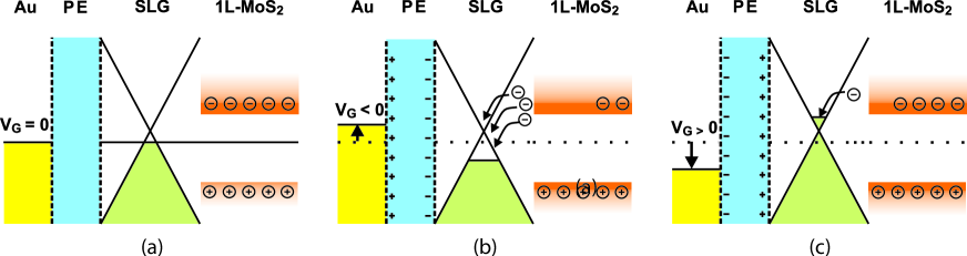
Fig.1 plots a schematic drawing of our PD. The device consists of a 1L-MoS2 absorber covered by a SLG channel, clamped between source and drain electrodes. We chose PET as a flexible substrate due to its90% transparency in the visible rangeFaraOAM2011 and ability to withstand solventsMartPNAS2013 (e.g acetone and isopropyl alcohol) commonly used in the transfer processes of 2d materials grown by CVD (e.g. transfer of SLG grown on Cu)BaeNN2010 . The SLG/1L-MoS2 heterostructure is gated using a polymer electrolyteDasPRB2009 ; DasNN2008 .
The operation principle of our devices is depicted in Fig.2. For energy bands alignment, the electron affinity of 1L-MoS2 and the Dirac point of SLG are assumed to be4-4.2eVChoiNC2013 ; DasNL2013 and4.6eVYuNL2009 ; ShanPRL2005 , respectively. We also assume SLG to be initially p-doped (Fig.2a), as reported in previous works involving SLG transferred on PET substratesKimNL2010 ; LeeNL2012 . In thermodynamic equilibrium, is constant across the device and is located below the Dirac point. During illumination, part of the photo-generated electrons would be injected from the 1L-MoS2 conduction band into the p-doped SLGZhanSR2014 ; RoyNN2013 , leaving behind uncompensated photogenerated holes. The latter would act as an additional positive to the SLG channel, seen as a shift of the charge neutrality point () to more negative voltages. In p-doped SLG, the injected electrons from 1L-MoS2 would occupy energy states above (Fig.2b), thus reducing the concentration of holes and decreasing the PD current. Electron injection can be further promoted by gating. When negative is applied, higher p-doping of the SLG channel would induce a stronger electric field at the SLG/1L-MoS2 interfaceZhanSR2014 , thus favoring electron transfer from 1L-MoS2 (Fig.2b). Hence, for negative , is expected to increase, due to injection of more electrons and consequent more pronounced PD current reduction. The opposite should happen for positive , where the gate-induced negative charge in SLG would reduce the p-doping and shift towards the Dirac point. In this case, the photogenerated electrons in 1L-MoS2 would experience weaker electric fields, becoming less attracted by the SLG channel. As a result, we expect to decrease. When positive is high enough, would cross the Dirac point and SLG would become n-doped (Fig.2c). Thus, only weak electron injection from 1L-MoS2 would be possible if in SLG remains below the 1L-MoS2 conduction band; the transferred electrons increase free-carriers concentration in the n-doped channel, hence minor increments of and are expected.
Our devices are built as follows. 1L-MoS2 is epitaxially grown by CVD on c-plane sapphire substratesDumcACS2015 . These are annealed at 1000∘C in air for 1 hour after consecutive cleaning by acetone/isopropyl alcohol/deionized (DI) water. They are then placed face-down above a crucible containing5mg MoO3 (99.998% Alfa Aesar). This is loaded into a 32mm outer diameter quartz tube placed in a split-tube three-zone furnace. A second crucible containing 350mg sulfur ( 99.99% purity, Sigma Aldrich) is located upstream from the growth substrates. Ultrahigh-purity Ar is used as carrier gas at atmospheric pressure. The procedure is: ramp the temperature to 300∘C with 200sccm Ar flow, set to 300∘C for 10mins, ramp to 700∘C (50∘C/min increase temperature rate) with 10sccm Ar flow, set at 700∘C for 10 min, cool to 570∘C with 10sccm of Ar, increase the gas flow to 200sccm and open the furnace for rapid coolingDumcACS2015 . SLG is grown on 35m Cu foil, following the process described in Ref.47. The substrate is annealed in hydrogen atmosphere (H2, 20sccm) up to C for 30 minutes. Then, 5sccm CH4 is added to initiate growthLiS2009 ; BaeNN2010 . The sample is then cooled in vacuum (1mTorr) to room temperature and removed from the chamber.
Prior to assembling the SLG/MoS2 stack, the quality and uniformity of MoS2 on sapphire and SLG on Cu are inspected by Raman spectroscopy and photoluminescence (PL), using a Horiba Jobin Yvon HR800 spectrometer equipped with a 100X objective. The laser power is kept below 100W (spot size m in diameter) to avoid possible heating effects or damage. Fig.3a (green curve) plots the Raman spectrum of CVD MoS2 on sapphire for 514nm excitation. The peak atcm-1 corresponds to the in-plane (E) modeVerbPRL1970 ; WietPRB1971 , while that at404cm-1, is the out of plane (A1g) modeVerbPRL1970 ; WietPRB1971 , with full width at half maximum FWHM(E)=2.5 and FWHM(A1g)=3.6cm-1, respectively. The E mode softens, whereas the A1g stiffens with increasing layer thicknessLeeACS2010 ; LiAFM2012 , so that their frequency difference can be used to monitor the number of layersLeeACS2010 . The peak position difference20cm-1 is an indicator of 1L-MoS2LeeACS2010 . The peak atcm-1 (marked by asterisk in Fig.3a) corresponds to the A1g mode of sapphirePortJCP1967 .
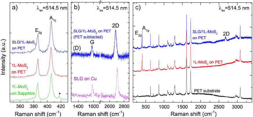
The Raman spectrum measured at 514 nm of SLG on Cu is shown in Fig.3b (magenta curve). This is obtained after the removal of the non-flat background PL of CuLagaAPL2013 . The two most intense features are the G and the 2D peak, with no significant D peak. The G peak corresponds to the E2g phonon at the Brillouin zone centreFerrNN2013 . The D peak is due to the breathing modes of sp2 rings and requires a defect for its activation by double resonanceFerrPRL2006 ; CancNL2011 ; FerrNN2013 ; FerrPRB2000 . The 2D peak is the second order of the D peakFerrNN2013 . This is always seen, even when no D peak is present, since no defects are required for the activation of two phonons with the same momentum, one backscattering from the otherFerrNN2013 . In our sample, the 2D peak is a single sharp Lorentzian with FWHM(2D)26cm-1, a signature of SLGFerrPRL2006 . Different (20) measurements show similar spectra, indicating uniform quality. The position of the G peak, Pos(G), is1589cm-1, with FWHM(G)13cm-1. The 2D peak position, Pos(2D) is2698cm-1, while the 2D to G peak intensity and area ratios, I(2D)/I(G) and A(2D)/A(G), are 2.6 and 5.8, respectively, indicating a p-doping300meVDasNN2008 ; BrunACS2014 ; BaskPRB2009 , which corresponds to a carrier concentration51012cm-2.
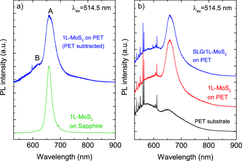
Another evidence for 1L-MoS2 comes from the PL spectrum [Fig.4a (green curve)], showing a peak658nm (1.88eV), due to band-to-band radiative recombination of electron-hole pairs in 1L-MoS2MakPRL2010 .
Then, the MoS2 film is transferred onto a PET substrate from sapphire using a KOH-based approachDumcACS2015 . The samples are first spin coated with100nm polymethyl methacrylate (PMMA). This is detached in a 30% KOH solution, washed in DI water and transferred onto PET. The PMMA is then dissolved in acetone. Subsequently, SLG is transferred on the 1L-MoS2 on PET. PMMA is spin coated on the SLG/Cu substrate, then placed in a solution of ammonium persulfate (APS) in DI water until Cu is etchedBaeNN2010 ; BonaMT2012 . The PMMA membrane with attached SLG is then transferred to a beaker filled with DI water for cleaning APS residuals. The membrane is subsequently lifted with the target PET substrate having 1L-MoS2 on top. After drying, PMMA is removed in acetone leaving SLG on 1L-MoS2.
Raman and PL characterizations are performed at each step of the SLG/1L-MoS2 assembly on PET, i.e on 1L-MoS2 transferred on PET, and on SLG on 1L-MoS2. This is to confirm no degradation during the fabrication process. For 1L-MoS2 on PET, the Raman at 514nm is shown, with a close-up of the E and A1g regions, in Fig.3a (red curve). The frequency difference between E and A1g and the FWHMs are preserved on PET, suggesting no degradation. The PL spectrum of 1L-MoS2 on PET is shown in Fig.4b (red curve). The signal from 1L-MoS2 is convolved within the background due to the PET substrate [Fig.4b (black curve)]. In order to reveal the underlying PL signature of 1L-MoS2, we use a point-to-point subtraction between the spectrum of 1L-MoS2 on PET [Fig.4b (red curve)] and the reference PET spectrum [Fig.4b (black curve)]. Prior to subtraction, the spectra are normalized to the intensity of the Raman peak at1615cm-1 (corresponding to the peak at560nm in Fig.4b), due to the stretching vibrations of benzene rings in PETBoerJPS1976 . As a result, the PL signal of 1L-MoS2 can be seen in Fig.4a (blue curve) revealing no significant changes after transfer. The subsequent transfer of SLG on 1L-MoS2 does not alter the 1L-MoS2 PL position and lineshape [Fig.4b (blue curve)].
We then characterize the SLG transferred on 1L-MoS2/PET. The intense Raman features of the underlying PET substrateBoerJPS1976 [Fig.3c (black curve)], mask the SLG peaks. In order to reveal the Raman signatures of SLG, we first measure the reference spectrum, shown in Fig.3c (black curve), of a PET substrate, using identical experimental conditions as those for SLG/1L-MoS2/PET. We then implement a point-to-point subtraction, normalized to the intensity of the PET peak at 1615cm-1, of the PET reference spectrum from the total spectrum Fig.3c (blue curve). The result is in Fig.3b (blue curve). The 2D peak retains its single-Lorentzian line-shape with FWHM(2D)28cm-1, validating the SLG transfer. The negligible D peak indicates that no significant defects are induced during transfer. Pos(G) is1584cm-1, FWHM(G)15cm-1, Pos(2D)2685cm-1, I(2D)/I(G)2.9 and A(2D)/A(G)5.9, indicating a p-doping31012cm-2 (200meV)DasNN2008 ; BaskPRB2009 .
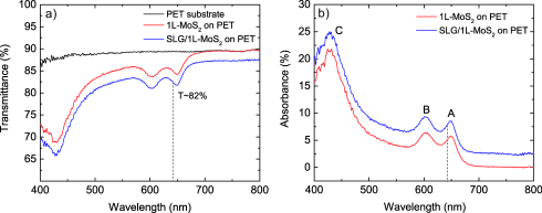
We then measure the absorption and transmission of SLG/1L-MoS2 using a broadband (400-1300nm) white light from a tungsten halogen lamp. The transmitted light is collected by a 10x objective lens (NA=0.25) with a Horiba Jobin Yvon HR800 spectrometer equipped with a 300 grooves/mm grating, charged coupled device (CCD) detector and a m pinhole. Fig.5a plots the optical transmittance of bare PET (, black line), 1L-MoS2 on PET (, red line) and the final SLG/1L-MoS2 stack on PET (, blue line) measured in the 400-800nm wavelength range. Fig.5b plots the absorption of 1L-MoS2 on PET (, red line) and of SLG/1L-MoS2 on PET (, blue line), calculated as =(-)/ and =(-)/. The three peaks in Fig.5b at 650nm (1.91eV), 603nm (2.06eV), and 428nm (2.90eV) correspond to the A, B, C excitons of 1L-MoS2QiuPRL2013 ; MakPRL2010 . The positions of the A, B and C peaks remain unchanged after SLG transfer. The difference between the two curves (red and blue) is 2.6%, consistent with the additional SLG absorptionNairS2008 .
The PD area is shaped by etching, whereby SLG extending beyond the 1L-MoS2 layer is removed in an oxygen plasma. The source-drain and gate electrodes are then defined by patterning the contacts area, followed by Cr/Au (6nm/60nm) evaporation and lift-off. PDs with different channels lengths (100m-1mm), 2mm channel width and common side-gate electrodes (1cm x 0.5cm) are built, Fig.1b.
Refs.37,38 showed that the responsivity of SLG/MoS2 PDs can be enhanced by gating. This induces a stronger electric field at the SLG/MoS2 interface and promotes charge transfer. Various gating techniques have been exploited for GRM-based devices, including conventional Si/SiO2 back-gatesNovoN2005 , high-k dielectrics (Al2O3, HfO2)LemmEDL2007 , chemical dopantsWehlACS2008 , ionic liquidsYePNAS2011 and polymer electrolytes (PE)DasNN2008 ; BrunACS2014 . In order to gate our SLG/1L-MoS2 on PET, we employ the latter due to its compatibility with flexible substratesSirrS2000 and the ability to substantially dope SLG ()DasNN2008 ; BrunACS2014 using small gate voltages (up to 4V), unlike other gating techniques, which would require considerably higher biases to reach the same dopingNovoN2005 ; WehlACS2008 . We use a PE consisting of LiClO4 and polyethylene oxide (POE)DasNN2008 ; BrunACS2014 . We place the PE over both the SLG channel and the side-gate electrode, and use in order to avoid electrochemical reactions, such as hydrolysis of residual water in the electrolyteAzaiJPS2007 ; EfetPRL2010 . These reactions may permanently modify the SLG electrodeAzaiJPS2007 ; EfetPRL2010 , and compromise the stability and performance of the device.
We characterize the responsivity at 642nm (1.93eV), slightly above the A exciton peak, where absorption of 1L-MoS2 is maximized (Fig.5b). At 642nm the SLG/1L-MoS2 heterostructure shows8% absorption (Fig.5b) and the device retains82% transparency (Fig.5a).
The measurements in Fig.6a are done at room temperature using a probe station and a parameter analyzer (Keithley 4200). The PD is illuminated at normal incidence by a collimated laser with ranging from 100W to 4mW. At these and with we measure a positive ranging from to , indicating an initial SLG p-doping220meV, consistent with the Raman estimate.
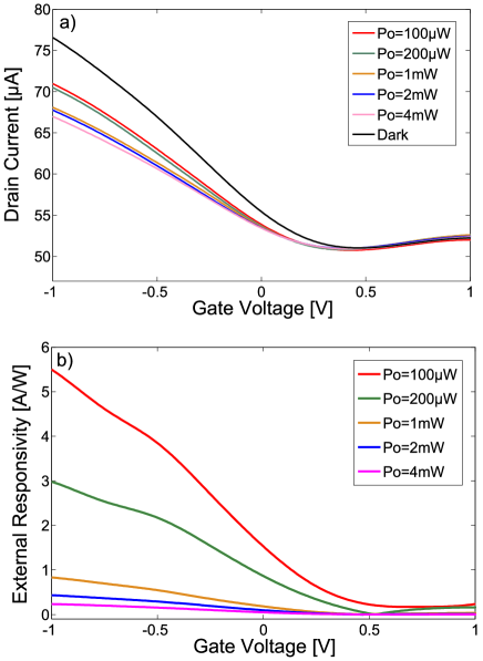
Fig.6a shows that, for where SLG transport is hole dominated, the current decreases under illumination ( at ), as anticipated from the band-diagram of Fig.2. For , where SLG is electron-doped, the PD shows a small (up to) current increase under illumination. Fig.6b plots as a function of , as derived from transconductance measurements usingSze2006 :
| (1) |
where and are the PD current under illumination and in dark, , is the laser spot area, is the PD area, and is a scaling factor that takes into account the fact that only a fraction of optical power impinges the PD. As expected from the band-diagram in Fig.2, tends to increase for more negative , up to at , for . By taking into account that only 8% of light is absorbed (, we derive . Fig.6b implies that the higher , the lower . This can be explained considering that the more photo-generated electrons are injected into the p-doped channel, the lower the electric field at the SLG/1L-MoS2 interface, therefore a reduced injection of electrons causes to decrease.
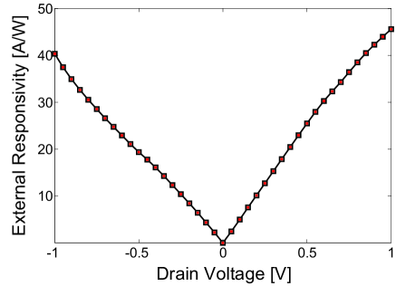
Given that , we expect a photoconductive gain ()Sze2006 ; KonstNN2012 , whereby absorption of one photon results in multiple charge carriers contributing to Iph. Our PDs act as optically-gated photoconductors, where the SLG conductance is modulated by optical absorption in the 1L-MoS2. In this configuration, the presence of implies that the injected electrons in SLG can recirculate multiple times between source and drain, before recombining with trapped holes in 1L-MoS2. Consequently, can be estimated as the ratio of electrons recombination () and transit () times in the SLG channel: FerrN2015 ; KoppNN2014 ; Sze2006 ; KonstNN2012 . For higher , the free carriers drift velocity in the SLG channel increases linearly with bias (Ohmic region) until it saturates, because of carriers scattering with optical phononsMeriNN2008 . The linear increase in results in shorter , i.e is defined as , where is the channel lengthFerrN2015 ; KoppNN2014 ; Sze2006 ; KonstNN2012 . Therefore, is also expected to grow linearly with , providing higher . To confirm the photoconductive nature of in our device and test the dependence of on , we measure under illumination at for and calculate using Eq.1. We use to keep the device operation in the linear (Ohmic) regime and minimize effect of non-linear dependence of on (such as velocity saturation) that might appear for MeriNN2008 . As shown in Fig.7, scales with and reaches () at . This is almost one order of magnitude higher than at , consistent with the similar increase in . These results are at least two orders of magnitude higher than semiconductor flexible membranesYangAPL2010 ; YuanAPL2009 and five orders of magnitude larger than other flexible PDs based on GRMsWithNL2014 ; FinnJMCC2014 .
We define as the ratio between electrons recirculating in the SLG channel, thus sustaining , and the initial electron concentration injected into SLG from 1L-MoS2ZhanSR2014 :
| (2) |
where is the electron charge and is the concentration per unit area of the injected electrons. is equal to the trapped-hole concentration in 1L-MoS2, which is related to charge neutrality point shift in the transfer characteristics. To calculate , we first write the potential balance in the metal-dielectric-SLG structure. When is applied, it creates a gate-to-channel potential drop (), and it induces a local electrostatic potential in graphene channel ()Sze2006 ; DasNN2008 :
| (3) |
where and are the charge concentration and the geometrical capacitance per unit area associated with the gate electrode respectively. , reflecting the charge neutrality of the gate capacitor, with the charge carrier concentration per unit area in the channel. Any variations change . As a result:
| (4) |
which leads to:
| (5) |
where is the SLG quantum capacitanceFangAPL2007 ; XiaNN2009-2 that characterizes the changes of the channel potential as a result of additional gating , and is the total capacitance .
To calculate we first need to find and . In PE gating, is associated with the EDL at the SLG/electrolyte interfaceDasNN2008 ; LuNL2004 ; OzelNL2005 ; XiaNN2009-2 . The EDL acts like a parallel-plate capacitor with an dielectric layer thickness of the order of , so that , where is the PE dielectric constant, and is the vacuum permittivity. In principle, for a monovalent electrolyte, can be explicitly calculatedRuss1989 if the electrolyte concentration is known. However, in the presence of a polymer matrix, the electrolyte ions can form complexes with polymer chainsSalomon1994 , therefore the precise ion concentration is difficult to measure. For PE gating, different EDL thicknesses in the range have been reportedDasPRB2009 ; DasNN2008 ; LuNL2004 ; OzelNL2005 . To estimate in our devices we take DasNN2008 and the dielectric constant of the PEO matrix to be Boyd1983 , as done in Ref.48. As a result, we obtain . This is the same order of magnitude as the SLG XiaNN2009-2 . Therefore the latter cannot be neglected in Eq.5. is given byXiaNN2009-2 :
| (6) |
where is the reduced Planck constant, is the Fermi velocity of charge carriers in grapheneNovoN2005 ; ZhanN2005 and is the intrinsic carrier concentration in SLG near the Dirac point induced by charge impurities, defects and local potential fluctuations in the SLG channelChenNP2008 ; AdamPNAS2007 ; VictorPRB2007 ; XiaNN2009-2 . Using Raman and transconductance we estimate . From Eq.6 we then get at . From Fig.6a, and extracting between the dark current and the transfer curves measured under illumination, and with Eq.5, we get ranging from for going from to . As a result, we obtain at for different as shown in Fig.8. As discussed previously, becomes larger for higher . Thus, we measure an increase of almost order of magnitude ( at ) for going from to .

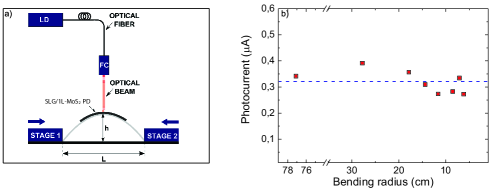
Finally, we test Iph as a function of bending. is estimated as , where is the chord of circumference connecting the two ends of the arc, and is the height at the chord midpoint. Fig.9b plots for different , showing a maximal deviation of for down to . This value is comparable to rb reported for semiconductor membrane PDsYangAPL2010 ; YuanAPL2009 , yet the latter show two orders of magnitude lower () responsivitiesYangAPL2010 ; YuanAPL2009 . Although our rb is one order of magnitude larger than reported by flexible single NW devicesLeeMEMS2012 ; LiuOE2013 ; ChenJMCC2014 ; YuJMCC2014 , the device area of our PDs () is at least four orders of magnitude larger compared to these devices ().
II.1 Conclusions
We reported flexible PDs for visible wavelengths with external responsivity up to45.5A/W and photoconductive gain of . This is at least two orders of magnitude higher than semiconductor flexible membranes and other GRM-based flexible PDs reported thus far. Our PDs show stable performance upon bending for radii of curvature larger than 6cm. The responsivity, flexibility, transparency and low operation voltage (below ) of our PDs makes them attractive candidates for wearable, biomedical and low-power opto-electronic applications.
We acknowledge funding from EU Graphene Flagship (no. 604391), ERC Grant Hetero2D, EPSRC Grants EP/K01711X/1, EP/K017144/1, EU grant GENIUS, a Royal Society Wolfson Research Merit Award
References
- (1) Akinwande, D., Petrone, N., Hone, J. Nat. Commun. 2014, 5.
- (2) Ryhaenen, T. T., 2010, Cambridge University Press.
- (3) Liu, Z., Chen, G., Liang, B., Yu, G., Huang, H., Chen, D., Shen, G. Opt. Express 2013, 21, 7799-7810.
- (4) Yuan, H.-C., Shin, J., Qin, G., Sun, L., Bhattacharya, P., Lagally, M. G., Celler, G. K., Ma, Z. Appl. Phys. Lett. 2009, 94, 13102.
- (5) Park, S.-I., Xiong, Y., Kim, R.-H., Elvikis, P., Meitl, M., Kim, D.-H., Wu, J., Yoon, J., Yu, C.-J., Liu, Z., et al. Science 2009, 325, 977-981.
- (6) Qiang, Z., Yang, H., Chen, L., Pang, H., Ma, Z., Zhou, W. App. Phys. Lett. 2008, 93, 061106.
- (7) Bosman, E., Van Steenberge, G., Van Hoe, B., Missinne, J., Vanfleteren, J., Van Daele, P. Photon. Technol. Lett., IEEE 2010, 22, 287-289.
- (8) Chen, Z., Ren, W., Gao, L., Liu, B., Pei, S., Cheng, H.-M. Nat. Mater. 2011, 10, 424-428.
- (9) Shahi, S. Nature Photon. 2010, 4, 506-506.
- (10) Yoon, J., Li, L., Semichaevsky, A. V., Ryu, J. H., Johnson, H. T., Nuzzo, R. G., Rogers, J. A. Nat. Commun. 2011, 2, 343.
- (11) Kim, D.-H., Lu, N., Ma, R., Kim, Y.-S., Kim, R.-H., Wang, S., Wu, J., Won, S. M., Tao, H., Islam, A., et al. Science 2011, 333, 838-843.
- (12) Ko, H. C., Stoykovich, M. P., Song, J., Malyarchuk, V., Choi, W. M., Yu, C.-J., Geddes Iii, J. B., Xiao, J., Wang, S., Huang, Y., et al. Nature 2008, 454, 748-753.
- (13) Blakemore, J. S. J. Appl. Phys. 1982, 53, 123-181.
- (14) MacMillan, N. H. J Mater. Sci. 1972, 7, 239-254.
- (15) Yang, W., Yang, H., Qin, G., Ma, Z., Berggren, J., Hammar, M., Soref, R., Zhou, W. Appl. Phys. Lett. 2010, 96, 121107.
- (16) Chen, G., Liang, B., Liu, Z., Yu, G., Xie, X., Luo, T., Xie, Z., Chen, D., Zhu, M.-Q., Shen, G. J. Mater. Chem. C 2014, 2, 1270-1277.
- (17) Lee, S., Jung, S. W., Park, S., Ahn, J., Hong, S. J., Yoo, H. J., Lee, M. H., Cho, D. I. Proc. IEEE Micr. Elect., 2012.
- (18) Yu, G., Liu, Z., Xie, X., Ouyang, X., Shen, G. J. Mater. Chem. C 2014, 2, 6104-6110.
- (19) Sze, S. M., Kwok, K. N. 2006, Wiley, New York.
- (20) Bonaccorso, F., Sun, Z., Hasan, T., Ferrari, A. C. Nature Photon. 2010, 4, 611-622.
- (21) Ferrari, A. C., Bonaccorso, F., Fal’ko, V., Novoselov, K. S., Roche, S., Boggild, P., Borini, S., Koppens, F. H. L., Palermo, V., Pugno, N., et al. Nanoscale 2015, 7, 4598-4810.
- (22) Koppens, F. H. L., Mueller, T., Avouris, P., Ferrari, A. C., Vitiello, M. S., Polini, M. Nat. Nanotechnol. 2014, 9, 780-793.
- (23) Sun, Z. P., Hasan, T., Torrisi, F., Popa, D., Privitera, G., Wang, F. Q., Bonaccorso, F., Basko, D. M., Ferrari, A. C. Acs Nano 2010, 4, 803-810.
- (24) Kim, K. S., Zhao, Y., Jang, H., Lee, S. Y., Kim, J. M., Kim, K. S., Ahn, J.-H., Kim, P., Choi, J.-Y., Hong, B. H. Nature 2009, 457, 706-710.
- (25) Baugher, B. W. H., Churchill, H. O. H., Yang, Y., Jarillo-Herrero, P. Nat. Nanotechnol. 2014, 9, 262-267.
- (26) Pospischil, A., Furchi, M. M., Mueller, T. Nat. Nanotechnol. 2014, 9, 257-261.
- (27) Lopez-Sanchez, O.; Lembke, D.; Kayci, M.; Radenovic, A.; Kis, A. Nat. Nanotechnol. 2013, 8,497–501.
- (28) Xia, F.; Mueller, T.; Lin, Y. M.; Valdes-Garcia, A.; Avouris, P. Nat. Nanotechnol. 2009, 4, 839-843.
- (29) Liu, M., Yin, X. B., Ulin-Avila, E., Geng, B. S., Zentgraf, T., Ju, L., Wang, F., Zhang, X. Nature 2011, 474, 64-67.
- (30) Chen, J., Badioli, M., Alonso-Gonzalez, P., Thongrattanasiri, S., Huth, F., Osmond, J., Spasenovic, M., Centeno, A., Pesquera, A., Godignon, P., et al. Nature 2012, 487, 77-81.
- (31) Echtermeyer, T. J., Britnell, L., Jasnos, P. K., Lombardo, A., Gorbachev, R. V., Grigorenko, A. N., Geim, A. K., Ferrari, A. C., Novoselov, K. S. Nat. Commun. 2011, 2, 458.
- (32) Fei, Z., Rodin, A. S., Andreev, G. O., Bao, W., McLeod, A. S., Wagner, M., Zhang, L. M., Zhao, Z., Thiemens, M., Dominguez, G., et al. Nature 2012, 487, 82-85.
- (33) Ju, L., Geng, B., Horng, J., Girit, C., Martin, M., Hao, Z., Bechtel, H. A., Liang, X., Zettl, A., Shen, Y. R., et al. Nat. Nanotechnol. 2011, 6, 630-634.
- (34) Yan, H., Li, X., Chandra, B., Tulevski, G., Wu, Y., Freitag, M., Zhu, W., Avouris, P., Xia, F. Nat. Nanotechnol. 2012, 7, 330-334.
- (35) Furchi, M. M., Pospischil, A., Libisch, F., Burgdörfer, J., Mueller, T. Nano Lett. 2014, 14, 4785-4791.
- (36) Withers, F., Del Pozo-Zamudio, O., Mishchenko, A., Rooney, A. P., Gholinia, A., Watanabe, K., Taniguchi, T., Haigh, S. J., Geim, A. K., Tartakovskii, A. I., et al. Nat. Mater. 2015, 14, 301-306.
- (37) Roy, K., Padmanabhan, M., Goswami, S., Sai, T. P., Ramalingam, G., Raghavan, S., Ghosh, A. Nat. Nanotechnol. 2013, 8, 826-830.
- (38) Zhang, W. J., Chuu, C. P., Huang, J. K., Chen, C. H., Tsai, M. L., Chang, Y. H., Liang, C. T., Chen, Y. Z., Chueh, Y. L., He, J. H., et al. Sci. Rep. 2014, 4.
- (39) Finn, D. J., Lotya, M., Cunningham, G., Smith, R. J., McCloskey, D., Donegan, J. F., Coleman, J. N. J. Mater. Chem. C 2014, 2, 925-932.
- (40) Withers, F., Yang, H., Britnell, L., Rooney, A. P., Lewis, E., Felten, A., Woods, C. R., Romaguera, V. S., Georgiou, T., Eckmann, A., et al. Nano Lett. 2014, 14, 3987-3992.
- (41) Bonaccorso, F., Lombardo, A., Hasan, T., Sun, Z. P., Colombo, L., Ferrari, A. C. Mater. Today 2012, 15, 564-589.
- (42) Hernandez, Y., Nicolosi, V., Lotya, M., Blighe, F. M., Sun, Z. Y., De, S., McGovern, I. T., Holland, B., Byrne, M., Gun’ko, Y. K. et al. Nat. Nanotechnol. 2008, 3, 563-568.
- (43) King, P. J., Khan, U., Lotya, M., De, S., Coleman, J. N. Acs Nano 2010, 4, 4238-4246.
- (44) Torrisi, F., Coleman, J. N. Nat. Nanotechnol. 2014, 9, 738-739.
- (45) Faraj, M. G., Ibrahim, K., Ali, M. K. M. Optoelectron Adv. Mat. 2011, 5, 879-882.
- (46) Martins, L. G. P., Song, Y., Zeng, T. Y., Dresselhaus, M. S., Kong, J., Araujo, P. T. Proc. Natl Acad. Sci. USA 2013, 110, 17762-17767.
- (47) Bae, S., Kim, H., Lee, Y., Xu, X., Park, J. S., Zheng, Y., Balakrishnan, J., Lei, T., Kim, H. R., Song, Y. I., et al. Nat. Nanotechnol. 2010, 5, 574-8.
- (48) Das, A., Pisana, S., Chakraborty, B., Piscanec, S., Saha, S. K., Waghmare, U. V., Novoselov, K. S., Krishnamurthy, H. R., Geim, A. K., Ferrari, A. C., Sood, A. K. Nat. Nanotechnol. 2008, 3, 210-5.
- (49) Das, A., Chakraborty, B., Piscanec, S., Pisana, S., Sood, A. K., Ferrari, A. C. Phys. Rev. B 2009, 79, 155417.
- (50) Choi, M. S., Lee, G. H., Yu, Y. J., Lee, D. Y., Lee, S. H., Kim, P., Hone, J., Yoo, W. J., Nat. Commun. 2013, 4, 1624.
- (51) Das, S., Chen, H. Y., Penumatcha, A. V., Appenzeller, J., Nano Lett. 2013, 13, 100-105.
- (52) Shan, B., Cho, K. Phys. Rev. Lett. 2005, 94, 236602.
- (53) Yu, Y.-J., Zhao, Y., Ryu, S., Brus, L. E., Kim, K. S., Kim, P. Nano Lett. 2009, 9, 3430-3434.
- (54) Kim, B. J., Jang, H., Lee, S.-K., Hong, B. H., Ahn, J.-H., Cho, J. H. Nano Lett. 2010, 10, 3464-3466.
- (55) Lee, S. K., Jang, H. Y., Jang, S., Choi, E., Hong, B. H., Lee, J., Park, S., Ahn, J. H. Nano Lett. 2012, 12, 3472-3476.
- (56) Dumcenco, D., Ovchinnikov, D., Marinov, K., Lazic, P., Gibertini, M., Marzari, N., Sanchez, O. L., Kung, Y.-C., Krasnozhon, D., Chen, M.-W. et al. Acs Nano 2015, 9, 4611-4620.
- (57) Li, X. S., Cai, W. W., An, J. H., Kim, S., Nah, J., Yang, D. X., Piner, R., Velamakanni, A., Jung, I., Tutuc, E., et al. Science 2009, 324, 1312-1314.
- (58) Verble, J. L., Wieting, T. J. Phys. Rev. Lett. 1970, 25, 362-365.
- (59) Wieting, T. J., Verble, J. L. Phys. Rev. B 1971, 3, 4286-4292.
- (60) Lee, C., Yan, H. G., Brus, L. E., Heinz, T. F., Hone, J., Ryu, S. Acs Nano 2010, 4, 2695-2700.
- (61) Li, H., Zhang, Q., Yap, C. C. R., Tay, B. K., Edwin, T. H. T., Olivier, A., Baillargeat, D. Adv. Funct. Mater. 2012, 22, 1385-1390.
- (62) Porto, S. P. S., Krishnan, R. S. J. Chem. Phys. 1967, 47, 1009-1012.
- (63) Lagatsky, A. A., Sun, Z., Kulmala, T. S., Sundaram, R. S., Milana, S., Torrisi, F., Antipov, O. L., Lee, Y., Ahn, J. H., Brown, C. T. A., et al. Appl. Phys. Lett. 2013, 102, 013113.
- (64) Ferrari, A. C., Meyer, J. C., Scardaci, V., Casiraghi, C., Lazzeri, M., Mauri, F., Piscanec, S., Jiang, D., Novoselov, K. S., Roth, S., et al. Phys. Rev. Lett. 2006, 97, 187401.
- (65) Cancado, L. G., Jorio, A., Ferreira, E. H., Stavale, F., Achete, C. A., Capaz, R. B., Moutinho, M. V., Lombardo, A., Kulmala, T. S., Ferrari, A. C. Nano Lett. 2011, 11, 3190-6.
- (66) Ferrari, A. C., Basko, D. M. Nat. Nanotechnol. 2013, 8, 235-46.
- (67) Ferrari, A. C., Robertson, J. Phys. Rev. B 2000, 61, 14095-14107.
- (68) Basko, D. M., Piscanec, S., Ferrari, A. C. Phys. Rev. B 2009, 80, 165413.
- (69) Bruna, M., Ott, A. K., Ijas, M., Yoon, D., Sassi, U., Ferrari, A. C. Acs Nano 2014, 8, 7432-7441.
- (70) Mak, K. F., Lee, C., Hone, J., Shan, J., Heinz, T. F. Phys. Rev. Lett. 2010, 105, 136805.
- (71) Boerio, F. J., Bahl, S. K., McGraw, G. E. J. Poly. Sci. 1976, 14, 1029-1046.
- (72) Qiu, D. Y., da Jornada, F. H., Louie, S. G. Phys. Rev. Lett. 2013, 111, 216805.
- (73) Nair, R. R., Blake, P., Grigorenko, A. N., Novoselov, K. S., Booth, T. J., Stauber, T., Peres, N. M. R., Geim, A. K. Science 2008, 320, 1308-1308.
- (74) Novoselov, K. S., Geim, A. K., Morozov, S. V., Jiang, D., Katsnelson, M. I., Grigorieva, I. V., Dubonos, S. V., Firsov, A. A. Nature 2005, 438, 197-200.
- (75) Lemme, M. C., Echtermeyer, T. J., Baus, M., Kurz, H. IEEE Electr. Device L. 2007, 28, 282-284.
- (76) Wehling, T. O., Novoselov, K. S., Morozov, S. V., Vdovin, E. E., Katsnelson, M. I., Geim, A. K., Lichtenstein, A. I. Nano Lett. 2008, 8, 173-177.
- (77) Ye, J. T., Craciun, M. F., Koshino, M., Russo, S., Inoue, S., Yuan, H. T., Shimotani, H., Morpurgo, A. F., Iwasa, Y. Proc. Natl Acad. Sci. USA 2011, 108, 13002-13006.
- (78) Sirringhaus, H., Kawase, T., Friend, R. H., Shimoda, T., Inbasekaran, M., Wu, W., Woo, E. P. Science 2000, 290, 2123-2126.
- (79) Azais, P., Duclaux, L., Florian, P., Massiot, D., Lillo-Rodenas, M.-A., Linares-Solano, A., Peres, J.-P., Jehoulet, C., Béguin, F. J. Power Sources 2007, 171, 1046-1053.
- (80) Efetov, D. K., Kim, P. Phys. Rev. Lett. 2010, 105, 256805.
- (81) Konstantatos, G., Badioli, M., Gaudreau, L., Osmond, J., Bernechea, M., de Arquer, G., Gatti, F., Koppens, F. H. L. Nat. Nanotechnol. 2012, 7, 363-368.
- (82) Meric, I., Han, M. Y., Young, A. F., Ozyilmaz, B., Kim, P., Shepard, K. L. Nat. Nanotechnol. 2008, 3, 654-659.
- (83) Xia, J., Chen, F., Li, J., Tao, N. Nat. Nanotechnol. 2009, 4, 505-509.
- (84) Fang, T., Konar, A., Xing, H., Jena, D. Appl. Phys. Lett. 2007, 9, 092109.
- (85) Ozel, T., Gaur, A., Rogers, J. A., Shim, M. Nano Lett. 2005, 5, 905-911.
- (86) Lu, C., Fu, Q., Huang, S., Liu, J. Nano Lett. 2004, 4, 623-627.
- (87) Russel, W.B., Saville, D.A. and Schowalter, W. R. 1989, Cambridge University Press, UK.
- (88) Salomon, M., Xu, M., Eyring, E. M., Petrucci, S. J. Phys. Chem. 1994, 98, 8234–8244.
- (89) Boyd, R. H. J. Polym. Sci. Polym. Phys. 1983, 21, 505–514.
- (90) Zhang, Y. B., Tan, Y. W., Stormer, H. L., Kim, P. Nature 2005, 438, 201-204.
- (91) Adam, S., Hwang, E. H., Galitski, V. M., Sarma, S. D. Proc. Natl. Acad. Sci. USA 2007, 104, 18392-18397.
- (92) Chen, J. H., Jang, C., Adam, S., Fuhrer, M. S., Williams, E. D., Ishigami, M. Nature Phys. 2008, 4, 377-381.
- (93) Victor, M. G., Shaffique, A., Sarma, S. D. Phys. Rev. B 2007, 76, 245405.