Numerical Analysis of Lamellar Gratings for Light-Trapping in Amorphous Silicon Solar Cells
Abstract
In this paper, we calculate the material specific absorption accurately using a modal method by determining the integral of the Poynting vector around the boundary of a specific material. Given that the accuracy of our method is only determined by the number of modes included, the material specific absorption can be used as a quality measure for the light-trapping performance. We use this method to investigate metallic gratings and find nearly degenerate plasmons at the interface between metal and amorphous silicon (a-Si). The plasmons cause large undesired absorption in the metal part of a grating as used in a-Si cells. We explore ways to alleviate the parasitic absorption in the metal by appropriate choice of the geometry. Separating the diffraction grating from the back reflector helps, lining silver or aluminum with a dielectric helps as well. Gratings with depth > 60nm are preferred, and periods > 600nm are not useful. Maximum absorption in silicon can occur for less thick a-Si than is standard. We also find that geometric asymmetry can improve the absorption for PV. Lastly, we investigate the modal contributions to absorption, and find that for the most part, the absorption can not be attributed to single modes, but comes from the interplay of a few important modes.
I Introduction
Our goal is to study the light-trapping properties of a large class of geometric structures, in order to obtain a qualitative overview and understanding how performance can be improved and what kind of structures must be avoided which will lead to a deterioration of the light-trapping performance. A recent and comprehensive overview of theory and experimental studies of periodic structures for lighttrapping can be found in (Mokkapati and Catchpole, 2012) and upper limits have been described in (Yu et al., 2010). Model calculations with similar goals have been performed using a calculational method based on a Rayleigh expansion (Haug et al., 2014, 2015), using a Fourier modal method in (Naqavi et al., 2011) and finite element (FEM) based calculations have been carried out in (Isabella et al., 2013).
In order to perform reliable calculations of spectral properties of metallic gratings, it is known that high spatial resolution at the nanometer scale is required. If we wish to perform calculations of spectra even for only one-dimensional gratings with period in the micrometer range, the length scale will encompass a range of 100 to 1000. If discretisation is required in the x-z plane, the number of grid points will be between and .
In order to allow us to make a fairly wide ranging study of different light-trapping structures, we confine this study to lamellar geometries, for which modal methods are very well suited. For such gratings, there exists the possibility to solve the Helmholtz equation analytically in terms of trigonometric and hyperbolic functions (Botten et al., 1981a, b; Sheng et al., 1982; Suratteau et al., 1983). For this, a transcendental equation for the eigenvalues must be solved. Once the eigenvalues are known, the eigenfunctions can be expressed analytically and used as a basis for expanding the electromagnetic field.
The main problem then is to find all the important eigenvalues and eigenfunctions, which is not an easy task for such transcendental equations, especially since these eigenvalues are complex as soon as we deal with absorbing materials, which is the objective of any study of light-trapping. For this reason, we use the method previously developed by one of the present authors (Morf, 1995), in which the eigenfunctions are expanded in terms of orthogonal polynomials in each domain of constant permittivity separately, and connected between the domains by the appropriate boundary conditions for the electromagnetic field. If the chosen polynomial basis is large enough and thanks to exponential convergence of eigenvalues and eigenfunctions in the size of the polynomial basis, eigenvalues and eigenvectors will be numerically exact, limited only by the round-off errors, i.e. by the length of the mantissa. The eigenvalues of the Helmholtz equation are obtained by solving an algebraic eigenvalue problem for the coefficients of the eigenvector expressed in terms of the polynomial basis functions. This method allows the consistent calculation of eigenvalues associated with eigenfunctions with consistently increasing number of nodes without any gap. Of course, the accuracy of the solution of the diffraction problem will depend on the number of modes. But, there is no further source of calculational inaccuracy than the truncation order , i.e. the number of modes included.
If such modal method is employed, the only discretization will be in the periodicity direction. It can be measured by the typical distance between adjacent zeros of the polynomial of maximal order used in the expansion of the eigenfunctions. By optimizing the computational algorithm, the calculation of eigenvalues and eigenvectors will dominate the solution of the system of linear equations that expresses the boundary conditions between adjacent grating layers and the radiation condition for the incident field and outgoing field above and below the grating structure. Indeed, if eigenvalues and eigenfunctions are determined in a numerically exact manner, then the solution of the eigenvalue problem is more than 2 orders of magnitude more time consuming than the solution of the system of linear equations. In other words, it becomes possible to compute more than 100 different geometries in which the electromagnetic field is described by the same eigenvectors and eigenvalues, with the same computing time needed for solving the eigenvalue problem. This observation explains why it is possible to perform a fairly exhaustive analysis of possible geometric structures of lamellar type.
Clearly, when concrete experimental structures are to be modeled, finite difference or finite element methods are more adequate than such modal method that require some sort of stair-case approximation to the measured geometry. However, if we wish to examine a wide variety of structures for which the electromagnetic field can be expressed in the same basis of eigenfunctions of the Helmholtz equation, then the modal method based on eigenfunctions in the polynomial basis or analytical eigenfunctions allows very fast calculation of whole spectra for a large geometric parameter space.
As typical structures used for PV solar cells comprise different absorbing materials, e.g. Si, amorphous silicon (a-Si), doped ZnO, In doped SnO2 (often referred to as ITO), metals like Ag or Al, it is important to be able to compute the absorption in a material specific manner. For this purpose, we compute the directional energy flux density, measured by the real part of the Poynting vector, along the borders surrounding a particular material.
It turns out, that for metallic gratings, absorption losses in metallic parts of the structure cannot in general be neglected, but for gratings in which interfaces between metals and the semiconductor occur, these losses can become dominant, such that the light absorption in the semiconductor is severely affected. While in many cases the absorption for the case in which the electric field points in the direction of the grating grooves, referred to as E-polarization below, the absorption in the metal is still quite small, the other case in which the magnetic field points along the grating grooves, referred to as H-polarization subsequently, leads to much larger or even dramatic parasitic absorption in the metal, making such gratings useless for PV application.
In this this paper, we address the problem of parasitic absorption. We show why the calculations in H-polarization are so much more difficult than in E-polarization and what leads to slow convergence. We also show for which types of gratings the parasitic absorption is reasonably well behaved and also which types of structures must be avoided in PV applications.
In a recent paper (Gablinger and Morf, 2014), we have attempted to give some limits for the absorption of light in solar cells assuming an ideal antireflection coating and no absorption in the metal. Our present paper reveals that this goal was ill-posed, because significant absorption will always occur in metallic gratings, in particular for light polarization for which the magnetic field has a component parallel to metallic interfaces. For this reason, we have decided against publication in a peer reviewed journal of that previous paper.
II Method
In this section we first give a brief recapitulation of the calculational method (Morf, 1995) that was used for the present calculations, as well as a brief explanation on how the material specific absorption is calculated.
II.1 Setup
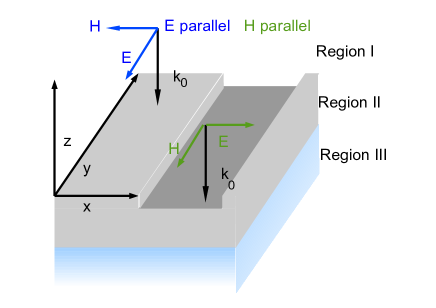
We split the diffraction problem into regions I-III, as shown in Figure 1, using the polarization convention denoted there. We denote as either for E parallel polarization or In region I, we study the case of perpendicular incidence, that is the incident light can be written as , and for both region I and III, the outgoing light can be written as a superposition of plane waves, i.e. and respectively, where , and . Region II contains the diffraction grating consisting of layers , each thick, and where refers to the layers position within the grating.
II.2 Grating Problem
As we confine our study to perpendicular incidence, we note that the fields and do not depend on y. Within Region II, we briefly note that within each layer the fields can be written as a sum of products , which permits a separation of variables, leading to the Helmholtz equation to be solved within a grating layer. Because is piecewise constant, the Helmholtz equation can be written piecewise, where we limit ourselves to two domains of constant permittivity. Hence,1 refers to domain one and 2 refers to domain two:
| (1) | |||||
| (2) |
where and are the domain-wise eigenfunctions and are the eigenvalues of the Helmholtz equation. The domain-wise eigenfunctions need to fulfill a set of boundary conditions at interfaces in addition to the eigenvalue equations, that is
for E parallel polarized light, and
for parallel polarized light.
With an eigenfunction composed of and we write the field as a sum of modes propagating between the adjacent layers,
| (3) |
where .
Then the Helmholtz equation together with the sets of basisfunctions and the additional constraint of boundary conditions between the patches define the numeric eigenvalue problem for the layer to be solved. This method allows to calculate a freely selectable number of eigenvalues and eigenfunctions to a precision limited by machine number size because of its exponential convergence. That is, within a grating layer, our eigenmodes are obtained to the same precision as in an analytic calculation following references by Botten et al. (1981c, a, b). Note that the symmetry at perpendicular incidence together with the symmetry within the grating layer result in either purely symmetric or antisymmetric functions, that is we only need half the number of variables, and therefore the symmetric eigenvalue problem requires only of the numerical effort as it scales with the number of variables to the third power, and for symmetric structures, this property carries over to the solution of the radiation condition boundary value problem. To this end, we follow (Morf, 1995) and, in addition, by using a minimum bandwidth banded matrix implementation that will be explained in detail in an upcoming publication.
At the interface between grating layers, the field or has to satisfy the following continuity equations
and the fact that within each layer there exists a different set of eigenmodes, means that a high number of modes have to be used to calculate the behaviour at such interfaces - regardless of the numeric method used.
The substantial reduction in modes through symmetry together with the implementation of the boundary value problem allows us to achieve the high resolution we need to describe both the spectra of such structures and their absorption properties.
II.3 Material Specific Absorption
To calculate the absorption within a lamellar slab, we make use of the Poynting vector along the boundary of a region containing the material for which the absorption needs to be known. The time-average of the Poynting Vector is given by (Born and Wolf, 1999)
It represents the directional energy flux density of the electromagnetic field.
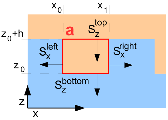
Assuming the Poynting vector is known for all the absorption in an area with border becomes . For a one-dimensional grating and non-conical incidence in the xz-plane, the electromagnetic field does not depend on and the integration in the y-direction can be omittted. For both polarization, the Poynting vector will have non-zero and components, i.e. . The absorption in the area can then be written as
For E (H)-polarisation, only ( is non-zero. Using Maxwell’s equation, the Poynting vector can then be written as
for E- and H-polarization, respectively. For both polarization the field or and its derivative can be written as
Without loss of generality, the coordinate can be set to . Then, at or , the integrated contribution of the Poynting vector in -direction becomes
where
is evaluated at the boundaries of the corresponding domain , respectively. Here and in the following, we drop the common factor in the expression for the Poynting vector. Since all absorption results will be quoted as a ratio with respect to the Poynting vector of the incident radiation, this factor would drop out anyway.
The contributions from the Poynting vector in z-direction at the top and bottom integrated with respect to , are quite easy to compute since the overlaps can be expanded in terms of products of Legendre polynomials that are orthogonal when integrated over a given domain consisting of the material for which the absorption has to be computed.
Thus only diagonal terms in the Legendre expansion of and survive, and the corresponding matrix can be evaluated as soon as the Legendre expansion coefficients of the eigenfunctions are known. Note how much more cumbersome such a calculation would be if instead of the Legendre basis a Fourier basis had been used. Then no orthogonality relation would exist for a single domain.
III The set of geometric structures
Here, we wish to present the structures which will be calculated in the following sections. The goal of these calculations will be to obtain the spectra of absorption in amorphous silicon and in the other absorbing materials, i.e. silver, aluminum, zincoxide and indium tin oxide, where absorption does not contribute to the generation of electron-hole pairs and should be kept as small as possible.
The first two structures are following the standard structure for amorphous silicon solar cells. They are formed by deposition of zinc oxide on a metallic reflector. Subsequently, amorphous silicon is deposited and last an indium tin oxide layer is deposited as a transparent contact. We ignore the fact that the amorphous silicon layer consists of three parts, n-doped - intrinsic and p-doped and consequently the absorption in the doped parts, that will not contribute to the photovoltaic efficiency.
a) b)
b)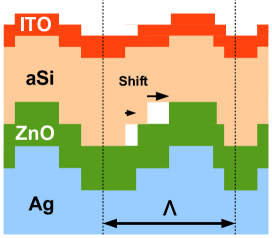
c)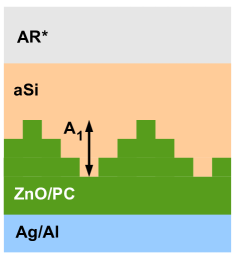 d)
d)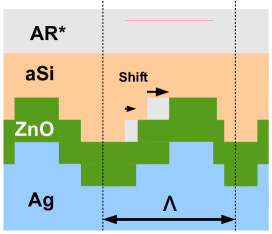
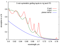
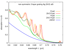
In the first two structures, Fig. 3a and 3b, the grating structure of the substrate, Ag in Fig. 3a and ZnO or polycarbonate in Fig. 3b, is reproduced in all subsequent layers which are deposited on the substrate, albeit with a somewhat reduced amplitude above the homogeneous a-Si layer, leading to some antireflection effect at the top of the structure. Fig. 3c and 3d show structures with a planar top a-Si surface and some artificial antireflective coating AR* which suppresses reflection. It is used in order to confine the investigation to the optimisation of light-trapping, cf Appendix, and study the benefits and deficiencies of structures 3c and 3d.
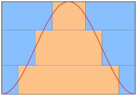
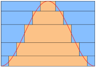
In addition, we also show how we approximate smooth surface relief gratings for the case of a sinusoidal profile in Fig. 4. For illustration purpose, we show 3 and 5 step versions. In this construction, we make use of a variable step height and step position in the horizontal direction, such that excess areas (yellow triangles above the sine) and missing areas (blue triangles below the sine) compensate exactly and at the same time the sum of the excess areas is minimized, while the sum of missing areas is minimized as well. This leads to a unique solution for any given number of steps, maintains the symmetries and the amount of material exactly. We will see below, that for increasing number of steps, the absorption spectra change very little.
For brevity, we will denote structures consisting of combinations of such materials and gratings as , where we start from left with the substrate, and where the pseudosine contains the materials and .
IV Results
Spectrally Integrated Absorption
For our calculations of integrated absorption, the following reference data should be kept in mind: The photon AM1.5 spectrum integrated from 380-770 nm counts as 100%, and a flat structure with a silver back reflector covered by an optimal layer of 50nm ZnO, 200nm a-Si and 60nm ITO on top absorbs 51% in the a-Si layer at perpendicular incidence. The contribution integrated from the wavelength range 550-770nm is about 19%. The cut-off wavelength of 380nm is determined both by the solar spectrum AM1.5 and by the very small decay length for photons below 400nm wavelength, such that the quantum efficiency becomes quite small. The upper cut-off wavelength of 770nm must be regarded as an upper limit for amorphous silicon whose band gap is between 1.6 and 1.7 eV, unless it is alloyed with germanium as is used in some amorphous silicon tandem cells.
| spectral range | a-Si|AR* | Ag|a-Si|AR* |
|---|---|---|
| 380-770nm | 0.97727 | 0.55247 |
| 380-550nm | 0.35589 | 0.35241 |
| 550-770nm | 0.62138 | 0.20006 |
| 600-770nm | 0.48215 | 0.08891 |
IV.1 Validity of our calculations
IV.1.1 Convergence of spectra for increasing number of modes
In this section, we present a few tests concerning the reliability and validity of our calculational method.
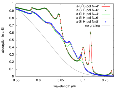
The first test is with a 7-step grating mimicking a sine grating (“7-step pseudo-sine”) 4 in a silver substrate with a total amplitude (peak to valley) of 64nm and a grating period of 586nm. Figure 5 we show that even the difficult case of a 7-step metallic pseudo-sine grating can be calculated reliably using a limited number of modes. For E-polarization, using 41 numerically exact modes are sufficient to calculate the spectrum accurately. For H-polarization, 61 numerically exact modes are required for H polarization, where the spectrum becomes virtually indistinguishable from a spectrum with 81 modes. Note the small deviation in the result for H-polarization around 630-670nm and close to 700nm wavelength. We will see below, that the absorption in silver is less well behaved.
IV.1.2 Energy conservation
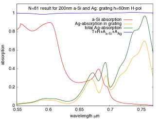
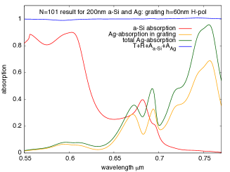
Another interesting test is provided by the requirement of energy conservation. Indeed, the sum of absorption in the different absorbing materials together with total reflection and transmission probabilities has to be close to unity if the calculations can be trusted. Here, we show the results of a particularly difficult calculation consisting of a square wave grating in a Ag substrate with height 60nm onto which an amorphous silicon layer of 200nm thickness is conformally deposited, thereby leading to a second square wave grating in Si and vacuum with the same height 3a) without ZnO and ITO.
In Figure 6 we observe a number of interesting features: (i) Huge parasitic absorption in the Ag grating for wavelengths above 700nm (yellow line) and also a growing contribution from the substrate absorption (green line). By contrast, in this spectral range the absorption in a-Si is very weak. (ii) Comparing the results of N=81 and N=101 modes, we observe that the main difference occurs in the absorption of Ag above about 720nm wavelength. This observation is consistent with the findings of Popov et al. (Popov et al., 2002)that the convergence of stair-case approximations to smooth metal surfaces is poor or even a serious problem. (iii) The spectrum of absorption within the amorphous Si (red line) is basically unchanged when the number of modes is increased. (iv) The energy conservation (blue line) is very stable and close to unity even at wavelengths where resonances are visible.
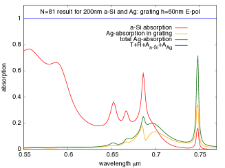
For the same structure, we also show the results for E-polarization. In this case, the differences between N=81 and N=101 modes are invisible on the scale of the plot. Both absorption in a-Si and Ag are quite a bit lower that in H-polarization. The parasitic absorption in Ag shows much narrower resonances, presumably due to much coupling between different modes. Energy conservation is even better behaved than in H-polarization in spite of the strong and sharp absorption resonances.
IV.1.3 Sinusoidal gratings mimicked by stair case gratings:
convergence in the number of steps
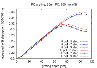
We now turn our attention to the behavior of the absorption spectra of “pseudosine” gratings, when the number of steps is increased. The structure corresponds to the one of Fig.3d) with a grating shape of 4. The spectral results 8 show that both for the grating in silver (left panel) as well as for the grating in PC, the results are quite insensitive to the number of steps even for H-polarization and a grating with the dangerous interface between silver and amorphous silicon. Indeed, the difference between 7 and 9 steps is negligeable in all cases, while the 5-step result shows the same qualitative features, maxima occurring at the close to same grating height. Looking more closely at the result for H-polarization in the left panel, we see that the absorption is somewhat lower for the 5-step grating, while in all other cases the 5-step grating leads to somewhat higher values.
We also abserve a qualitative difference between the results for the two polarization: While in both cases E-polarization does not decrease for larger grating height, H-polarization show a distinct maximum. For the silver grating, this maximum occurs already at around 50nm height, while for the polycarbonate (PC) grating it is around 80nm. We have seen in the case of Fig. 6 that the absorption in a silver-silicon grating becomes very weak, while the absorption in the metal becomes very large. This is consistent with the observation of a decreasing absorption as the grating exceeds a certain height. We have also tested this structure replacing silver by aluminum. The light-trapping effciency is only very little impacted by the small additional absorption in aluminum. The choice of PC is motivated by this consideration, but also because a planar substrate with a PC coating that is prestructure could be used in a straightforward way, even for mass production. How the contacts could be made in such a device remains an experimental problem.

IV.2 Plasmons at Material Interfaces
In reference (Sheng et al., 1982), it was mentioned that complex conjugate eigenvalues can occur in gratings with real, negative permittivities for H polarization, and this non-obvious property was rediscovered in references (Foresti et al., 2006; Sturman et al., 2007). Furthermore, in weakly absorbing materials, these eigenvalues are not exactly conjugate anymore, but they still occur pairwise. To obtain an accurate calculation, both eigenvalues must either be included or omitted. However, for the type of metallic structures studied in this paper, degenerate eigenmodes can occur as well. It is difficult to obtain these eigenvalues correctly with the modal method based on the transcendental equations, because these eigenmodes have nearly exactly degenerate eigenvalues, and are difficult to locate and especially find them both.
Using the polynomial method, they are quite easy to find. But, the fact that they occur in nearly degenerate pairs was initially a puzzle and unexpected. Only after testing these eigenvalues and eigenfunctions by looking at their convergence properties as the Legendre basis becomes very large, have we been convinced that they are no mere artefact of the polynomial method. And if the eigenvalues are known accurately, one can confirm that they are also solutions of the transcendental equation (Botten et al., 1981a, b; Sheng et al., 1982). These eigenfunctions display the character of plasmons. That they are nearly degenerate and for some wavelength numerically exactly degenerate is the result of their exponential decay away from the interface. If the two interfaces are sufficiently far apart, the tunnel splitting (in the language of quantum mechanics) becomes exponentially small. At zero angle of incidence, they can be classified by symmetry. As the geometry of a square wave grating with only two materials has axes of reflection symmetry, the eigenfunctions for perpendicular incidence can be eigenfunctions of the parity operator. If however the degeneracy is numerically exact, generally we will see superpositions of the two eigenvectors with undefined parity. In our example depicted in Fig. 9, the square wave grating consists of silver and amorphous silicon with a period 511nm and both materials with equal width. The wavelength is 670nm.
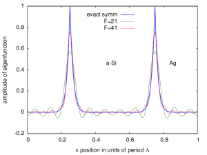
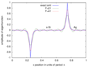
These plasmonic eigenfunctions appear as a result of the boundary conditions at the interface. In other words, the condition of enforces a sharp cusp in the magnetic field at the interface for H polarization, i.e. if the permittivities in different domains have the opposite sign. They cannot appear for E polarization, where the derivative of the field has to fulfill .
Figure 9 shows these eigenfunctions as well their Fourier approximations. The Fourier approximation was calculated as a series expansion of the eigenfunction as calculated from the corresponding numerically exact eigenfunction. The maximum value of the Fourier approximated eigenfunction clearly remains below the numerically exact maximum, and this Gibbs phenomenon leads to a significant underestimation of the maximum field value of the field. More importantly, at the cusp, the derivative of the exact eigenfunction is very large, whereas for any Fourier expansion based method the electric field component for vanishes at the interface, which is clearly wrong. Correspondingly, the current at the interface will vanish as well and thus the absorption near the surface will be significantly underestimated.
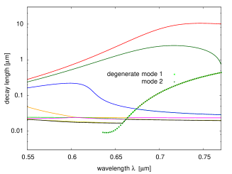
Figure 10 shows the mode spectrum of the modes with longest decay length. The degenerate modes start with very short decay length of less than 10nm around a wavelength of 640nm. The decay length is is a measure how far a mode can couple in the z-direction. With increasing wavelength above 680nm, the two degenerate plasmonic modes become propagating within the grating layer as its thickness is at most around 100nm. In the spectral range from 680 to 770nm they are the third and fourth most important modes carrying the energy flux. They do contribute to the absorption in the metal seen in Fig.6 and 8, which gets very large in H-polarization. Clearly their omission from a modal calculation would give wrong results. As they are very difficult to locate in the complex plane, the calculation of these eigenvalues and eigenfunctions is extremely difficult if we follow the treatment of refs. (Botten et al., 1981a, b; Sheng et al., 1982). By contrast, using the method of polynomial expansion of ref. (Morf, 1995), they are found directly and without missing modes ordered according to their number of nodes and up to a maximum number of nodes with a required precision which determines the necessary size of the polynomial basis.
2010 Gundu and Mafi reported an apparent non-convergence for the spectra of lossless metal gratings as calculated with modal methods (Gundu and Mafi, 2010a), and reported a method to reduce the problem in (Gundu and Mafi, 2010b). Li and Granet revealed the role of edge and hyper-singularities for such gratings in (Li and Granet, 2011; Li, 2012, 2014), and Mei, Liu and Zhong proposed a method that gradually varied the index of refraction over the boundary region in (Mei et al., 2014). While the silver back-reflector in solar cells is not lossless, it is highly conducting nevertheless, and remains a delicate calculation, given that the skin depth of the metal for the studied wavelength range of nm is on the order of 10nm. This skin depth of course also sets a minimum resolution requirement for numerical solution.
IV.3 Depth Dependence
In this section, we would like to give a short overview of the influence of several grating parameters on the absorption in the amorphous silicon part of the pseudo-sine gratings described above. Here and in the following, we wish to point out, that when the grating depth is varied, the total amount of amorphous silicon is always kept constant. This is done by reducing the thickness of the homogenous amorphous silicon layer. The reason for this choice is that we do not want to mix the effects of absorption by light-trapping with those resulting from modifying the total amount of silicon present in the structure.
IV.3.1 Amorphous Silicon Thickness and Grating Depth
The first grating parameter that can be investigated is the silicon thickness. For that, consider the first case of a silver grating case, where the total silicon thickness is gradually reduced. The left panel of figure 11 shows that for E polarization, the a-Si thicknesses nm have very little influence on the integrated absorption curve for grating depths between nm and nm. For H polarization, the right panel of figure 11 shows that the integrated absorption decreases for all grating depths with decreasing a-Si layer thickness.
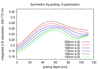
Figures 12 show that contrary to intuition, the integrated absorption contributions for 550-770nm for a simple square-wave grating are not just increasing for increasing a-Si layer thickness, but rather that there is a pronounced maximum at about 150nm, i.e. substantially below the 200nm thickness that is often the preferred choice in experiments.
IV.3.2 Polycarbonate Thickness
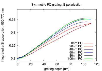
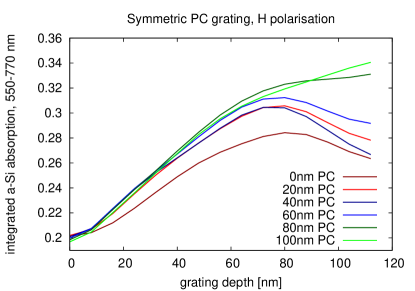
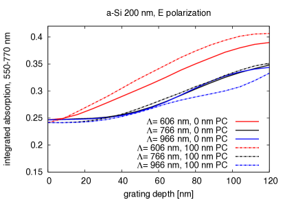
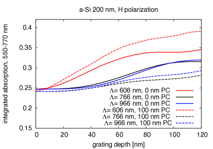
For the second case of a polycarbonate grating, the homogeneous polycarbonate layer thickness can be varied, as shown in figure13. The left panel of figure 13 shows that for E polarization there is an almost linear relationship between the grating depth and the a-Si absorption, and the spread between the PC layer grating thickness sets in gradually. For the H polarization shown in the right panel of 13 a thicker PC layer increases the absorption only very little for grating depths below 60 nm, whereas the absorption increases significantly with the nm and nm layers for gratings with a depth greater than nm.
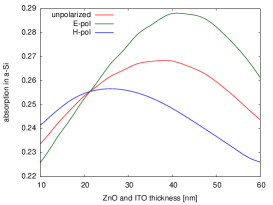
IV.3.3 Dependence on thickness of ZnO and ITO
In figure 14, we depict the behavior of the absorption as function of thickness of the ITO and ZnO layers. Clearly, the optimal values are quite different for the two polarization.
IV.4 Period Dependence
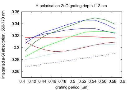
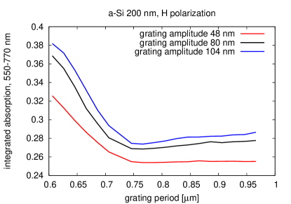
The influence of the grating period on the absorption is another parameter that can be studied. For that, consider the case of a ZnO grating on an aluminum substrate with 200nm amorphous silicon and an ideal antireflection layer on top of the silicon. The calculations for figures 15 and 16 were performed with 31 numerically exact eigenmodes. For H polarization, the right panel of figure 15 shows that the optimal period for maximal absorption in the amorphous silicon does not change, and that in the region of the optimal period the deepest gratings perform best. For E polarization, there is a material specific absorption optimum below the deepest structure with the largest period. This local optimum moves from about for a grating depth of nm to about for a grating depth of nm.
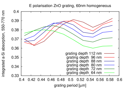
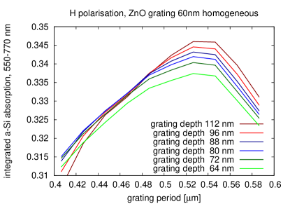
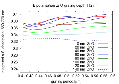
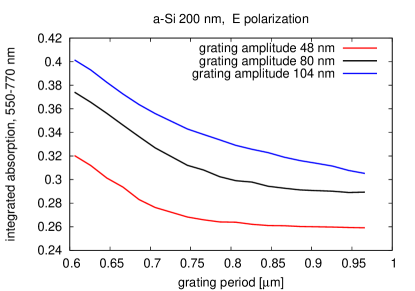
Figure 16 shows the period dependence of the integrated absorption for various thicknesses of the homogeneous ZnO layer below the ZnO grating. Both panels show that the ZnO layer thickness has a much stronger influence on the absorption than the period. The left panel shows that the optimum homogeneous ZnO layer thickness should be around nm for E polarization, and the right panel shows that for H polarization, the optimum thickness should be around nm.
IV.5 Larger Periods
So far, all investigated gratings have been using periods in the nm period range. This section will show that larger periods will not lead to an increase in absorption in the nm wavelength range. For this exploration, the example grating structure consisted of a flat silver back reflector, covered by a 7-step pseudo-sine polycarbonate grating which is covered with a silicon layer that is on average nm thick and flat on top. The grating is illuminated perpendicularly. The choice of a flat reflector at the bottom should be at the upper end of the attainable absorption for the amorphous silicon, given that it was shown section IV.A.2 that a substantial amount of absorption takes place in the metallic grating.
In figure 17, the depth dependence of the integrated absorption as a fraction of the AM1.5 spectrum is shown, and in figure 18 the period dependence is shown for select grating depths. Figure 18 clearly shows that periods above 600nm are not helpful to increase absorption in the chosen spectral region for both polarization, although the effect appears to be more drastic for H polarization. Figure 17 shows that increasing the homogeneous polycarbonate layer between silver and amorphous silicon does not increase absorption for the gratings with longer periods, but it may do so at nm and below. In all cases, deep gratings increase the absorption the most, however for real applications, their depth would have to remain limited for several reasons, including the manufacturing process and the need to establish electrical contacts. In figure 18, the homogeneous polycarbonate layer thickness is nm. The calculation presented made use of 31 modes in each layer.
IV.6 Improving metallic gratings by intermediate dielectric
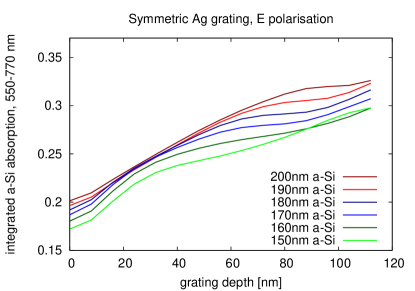
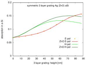
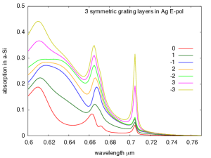
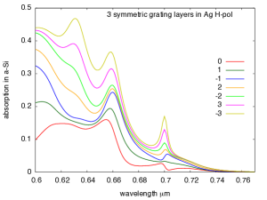
In section IV.1.2, we have observed the significant absorption occurring in a (silver | a-Si) grating. Here, we examine if the losses can be reduced by inserting a ZnO layer between silver and a-Si, i.e. by using instead (silver | ZnO | a-Si) inside the grating. That this can be successful is shown in Figure 19 for a symmetric 3-step pseudo-sine with period 566.1nm. The integrated absorption for 600770nm, AM1.5-weighted, shows that the ZnO lining of width 11nm on either side of the silver domain while reducing the silver width by 20nm improves the absorption in H-polarization for larger grating depth by about 16 percent. In E-polarization, the absorption is virtually unchanged. While the absorption in E-polarization steadily increases with increasing grating depth, in H-polarization it shows a maximum around a depth 50nm (unlined) and around 70nm with ZnO lining of width 11nm.
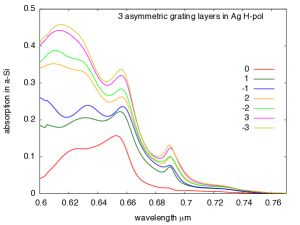
IV.7 Improving absorption by asymmetric gratings
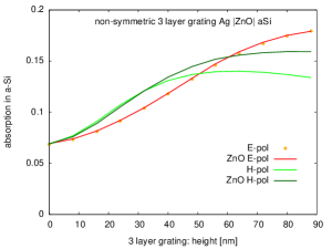
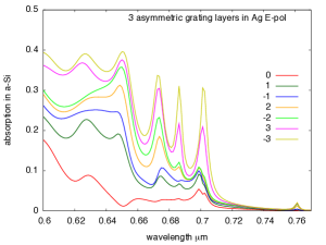
Here, we examine the effect of introducing geometric asymmetry in the 3-step pseudo-sine of section IV.6, by shifting the the layers forming the 3-step pseudo-sine of Fig. 19 by 0, 12 and 24 percent in units of the grating period =566.1nm, respectively. Qualitatively the behavior is not different from the symmetric grating case. Quantitatively, we observe that in the non-symmetric structure the absorption in E-polarization is increased by about 15 percent, while for H-polarization it is increased by only about 6 percent, when compared to the corresponding symmetric results of Fig. 19.
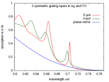
For completeness, we also show the spectra corresponding to the gratings structures of Figures 19 and 20 as well as a comparison between ZnO-lined and unlined spectra for the non-symmetric case. We can see that introducing asymmetry gives rise to additional peaks in the absorption spectrum, which in H-polarization are only present if the metal-semiconductor interface is modified by an intermediate ZnO layer (right panel). For E-polarization, the effect of the ZnO lining leads to a slight shift in the position of the peaks with no effect on their height and very little effect on their area.
IV.8 Absorption By Specific Modes
The question which modes contribute most to the absorption in a specific layer can be answered as well. To that end, the following method has been used: First, the full boundary value problem needs to be solved, together with the calculation of the local absorption in the chosen layer by calculating the surface integral of the Poynting vector, as shown in section II.3. Then, the calculation is to be repeated, while omitting the eigenmode of the chosen layer. The contribution of the eigenmode to the Poynting vector becomes where can be evaluated as Here, the and Fields can be evaluated as shown inII.3, and and are the electromagnetic fields calculated by not including the eigenmode.
Here, we examine the absorption within the homogeneous amorphous silicon layer, in which the modes are just the plane wave solutions appropriate to the dielectric properties of a-Si. The structure is the asymmetric grating with 11nm ZnO lining illustrated in the middle panel of Fig. 21 and with the structure defined in Fig. 19.
In the figures 22-23 the lowest of these modal contributions are shown for the case of a homogeneous a-Si layer on top of a 3-step pseudo-sine grating. Given that a homogeneous layer is analyzed, the eigenmodes are plane waves and numbered according to their Fourier order. In the figures shown, the modal contributions are consecutively added and plotted on top of each other. These modes account for 94-99% of all absorption within the layer such that the curve corresponding to the mode of order -3 becomes indistinguishable with the curve of the full boundary value problem, hence the total is not shown. Despite the fact that for all cases shown 7 modes suffice to calculate most of the contributions to absorption within the layer, the higher order modes are needed to calculate the boundary value problem accurately, and for the following calculations, 31 numerically exact modes in each layer were used.
Figures 22 and 23 show the modal contributions for E-polarization and H-polarization respectively on a symmetric and non-symmetric grating, and it can be seen that modes of equal number contribute an equal amount for both polarization. Furthermore, it is worth noting that throughout the spectrum, many modes contribute significantly to the absorption, whereas the resonance above shows a more dominant contribution of the mode for the absorption. In contrast, a similar resonance exists for H-polarization, where multiple modes contribute to the absorption.
Figures 22 (right panel) and 23(right panel) show the modal contributions for E-polarization and H-polarization respectively on an non-symmetric grating with the same grating parameters as above, but where all grating layers are shifted by with respect to neighboring layers, such that the resulting grating shows a significant asymmetry. Correspondingly, the modes of equal number do not contribute equal amounts to the absorption. For E-polarization the spectrum shows multiple resonances, where some modes contribute visibly more than others. In particular, the resonances above and above seem to have a significant contribution from the modes of order , however throughout the spectrum the other modes contribute visibly. For H-polarization, there are less visible resonances, and around the background absorption begins to drop. There, the relative contribution of the mode of order +1 becomes the dominant contribution, until about , where the total absorption becomes insignificant altogether.
V Discussion
In this paper, we have first developed an accurate and efficient method to calculate the material specific absorption with our numerically exact modal method. The accuracy of the solution is determined solely by the truncation order N, once the eigenvalues and eigenfunctions are ordered according to their relevance.
The criteria for the validity of calculations are convergence as the truncation order is increased, and we calculate the energy conservation and convergence with respect to the approximation of a given smooth surface profile, for which stair-case approximations are made.
For H-polarization, we have observed large parasitic absorption in metallic gratings in the spectral range in which the absorptivity of the semiconductor is weak. We trace this back to large currents close to the interfaces between metal and semiconductor. Indeed, we have found two-fold nearly degenerate eigenvalues of the Helmholtz equation for such gratings in an extended spectral range, and even numerically exactly degenerate for a specific wavelength. At normal incidence, the associated eigenfunctions are either symmetric or antisymmetric. They are localized at the position of the metal-semiconductor interface and decay exponentially away from it. Thus their degeneracy follows as the tunnel splitting will decay also exponentially as a function of the separation of the two interfaces.
Based on the presented findings, we attribute a significant part of these difficulties to interface plasmons and all modes that are responsible for large currents at and close to interfaces between metals and semiconductors. These currents are the source of the large parasitic absorption in even the metals with the smallest imaginary part of the dielectric constant, e.g. silver. For this reason, the ideal limit of absorption-free metals is so unrealistic that it is of no interest for photovoltaics.
We briefly summarize the most important findings of this work: Light-trapping can be improved by optimizing grating depth and period, by introducing an asymmetry which allows a coupling between modes of even and odd parity, effectively doubling the mode space. Asymmetry is found to be more effective for E-polarization. For some grating structures, it is found that the absorption in the semiconductor can increase significantly when its thickness is somewhat reduced. The analysis of the contribution to the absorption in the semiconductor of individual modes shows that a number of modes is of nearly equal importance even near and at resonance peaks in the spectrum. Finally, we find that the parasitic absorption in a metal-semiconductor grating can be reduced by insertion of a rather thin layer of a dielectric, in our case of the order of zinc-oxide of 10nm width.
In view of all these results, it is unclear to us, whether we can expect much better light-trapping performance from two-dimensional metal gratings. In that case, all polarizations will suffer from the problem of large interfacial currents and consequently enhanced parasitic absorption as we observe in one-dimensional metal gratings in H-polarization.
On the other hand, two-dimensional gratings between dielectric and semiconducting materials may well turn out superior. Modal calculations allowing a fairly exhaustive investigation of such structures will help to answer this question.
VI Acknowledgments
We acknowledge the financial support of this work by the Swiss Federal Office of Energy, and by the Paul Scherrer Institute. We also would like to thank F.J. Haug and H.P.Herzig for helpful discussions and advice, and E. Barakat and G. Smolik for reference calculations.
VII Appendix
Dispersion Fits
For polycarbonate, a refractive index of was used in the calculations.
Whenever noted in the grating calculations, a fit function was used to parametrize measured data. In particular, for the amorphous silicon, the dispersion data was supplied by Franz-Josef Haug, and the following fit functions were used for parametrization:
where and are fitted by polynomials
| a-Si | ZnO | ITO | Ag | Al | ||||||
|---|---|---|---|---|---|---|---|---|---|---|
| f0 | 0. | 40404338 | 1. | 70771866 | 1. | 21219668 | 2. | 29527609 | -2. | 26656817 |
| f1 | 7. | 66872671 | -4. | 37318385 | -2. | 14526761 | -19. | 04662349 | 3. | 19251777 |
| f2 | -15. | 06785446 | 6. | 12742066 | 2. | 91527508 | 26. | 97072796 | 2. | 33399365 |
| f3 | 8. | 73093040 | -2. | 98521339 | -1. | 78130071 | -12. | 13112197 | -1. | 43428367 |
| g0 | 19. | 65451137 | 184. | 89403859 | -10. | 55809870 | -3. | 25349091 | -3. | 09108230 |
| g1 | -107. | 24524864 | -1’331. | 94129402 | 18. | 52031840 | 16. | 14691273 | 29. | 11819344 |
| g2 | 210. | 41585170 | 3’398. | 09758613 | -17. | 55613183 | -19. | 20517240 | -70. | 78995115 |
| g3 | -153. | 50212937 | -3’794. | 48410470 | 7. | 49002208 | 8. | 36374561 | 82. | 73715473 |
| g4 | 0. | 00000000 | 1’570. | 98004140 | 0. | 00000000 | 0. | 00000000 | -36. | 92328757 |
In Table 1, we list the fitting parameters which assume that the wavelength is measured in micrometers for all materials, that are used in the present study of light-trapping performance.
Anti-Reflective Coating
For many calculations in this thesis, optimum limits for the absorption within the semiconductor layer are a goal. For a setting with light incident from the outside, reflection at the top surface must be suppressed to the extent possible. To do so, the following artificial antireflective coating was used in some calculations. This idealized cover almost completely eliminates reflection of the incident light at the top interface of the structure by introducing a homogeneous layer on top of the structure, which is made up of an artificial material AR* whose thickness is adjusted as a function of wavelength. This is clearly unphysical, but permits us to examine specifically light-trapping efficiency.
This material AR* is supposed to have a wavelength dependent refractive index , where is the refractive index of the layer below, and the symbol stands for the real part. If the antireflection coating is taken to have a thickness corresponding to , the reflections can be suppressed except at the ultraviolet and blue part of the spectrum, where amorphous silicon absorbs very efficiently. While this idealized device is unphysical, there are realizations of antireflective structures which lead to similarly low reflexion losses (Heine and Morf, 1995; Heine et al., 1996). The broadband antireflection structure described therein consists of a rectangular grating with an additional coating with a lower refractive index than the grating below. We did not want to introduce the complications resulting from having gratings with different period for antireflection and light-trapping. That such combinations will work in practice is certain. But it falls out of the scope of the present study.
Table of step height and positions for mimicking sine-grating by stair-case
| layer | 1 | 2 | 3 | 4 | 5 | |
| 1 | ||||||
Let , , and : then material I is in layer inside the interval ( and material II is in the remaining part of the interval (0,1).
References
- Mokkapati and Catchpole (2012) S. Mokkapati and K. R. Catchpole, Journal of Applied Physics 112, 101101 (2012).
- Yu et al. (2010) Z. Yu, A. Raman, and S. Fan, Proceedings of the National Academy of Sciences 107, 17491 (2010), http://www.pnas.org/content/107/41/17491.full.pdf+html .
- Haug et al. (2014) F.-J. Haug, K. Soderstrom, and C. Ballif, Photovoltaics, IEEE Journal of 4, 785 (2014).
- Haug et al. (2015) F.-J. Haug, K. Soderstrom, and C. Ballif, Photovoltaics, IEEE Journal of 5, 1534 (2015).
- Naqavi et al. (2011) A. Naqavi, K. Söderström, F.-J. Haug, V. Paeder, T. Scharf, H. P. Herzig, and C. Ballif, Opt. Express 19, 128 (2011).
- Isabella et al. (2013) O. Isabella, S. Solntsev, D. Caratelli, and M. Zeman, Progress in Photovoltaics: Research and Applications 21, 94 (2013).
- Botten et al. (1981a) I. Botten, M. Craig, R. McPhedran, J. Adams, and J. Andrewartha, Optica Acta: International Journal of Optics 28, 413 (1981a), http://dx.doi.org/10.1080/713820571 .
- Botten et al. (1981b) L. Botten, M. Craig, R. McPhedran, J. Adams, and J. Andrewartha, Optica Acta: International Journal of Optics 28, 1087 (1981b), http://dx.doi.org/10.1080/713820680 .
- Sheng et al. (1982) P. Sheng, R. S. Stepleman, and P. N. Sanda, Phys. Rev. B 26, 2907 (1982).
- Suratteau et al. (1983) J. Suratteau, M. Cadilhac, and R. Petit, Journal of optics 14, 273 (1983).
- Morf (1995) R. H. Morf, J. Opt. Soc. Am. A 12, 1043 (1995).
- Gablinger and Morf (2014) D. I. Gablinger and R. H. Morf, ArXiv e-prints (2014), arXiv:1407.6987 [physics.optics] .
- Botten et al. (1981c) L. Botten, M. Craig, and R. McPhedran, Optica Acta: International Journal of Optics 28, 1103 (1981c), http://dx.doi.org/10.1080/713820701 .
- Born and Wolf (1999) M. Born and E. Wolf, Principles of optics: electromagnetic theory of propagation, interference and diffraction of light (Cambridge university press, 1999).
- Popov et al. (2002) E. Popov, M. Nevière, B. Gralak, and G. Tayeb, J. Opt. Soc. Am. A 19, 33 (2002).
- Foresti et al. (2006) M. Foresti, L. Menez, and A. V. Tishchenko, J. Opt. Soc. Am. A 23, 2501 (2006).
- Sturman et al. (2007) B. Sturman, E. Podivilov, and M. Gorkunov, Phys. Rev. B 76, 125104 (2007).
- Gundu and Mafi (2010a) K. M. Gundu and A. Mafi, J. Opt. Soc. Am. A 27, 1694 (2010a).
- Gundu and Mafi (2010b) K. M. Gundu and A. Mafi, J. Opt. Soc. Am. A 27, 2375 (2010b).
- Li and Granet (2011) L. Li and G. Granet, J. Opt. Soc. Am. A 28, 738 (2011).
- Li (2012) L. Li, J. Opt. Soc. Am. A 29, 593 (2012).
- Li (2014) L. Li, J. Opt. Soc. Am. A 31, 808 (2014).
- Mei et al. (2014) Y. Mei, H. Liu, and Y. Zhong, J. Opt. Soc. Am. A 31, 900 (2014).
- Heine and Morf (1995) C. Heine and R. H. Morf, Appl. Opt. 34, 2476 (1995).
- Heine et al. (1996) C. Heine, R. H. Morf, and M. T. Gale, Journal of Modern Optics 43, 1371 (1996), http://dx.doi.org/10.1080/09500349608232810 .