Experimental realization of a topological p–n junction
by intrinsic defect-grading
Abstract
A junction between an n- and p-type semiconductor results in the creation of a depletion region whose properties are at the basis of nowadays electronics. If realized using topological insulators as constituent materials, p-n junctions are expected to manifest several unconventional effects with great potential for applications. Experimentally, all these fascinating properties remained unexplored so far, mainly because prototypical topological PNJs, which can be easily realized and investigated, were not readily available. Here, we report on the creation of topological PNJs which can be as narrow as few tenths of nm showing a built-in potential of 110meV. These junctions are intrinsically obtained by a thermodynamic control of the defects distribution across the crystal. Our results make Bi2Te3 a robust and reliable platform to explore the physics of topological p-n junction.
pacs:
The recent discovery of topologically protected surface states in the binary chalchogenides Bi2Te3 Chen et al. (2009), Bi2Se3 Xia et al. (2009) and Sb2Te3Jiang et al. (2012a) has tremendously revitalized the interest in these narrow gap semiconductors that have been studied for decades because of their excellent thermoelectric properties Venkatasubramanian et al. (2001). Topological insulators (TIs) are materials insulating in the bulk but metallic on their surface due to the existence of linearly dispersing gapless states which, contrary to the trivial surface states usually found in metals and semiconductors, are protected by time reversal symmetry Hasan and Kane (2010). The strong spin-orbit coupling characterizing these materials perpendicularly locks the spin to the momentum, resulting in a chiral spin texture which forbids backscattering Roushan et al. (2009); Zhang et al. (2009) and makes spin currents intrinsically related to charge currents König et al. (2007).
These unconventional properties make TIs an ideal platform to realize exotic states of matter, such as Majorana fermions Fu and Kane (2008) and magnetic monopoles Qi et al. (2009). Furthermore, they appear to be ideal candidates to realize magneto-electric and spintronics devices with low power consumption Garate and Franz (2010). Within this framework, the creation of p–n junctions (PNJ), which are the building blocks of several semiconducting devices, such as diodes, sensors, solar cells, or transistors, in topological materials would represent the first step towards the direct application of this fascinating class of materials Wang et al. (2012). In TIs, the massless character of surface carriers and the helical spin texture inversion at the p–n interface are predicted to result in several unconventional phenomena, e.g. gapless chiral edge mode Wang et al. (2012), Klein tunneling Katsnelson et al. (2006), Veselago lenses Cheianov et al. (2007), exciton condensation and charge fractionalization Seradjeh et al. (2009).
Experimentally, all these fascinating properties remained unexplored so far, mainly because prototypical topological PNJs, which can be easily realized and investigated, were not readily available. One issue towards the successful fabrication of topological PNJs is the presence of defects which are intrinsically incorporated in TI materials during the growth process. Thereby, the resulting TI crystals are heavily doped at a relatively high bulk carrier concentration level Scanlon et al. (2012); Wang et al. (2013). Since bulk carriers give rise to leakage currents that make capacitive charging impossible their existence represent a severe obstacle towards the creation of topological PNJs by applying a gate bias between opposite surfaces of a TI thin film Seradjeh et al. (2009).
Recent studies showed, however, that—depending on the growth conditions—large deviations from the nominal composition can be obtained Mi et al. (2013). These defects, which can be anti-sites or vacancies, are characterized by different formation energies. Here, we demonstrate that their inevitable presence can be turned into a positive effect by thermodynamically controlling their distribution across the crystal. In particular, we show how appropriate growth conditions result in the creation of bulk crystals that intrinsically contain topological PNJs at their surface, thereby avoiding the complicated fabrication of heterostructures and the problems related to the creation of interfaces between different materials Zeng et al. (2013); Zhao et al. (2013, 2014). Atomic scale scanning tunneling microscopy (STM) and spectroscopy (STS) measurements combined with ab initio calculations evidence that Te segregation Wang et al. (2011); Jia et al. (2012); Wang et al. (2013) results in well-separated Te- and Bi-rich regions that display p- and n-transport character, respectively. Spatially resolved Hall and Seebeck measurements confirm the transition from p- to n-like transport. At the p–n interface the oppositely charged defects, i.e. donors or acceptors, compensate, resulting in a substantial drop of conductivity by almost two orders of magnitude. Scanning tunneling spectroscopy reveals a built-in potential of about 110 meV, thereby considerably shifting the Dirac point in between the p- and n-region. Spectroscopic data obtained within the p–n compensation region indicate that the junction width amounts to several 10 nm only.
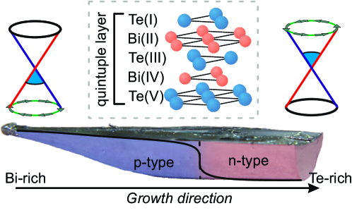
Figure 1 schematically presents some essential background information related to our approach. Within the hatched box of Fig. 1 the crystal structure of a quintuple layer of the binary chalchogenide Bi2Te3 is shown. It consists of alternating Te and Bi layers. Adjacent quintuple layers are weakly bound by van der Waals forces thereby offering a natural cleavage plane, a situation highly advantageous for STM experiments. The bottom panel of Fig. 1 shows a photographic image of a Bi2Te3 crystal grown by the modified Bridgman technique (see Experimental Section for details). The crystal has a nominal composition with a Te content of 61 mol%. As recently shown, the conduction of Bi2Te3 crystals changes from p- to n-type at approximately this Te concentration Kokh et al. (2014). Due to Te segregation, however, the stoichiometry will not be constant but continuously change during the growth process from Bi-rich to Te-rich, as indicated by different color shadings in the bottom panel of Fig. 1. Correspondingly, we expect Dirac points which are energetically located below and above the Fermi level, respectively, with opposite rotational sense of the spin polarization. As we move from p- to n-doped surface areas we expect to pass through a transition region with equal concentrations of Bi- and Te-induced charge carriers where the carrier concentration becomes minimal, thereby realizing an intrinsic TI.
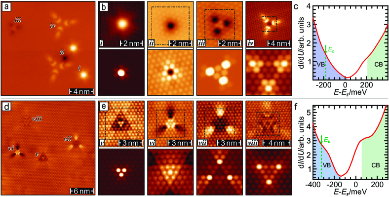
In fact, the differently doped areas can clearly be distinguished by STM and STS. Fig. 2(a) displays an overview topographic STM image obtained at the (0001) surface of the Bi-rich crystal region. Four different defects labeled (i)-(iv) are visible on the surface. Since the defects symmetry and extension reflects the perturbation introduced by the bonding structure within the crystal Jiang et al. (2012b) (see bond geometry sketched in the inset of Fig. 1), a detailed analysis of the atomically resolved images reported in the top row of Fig. 2(b) allows to identify their location within the quintuple layer structure of Bi2Te3, i.e. Te(I)-Bi(II)-Te(III)-Bi(IV)-Te(V), where Te(I,V) and Te(III) represent two inequivalent Te planes. Following this procedure the defects (i)-(iv) are all located within Te layers, and they can be Te vacancies (VTe) or antisites (BiTe). Due to the lack of chemical sensitivity of STM a definite assignment can only be achieved by a comparison of the experimental data with simulated STM images obtained from ab initio calculations [bottom row of Fig. 2(b)]. Based on the good general agreement achieved between the experimental and theoretical images we can make the following defect assignment: defect (i) is a BiTe(I) antisite; defect (ii) is a Te surface vacancy (VTe(I)); defect (iii) is a Te vacancy in the third layer (VTe(III)); and defect (iv) is a Bi antisite in the fifth layer (BiTe(V)). Since all defects are located in Te layers this region is expected to be Te-poor. This is confirmed also by theoretical calculations which show that these defects are characterized by the lowest formation energy in Bi-rich regions Scanlon et al. (2012). The electronic properties of this sample region can be characterized by an investigation of the local density of states as inferred by the STS spectra reported in Fig. 2(c). Following the energy level positioning scheme adopted in Ref. Sessi et al. (2013) we obtain a valence band maximum close to the Fermi level, thereby indicating the p-doped character of this sample region.
Investigation of the opposite side of the crystal reveals four other defects (v)-(viii) [Fig. 2(d)], the STM appearance of which is quite different from the data presented in Fig. 2(a)-(b) before. Again the symmetry and lateral extension of the various defects in atomic resolution data were used to estimate the position of the defects. Based on these estimations ab initio DFT calculations were performed. The comparison presented in Fig. 2(e) reveals a very reasonable agreement. Our results show that all four defects are located in the two Bi layers of the Bi2Te3 quintuple layer, in agreement with the expected Te-rich stoichiometry. Namely, the following assignments were concluded: defect (v) is a TeBi(II) antisite; defect (vi) is a Bi vacancy (VBi(II)); defect (vii) is a TeBi(IV) antisite; and defect (viii) is a Bi vacancy, VBi(IV). As for the p-doped region, our defects identification is consistent with the formation energies calculated by Scanlon et al. Scanlon et al. (2012), which show that in Bi2Te3 grown under Te-rich conditions the lowest energy defects are TeBi antisites and Bi vacancies, with the last ones playing a much less significant role. Comparison of the STS spectra shown in Fig. 2, panels (c) and (f), reveals that the different types of defects present in Bi- and Te- rich areas strongly influence the respective electronic properties, i.e. Te-rich regions show a rigid spectral shift towards negative energies with respect to Bi-rich areas. This negative shifts amounts to approximately 140 meV between the p- and n-doped surface areas of the Te-rich and Bi-rich parts of the crystal, respectively. This observation implies that a topological PNJ is naturally present within our crystals.
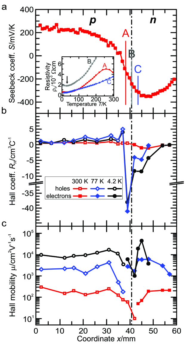
Figure 3(a) shows the room-temperature Seebeck coefficient of a Bi2Te3 single crystal measured at various positions (0–60 mm) along the crystal growth direction . It continuously and slowly changes along the crystal rod with a sign change occurring at a position of 35 mm. A positive Seebeck coefficient in the range of 250–100 V/K is obtained for the left part of the crystal boule (starting from ). Further right to this region, i.e. between 30 mm and about 35 mm, the Seebeck coefficient rapidly drops and eventually becomes negative, indicating that the crystal conductivity changes from p- to n-type at the point where V/K. In the region of the p–n transition (V/K) a potential Seebeck microprobe demonstrates the change of sign of the Seebeck coefficient on the 200 m distance, limited by the resolution of the method. At mm a high value V/K is obtained.
This interpretation is also corroborated by Hall measurements presented in Fig. 3(b) which were taken at the bottom and top parts of the boule. They show opposite signs of Hall coefficients , thereby confirming the presence of both p- and n-type regions. The left part of the boule (0–30 mm) shows metallic behavior with small positive Hall coefficients leading to a weakly temperature-dependent p-type carrier concentration, cm-3. At the right part a similar metallic-like behavior was observed for n-type carriers (cm-3). The large carrier concentration and its weak temperature dependence indicate that the bottom and top parts of the boule are heavily doped by acceptors and donors, respectively. Due to a strong reduction of the carrier concentration by two orders of magnitude ( cm-3) in the vicinity of the p–n junction, the Hall coefficient changes sign and drops down to cm3C-1 at low temperatures. These data indicate that an intrinsic binary chalchogenide TI can be obtained by a minimization of the carrier concentration through a careful control of the alloy composition between Bi and Te.
Electrical resistivity temperature dependencies were measured on the samples taken from positions A, B, and C [cf. Fig 3(a)], i.e. within a distance of 2 mm of the sign change of the Hall coefficient. In all the points resistivity decreases for temperatures from RT to K, and then remains almost constant down to the liquid helium temperatures for p- and n- type samples, while for point B resistivity increases, demonstrating semiconducting behavior. In both p- and n-parts of the crystal, the mobilities show a high average value of cm2V-1s-1 at low temperatures [Fig 3(c)]. At mm in the n-type region, i.e. close to the p–n transition, reaches the maximum value of about cm2V-1s-1. At the same position a maximum Seebeck coefficient V/K is observed, meaning that near the p-n transition there is the suppression of the defects formation.
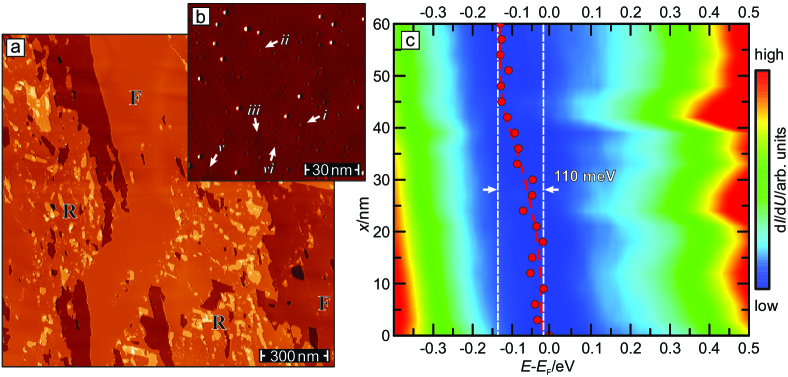
In order to investigate the minimal width of intrinsic TI p–n transitions that result from the slightly graded stoichiometry during the crystallization process, we have performed STM/STS in the zone where the transition was detected in the transport measurements described above. An overview scan is displayed in Fig. 4(a). While the surface region in the left and the bottom right part of the image is relatively rough (marked R) because of numerous small islands and clusters, we also find regions with extended atomically flat terraces separated by unit-cell step edges (F). As we zoom into such an atomically flat region [Fig. 4(b)] we can observe the coexistence of defects which we identify as being characteristic for n- and p-type Bi2Te3, i.e. defects (i), (ii), and (iii) as well as (v) and (vi), respectively (see above). This microscopic picture explains the drop of the Hall coefficient observed in transport, see Fig. 3 and Ref. Jia et al., 2012; Mi et al., 2013. It is also in agreement with the mobility drop detected in the p-n junction region, which can be thus be directly linked to the increased number of total defects. Overall, these findings have deep implications going beyond the scope of the present work. Minimizing bulk conductivity has always been considered as a powerful strategy to let topological surface states dominate the scene. However, it was not clear up to know if this effect should be ascribed to defects suppression or compensation. The combination of transport measurements with atomic scale characterization techniques provides thus a detailed microscopic picture solving this problem, identifying defect compensation as the responsible mechanism. Defect suppression can be safely ruled out since it would require a significant reduction of the defects concentration, a condition not consistent with our results.
Local spectroscopic data show that these regions contain several PNJs which are very sharp. This is corroborated by the color-coded STS data shown in Fig. 4(c) measured with a 3 nm increment along a 60 nm long line in a flat region. The minimum position is marked by a red dot in each spectrum. Indeed we observe a shift of the minimum from close to the Fermi level at nm to meV at nm, i.e. the transition from p- to n-doped Bi2Te3 takes place over the remarkably short distance of about 40 nm, although the p- or n-type character observed at the two ends of the boule [cf. Fig. 2(c) and (f)] is not fully reached.
Experimental data obtained on a larger length scale indicate that the doping gradient is not monotonic but exhibits some fluctuations which lead to the coexistence of several p–n transition regions. Their distance typically amounts to m, a value also matching the length scale of flat (F) and rough (R) surface patches in Fig. 4(a). Both behaviors potentially reflect the complicated convection processes that take place during the slow cooling and crystallization process of the boule. Their averaged random distribution result in a Ohmic characteristic preventing spatially averaging technique from verifying the existence of a rectifying behavior, an aspect which may be directly tackled by using nanoscale four probes techniques. Although their creation is not yet fully controlled, our data indicate that p–n transition regions naturally resulting from the slightly graded stoichiometry of crystals may be very narrow. Further research may lead to optimized procedures which better control their position and width to make them useful for application.
In summary, we demonstrated that, contrary to other materials, the ambipolar behavior of Bi2Te3 makes possible, by taking advantage of the intrinsic defects which are unavoidably introduced during the growth process, to create topological p–n junctions. Scanning tunneling spectroscopy reveals that their width amounts to 40 nm only. The related potential drop of approximately 110 meV shall allows for direct applications of PNJs in room temperature devices. Additionally, the defect compensation naturally achieved at the p–n interface results in a strong reduction of the bulk carriers concentration, thus paving the way to explore the PNJ topological properties.
I Acknowledgments
The authors gratefully acknowledge stimulating discussions with Mario Italo Trioni. This work was supported by the Deutsche Forschungsgemeinschaft within SPP 1666 (Grant No. BO1468/21-1). K.A.K. and O.E.T. acknowledge the financial support by the RFBR (Grant nos. 13-02-92105 and 14-08-31110).
II Experimental section
Bi2Te3 crystals have been grown by the modified Bridgman technique with a temperature gradient of about 10 K/cm at the front of crystallization Kokh et al. (2014). As-grown ingots had a single crystalline structure and were split into two parts along the cleavage plane (0001) oriented along the growth direction (Fig. 1). One part of each crystal was cut perpendicular to the growth axis into 0.5–1 mm samples. Indium solder Ohmic contacts were used for transport measurements. The Hall resistance and the resistance were measured in the Hall bar geometry using a standard six-probe method on rectangular samples. A potential Seebeck microprobe was used to investigate the room-temperature Seebeck coefficient in the region of p–n transition with a spatial resolution of 200 m. The Hall mobility was calculated from the measured conductivity and calculated carrier concentration, which was extracted from the measured Hall coefficient: n=1/(Rh*e). The carrier concentration dependence along the crystal was shown in Kokh et al. (2014).
STM measurements were performed at a tip and sample temperature K with electro-chemically etched tungsten tips. After transfer into the ultra-high vacuum system, samples were cleaved at room temperature at a base pressure mbar and immediately inserted into the cryogenic STM. The PNJ was located by bringing the tip into tunneling distance from the surface and recording a local tunneling spectrum indicative for p- or n-type doping [cf. Fig. 2(c) and (f)]. After retracting the tip the sample was moved with an -stage (initially by several tens to hundreds of m). This procedure was repeated until a spectral shift signaled that the boundary to the region governed by the other dopant had been crossed. Then a refined procedure with smaller -movements was performed.
III Theoretical calculation
Ab-initio theoretical calculations were performed by density functional theory, using a pseudo-potential representation of the electron–ion interaction and local orbital basis sets, as implemented in the SIESTA code Soler et al. (2002). We used a generalized gradient approximation (GGA) for the exchange-correlation functional Perdew et al. (1996) and a plane wave cutoff equal to 250 Ry. The experimental lattice constant for the hexagonal cell of Bi2Te3 was used Wang and Cagin (2007) and a surface cell was adopted to reduce the lateral interaction between crystal defects. The slab thickness was chosen in order to include three of the quintuple layers forming the building block of Bi2Te3 in the direction orthogonal to the surface and a large portion of vacuum of approximatively 30 Å. Constant–distance STM images have been simulated in the Tersoff-Hamann model Tersoff and Hamann (1985) by calculating the Kohn-Sham local density of states (LDOS) in the energy interval between the Fermi level and Donati et al. (2009), where the applied bias was fixed in agreement with the experimental setup. In particular the moderately large value of , of the order of 0.4 eV, allows us to obtain numerically stable results and to reasonably neglect the small inaccuracy of the LDOS around the Fermi level due to the absence of spin-orbit interaction in the calculation. A tip–surface distance equal to 3 Å was considered, although we verified that the result of our STM simulations are robust against small variations of this value. The extension of the tip was taken into account in the STM simulation by considering the mean value of LDOS within a radius of 4 Å around the tip position.
References
- Chen et al. (2009) Y. L. Chen, J. G. Analytis, J.-H. Chu, Z. K. Liu, S.-K. Mo, X. L. Qi, H. J. Zhang, D. H. Lu, X. Dai, Z. Fang, et al., Science 325, 178 (2009), eprint 10.1126/science.1173034.
- Xia et al. (2009) Y. Xia, D. Qian, D. Hsieh, L. Wray, A. Pal, H. Lin, A. Bansil, D. Grauer, Y. S. Hor, R. J. Cava, et al., Nat. Phys. 5, 398 (2009), eprint http://dx.doi.org/10.1038/nphys1274.
- Jiang et al. (2012a) Y. Jiang, Y. Wang, M. Chen, Z. Li, C. Song, K. He, L. Wang, X. Chen, X. Ma, and Q.-K. Xue, Phys. Rev. Lett. 108, 016401 (2012a), eprint http://link.aps.org/doi/10.1103/PhysRevLett.108.016401.
- Venkatasubramanian et al. (2001) R. Venkatasubramanian, E. Siivola, T. Colpitts, and B. O’Quinn, Nature 413, 597 (2001), eprint http://dx.doi.org/10.1038/35098012.
- Hasan and Kane (2010) M. Z. Hasan and C. L. Kane, Rev. Mod. Phys. 82, 3045 (2010), eprint http://link.aps.org/doi/10.1103/RevModPhys.82.3045.
- Roushan et al. (2009) P. Roushan, J. Seo, C. V. Parker, Y. S. Hor, D. Hsieh, D. Qian, A. Richardella, M. Z. Hasan, R. J. Cava, and A. Yazdani, Nature 460, 1106 (2009), eprint http://dx.doi.org/10.1038/nature08308.
- Zhang et al. (2009) T. Zhang, P. Cheng, X. Chen, J.-F. Jia, X. Ma, K. He, L. Wang, H. Zhang, X. Dai, Z. Fang, et al., Phys. Rev. Lett. 103, 266803 (2009), eprint http://link.aps.org/doi/10.1103/PhysRevLett.103.266803.
- König et al. (2007) M. König, S. Wiedmann, C. Brüne, A. Roth, H. Buhmann, L. W. Molenkamp, X.-L. Qi, and S.-C. Zhang, Science 318, 766 (2007), eprint http://www.sciencemag.org/content/318/5851/766.full.pdf.
- Fu and Kane (2008) L. Fu and C. L. Kane, Phys. Rev. Lett. 100, 096407 (2008), eprint http://link.aps.org/doi/10.1103/PhysRevLett.100.096407.
- Qi et al. (2009) X.-L. Qi, R. Li, J. Zang, and S.-C. Zhang, Science 323, 1184 (2009), eprint http://www.sciencemag.org/content/323/5918/1184.full.pdf.
- Garate and Franz (2010) I. Garate and M. Franz, Phys. Rev. Lett. 104, 146802 (2010), eprint http://link.aps.org/doi/10.1103/PhysRevLett.104.146802.
- Wang et al. (2012) J. Wang, X. Chen, B.-F. Zhu, and S.-C. Zhang, Phys. Rev. B 85, 235131 (2012), eprint http://link.aps.org/doi/10.1103/PhysRevB.85.235131.
- Katsnelson et al. (2006) M. I. Katsnelson, K. S. Novoselov, and A. K. Geim, Nat. Phys. 2, 620 (2006), eprint http://dx.doi.org/10.1038/nphys384.
- Cheianov et al. (2007) V. V. Cheianov, V. Fal’ko, and B. L. Altshuler, Science 315, 1252 (2007), eprint http://www.sciencemag.org/content/315/5816/1252.full.pdf.
- Seradjeh et al. (2009) B. Seradjeh, J. E. Moore, and M. Franz, Phys. Rev. Lett. 103, 066402 (2009), eprint http://link.aps.org/doi/10.1103/PhysRevLett.103.066402.
- Scanlon et al. (2012) D. O. Scanlon, P. D. C. King, R. P. Singh, A. de la Torre, S. M. Walker, G. Balakrishnan, F. Baumberger, and C. R. A. Catlow, Advanced Materials 24, 2154 (2012), eprint http://dx.doi.org/10.1002/adma.201200187.
- Wang et al. (2013) L.-L. Wang, M. Huang, S. Thimmaiah, A. Alam, S. L. Bud’ko, A. Kaminski, T. A. Lograsso, P. Canfield, and D. D. Johnson, Phys. Rev. B 87, 125303 (2013), eprint http://link.aps.org/doi/10.1103/PhysRevB.87.125303.
- Mi et al. (2013) J.-L. Mi, M. Bremholm, M. Bianchi, K. Borup, S. Johnsen, M. Søndergaard, D. Guan, R. C. Hatch, P. Hofmann, and B. B. Iversen, Advanced Materials 25, 889 (2013), eprint http://dx.doi.org/10.1002/adma.201203542.
- Zeng et al. (2013) Z. Zeng, T. A. Morgan, D. Fan, C. Li, Y. Hirono, X. Hu, Y. Zhao, J. S. Lee, J. Wang, Z. M. Wang, et al., AIP Advances 3, 072112 (2013), URL http://scitation.aip.org/content/aip/journal/adva/3/7/10.1063/1.4815972.
- Zhao et al. (2013) Y. Zhao, C.-Z. Chang, Y. Jiang, A. DaSilva, Y. Sun, H. Wang, Y. Xing, Y. Wang, K. He, X. Ma, et al., Scientific Reports 3, 3060 EP (2013), URL http://dx.doi.org/10.1038/srep03060.
- Zhao et al. (2014) Y. Zhao, H. Liu, X. Guo, Y. Jiang, Y. Sun, H. Wang, Y. Wang, H.-D. Li, M.-H. Xie, X.-C. Xie, et al., Nano Letters 14, 5244 (2014), pMID: 25102289, eprint http://dx.doi.org/10.1021/nl502220p, URL http://dx.doi.org/10.1021/nl502220p.
- Wang et al. (2011) G. Wang, X.-G. Zhu, Y.-Y. Sun, Y.-Y. Li, T. Zhang, J. Wen, X. Chen, K. He, L.-L. Wang, X.-C. Ma, et al., Advanced Materials 23, 2929 (2011), eprint http://dx.doi.org/10.1002/adma.201100678.
- Jia et al. (2012) S. Jia, H. Beidenkopf, I. Drozdov, M. K. Fuccillo, J. Seo, J. Xiong, N. P. Ong, A. Yazdani, and R. J. Cava, Phys. Rev. B 86, 165119 (2012), eprint http://link.aps.org/doi/10.1103/PhysRevB.86.165119.
- Kokh et al. (2014) K. A. Kokh, S. V. Makarenko, V. A. Golyashov, O. A. Shegai, and O. E. Tereshchenko, CrystEngComm 16, 581 (2014), eprint http://dx.doi.org/10.1039/C3CE42026D.
- Jiang et al. (2012b) Y. Jiang, Y. Y. Sun, M. Chen, Y. Wang, Z. Li, C. Song, K. He, L. Wang, X. Chen, Q.-K. Xue, et al., Phys. Rev. Lett. 108, 066809 (2012b), URL http://link.aps.org/doi/10.1103/PhysRevLett.108.066809.
- Sessi et al. (2013) P. Sessi, M. M. Otrokov, T. Bathon, M. G. Vergniory, S. S. Tsirkin, K. A. Kokh, O. E. Tereshchenko, E. V. Chulkov, and M. Bode, Phys. Rev. B 88, 161407 (2013), eprint http://link.aps.org/doi/10.1103/PhysRevB.88.161407.
- Soler et al. (2002) J. M. Soler, E. Artacho, G. J. D., A. García, J. Junquera, P. Ordejón, and D. Sánchez-Portal, J. Phys.: Cond. Matter 14, 2745 (2002).
- Perdew et al. (1996) J. P. Perdew, K. Burke, and M. Ernzerhof, Phys. Rev. Lett. 77, 3865 (1996).
- Wang and Cagin (2007) G. Wang and T. Cagin, Phys Rev. B 76, 075201 (2007).
- Tersoff and Hamann (1985) J. Tersoff and D. R. Hamann, Phys Rev. B 31, 805 (1985).
- Donati et al. (2009) F. Donati, P. Sessi, S. Achilli, A. Li Bassi, M. Passoni, C. S. Casari, C. E. Bottani, A. Brambilla, A. Picone, M. Finazzi, et al., Phys Rev. B 79, 195430 (2009).