Current developments in silicene and germanene
Abstract
Exploration of the unusual properties of the two-dimensional materials silicene and germanene is a very active research field in recent years. This article therefore reviews the latest developments, focusing both on the fundamental materials properties and on possible applications.
I Introduction
Graphene, a single layer of C atoms closely packed in a two-dimensional (2D) honeycomb lattice, exhibits intriguing electronic properties such as a very high carrier mobility Novoselov . The valence and conduction bands form a Dirac cone at the Fermi energy (zero gap semiconductor) with the electrons behaving as massless Dirac fermions, which can be useful in nanoelectronics Xu , for example. However, difficulties in the realization and tuning of a reasonable band gap currently are shifting interest from graphene to other 2D materials, such as -BN Watanabe ; Kubota ; Meyer , transition metal dichalcogenides Novoselov3 ; Geim2 ; sant1 ; sant2 , silicene sahin1 ; Fleurence ; datta ; Meng ; Xu ; Quaresima ; Chen , germanene Lia ; kaloni-jap ; NJP ; nano-2015 , and silica Ongun . Being composed of the group-IV elements Si and Ge, silicene and germanene immediately come into mind as alternatives to graphene. Silicene has been predicted theoretically by Takeda and Shiraishi in 1994 Takeda , re-investigated by Guzmán-Verri and co-workers in 2007 Voon , and confirmed to be stable by Cahangirov and co-workers in 2009 ciraci3 . Subsequently various groups have grown it on different Ag surfaces Quaresima ; Chen ; n1 and other metallic substrates.
Density functional theory has been employed in order to understand the structural and electronic properties of silicene on a series of metallic and semiconducting substrates Lin2 ; Rubio ; Wang ; Quhe ; kaloni-sci ; Liu1 . It predicts for pristine silicene a Dirac cone with and bands crossing at the K/K′-points of the Brillouin zone Lebegue . Stability has been demonstrated even under high tensile strain of 17-20% liu-epl ; udo1 ; Dresselhaus1 . An external electric field can be used to open a tunable band gap Drummond ; Ni and combination with the strong spin orbit coupling leads to novel phases that are interesting for spintronics devices prb-ezawa ; iop ; pccp . A sizable band gap can be achieved by hydrogenation Houssa-apl ; jacob-prb ; Hussain-pccp , oxidation Ouyang-epl , and chlorination jacob-prb as well as by molecule absorption freund . Moreover, the electronic structure shows strong modifications under Li, Na, K, Rb, and Cs decoration Fei . Heavy metals (including Au, Hg, Tl, and Pb) can enhance the spin orbit coupling kaloni-rrl and new electronic phases have been found for transition metal decoration Lin-prb ; Zhao-prb ; Zhang-sci , such as the quantum anomalous Hall state in the case of Co-decoration kaloni-prb14 . Of particular interest are likewise the optical properties. For example, the infrared absorbance shows a universal behaviour for all group-IV elements n8 and many-body effects become important n9 . Both silicene and germanene reveal distinct excitonic resonances, which are promising from the application point of view, particularly after functionalization with H n10 .
Similar to silicene, pristine germanene is predicted to realize a corrugated structure ciraci3 and to remain stable under high strain kaloni-cpl ; Stein-prb ; Cai-prb ; Roome . Halogenated germanene has a substantial band gap ma1 , which can be further widened by an external electric field Kusmartsev ; Chen-jpc , and it has been predicted that also a room temperature 2D topological phase can be achieved by functionalization si1 . Absorption of alkali, alkali-earth, group-III, and 3 transition metal atoms can lead to metallic, half-metallic, and semiconducting states Zhang-pccp ; kaloni-jpcc . Quantum spin Hall Dai-jmc ; Seixas , quantum anomalous Hall Huang-prb ; kaloni-jpcc , and quantum spin/valley effects Tabert have been predicted theoretically. In addition, giant magnetoresistance Ezawa-prb and a large thermoelectric figure of merit (up to 2.5) at room temperature Yang-prb are expected. Germanene has been synthesized on Al(111) and Au(111) substrates NJP ; nano-2015 . By interaction with Ag and -BN substrates the Dirac cone will disappear Zhao-pccp , while the coupling to GaAs(0001) can be significantly reduced by H intercalation kaloni-jap . Graphene also has been put forward as potential substrate Cai-prb . Hydrogenated multilayer germanene experimentally shows a band gap of 1.55 eV Bianco .
| Lattice constant (Å) | Bond length (Å) | Buckling (Å) | Band gap (meV) | Cohesive energy (eV/atom) | |
|---|---|---|---|---|---|
| graphene | 2.45-2.47 neto ; Wehling | 1.41-1.43 neto ; Wehling | 0 xiao | 0 xiao | 7.37-7.81 Koskinen |
| silicene | 3.86-3.91 sahin1 ; peeters ; datta | 2.22-2.26 sahin1 ; datta | 0.45-0.48 sahin1 ; peeters ; ciraci3 | 1.55-2.00 kaloni-sci ; Ni ; Drummond | 4.69-5.06 Kwon |
| germanene | 4.06-4.10 Li ; Scalise | 2.41-2.45 Li ; Scalise | 0.66-0.68 ciraci3 ; kaloni-jap ; Li | 24-25 Jiang ; Seixas | 3.09 Koskinen |
Basic material parameters of graphene, silicene, and germanene are compared in Table I. The buckling is defined as the maximal perpendicular distance of atoms and increases from C to Si to Ge, while the cohesive energy decreases. We note that MoS2-like and dumbbell structures of 2D Si and Ge have been found to be energetically favorable over graphene-like slightly buckled structures n2 ; n3 . In the following we address significant theoretical and experimental developments and insights in the physics and chemistry of silicene and germanene, reported mainly in the last two years.
II Silicene
II.1 Vibrational and electronic properties
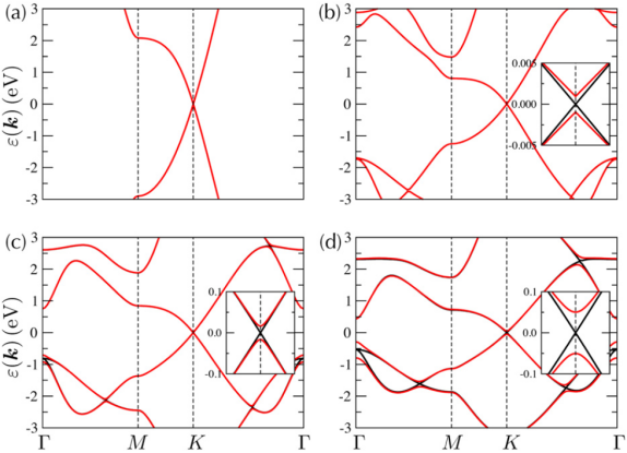
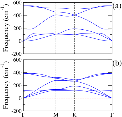
In pristine silicene the spin orbit coupling results in a band gap of 2.0 meV, see Fig. 1, which is larger than in graphene but smaller than in germanene and tinene n11 . The band gap shrinks under biaxial tensile strain udo1 . In addition, up to a strain of more than 5% the Dirac cone is located at the Fermi energy, whereas afterwards hole doping is introduced. At 10% strain, for example, the Dirac point is located 0.18 eV above the Fermi energy. Comparison of the phonon spectra of silicene without strain and under 10% strain in Fig. 2 shows that the frequencies of the G and D modes are strongly reduced. However, only at large strain above 20% the lattice becomes instable. In Ref. PRB2013 the authors have demonstrated an anomalous thermal response under uniaxial tensile strain, very different to graphene. The thermal conductivity increases monotonically, which is also true for nanoribbons, while the group velocities of the out-of-plane phonons are suppressed.
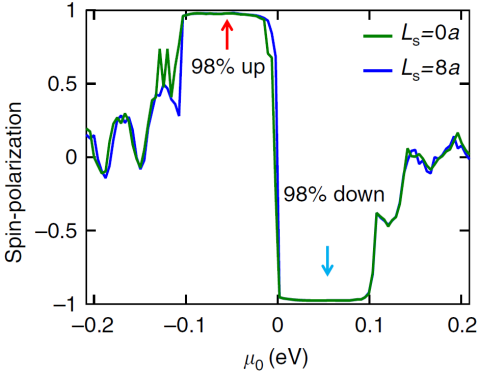
A quantum point contact of silicene has been put forward as high efficiency spin filter with quantized conductance bansil . In Fig. 3 the spin polarization is shown as a function of the effective chemical potential . For positive eV the current flows within the conduction band of the left valley with 98% spin down polarization, while for negative eV the current flows within the valence band of the right valley with 98% spin up polarization. By changing the effective chemical potential by means of a gate, the spin polarization can be reversed. The authors have also demonstrated that a transition from an indirect gap semiconductor to a zero gap state can be achieved by a Zeeman field.
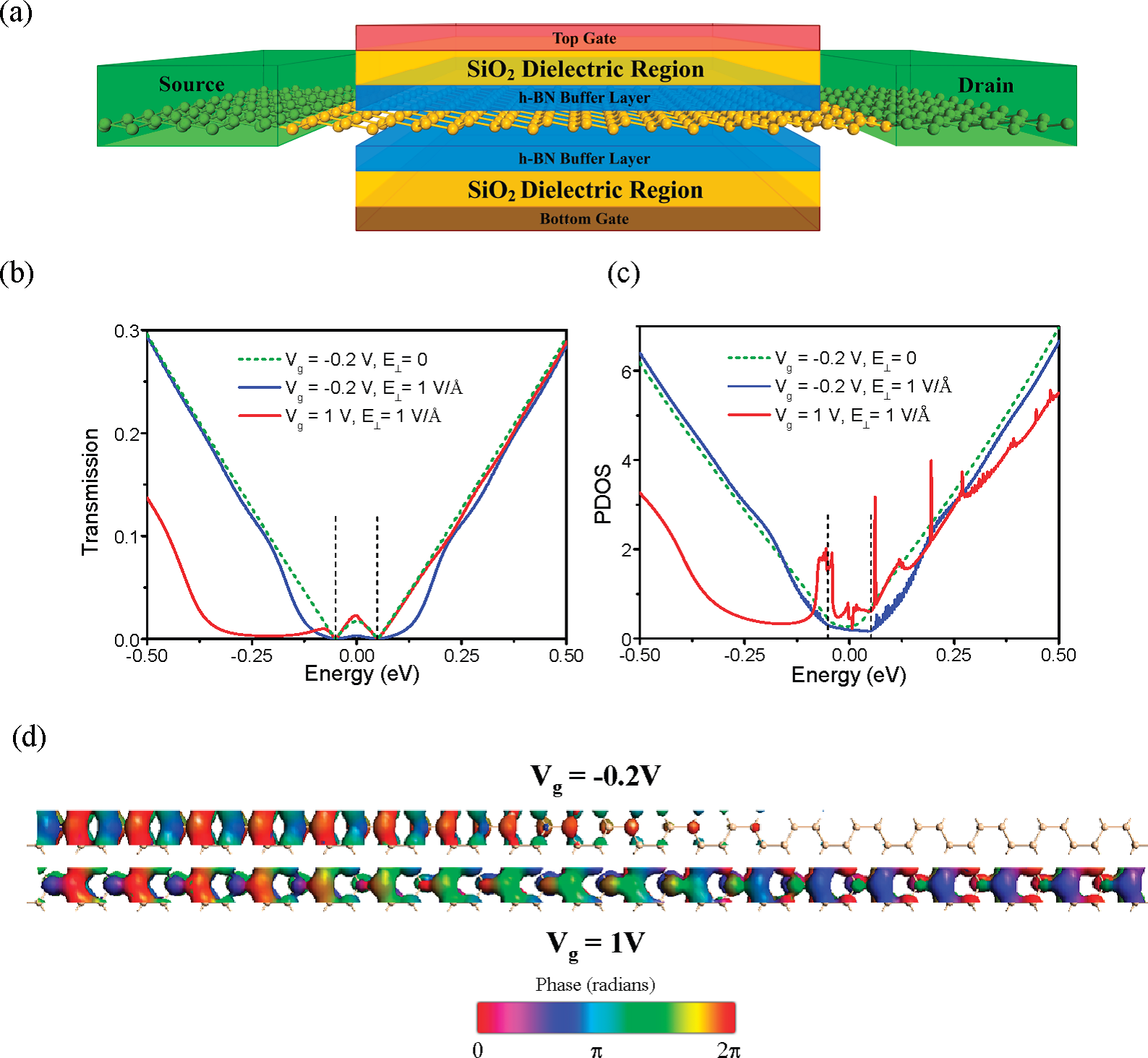
An external perpendicular electric field applied to silicene breaks the sublattice symmetry due to different onsite energies, thus opening a band gap at the K/K′-points. This is not possible in graphene, because the two sublattices lie in one plane. The variation of the band gap as a function of has been calculated in Ref. Drummond using the local density approximation and generalized gradient approximation. However, the spin orbit coupling has not been included in these calculations though it plays a key role in the vicinity of the K/K′-points. In particular, it leads to the creation of massive Dirac particles and significantly modifies the Fermi velocity n11 . Quantum transport calculations for a dual-gated silicene field effect transistor, see Fig. 4(a) for a schematic view, accordingly find under a transport gap Ni . As compared to a single-gated field effect transistor, here both the doping level and can be controlled. Since a -BN trilayer remains semiconducting upto V/Å, it can be utilized as buffer to prevent tunneling between the silicene sheet and gate. The effect of on the transmission coefficient and projected density of states is addressed in Fig. 4(b,c). A transport gap of 0.14 eV for eV indicates a strong dependence on the electric field. The transmission eigenstates are shown in Fig. 4(d). Eigenvalues of 0.09 for the OFF state and 0.87 for the ON state are obtained, reflecting a remarkable OFF/ON ratio.
The strong spin orbit coupling in silicene, as compared to graphene, combined with an external electric field can give rise to special phase transitions kaloni-sci . While we have a topologically nontrivial insulator for meV, spin splitting evolves and the band gap thus starts to shrink when is switched on. The band gap closes for meV and grows again in an almost linear manner when is further enhanced, giving rise to a band insulator. These effects could not be observed in Refs. Drummond ; Ni , because the spin orbit coupling was not taken into account.
II.2 Interaction with substrates
Silicene can be grown on Ag(111) Quaresima ; Chen ; n1 , but theory predicts that the Dirac cone will disappear prl13 . The band structure becomes complicated with the states at the Fermi energy clearly not being due to the Si orbitals. Instead, there is strong hybridization between the Si and Ag orbitals, which explains why the electronic behaviour changes fundamentally. This picture has been confirmed experimentally in Ref. afm14 . For overcoming the hybridization issue and keeping the Dirac cone intact, the interaction with the substrate has to be reduced. This can be achieved by semiconducting substrates, which are also promising for device applications similar to those already demonstrated for graphene on -BN and SiC(0001) Young1 ; Dimitrakopoulo ; Seyller ; Gannett ; Santoso ; xue ; Watanabe2 ; Zhao3 .
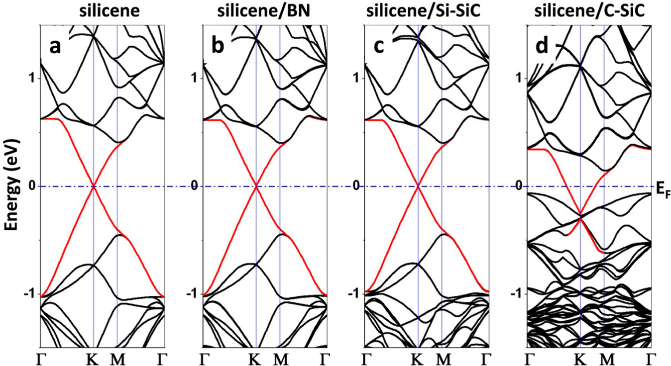
The structural and electronic properties of superlattices of silicene and -BN have been addressed in Ref. kaloni-sci . By the large band gap of -BN, it is not expected that B or N states appear in the vicinity of the Fermi energy. Indeed, a cone with a 1.6 meV band gap (as a consequence of the spin orbit coupling) is observed, which traces back to the Si orbitals and is slightly hole doped due to a small charge transfer towards the substrate. Some results for SiC(0001) and -BN substrates are summarized in Table II. It is found that silicene behaves as a free-standing sheet with a distance of 3.0 Å to the substrate. The cohesive energy is less than 90 meV per Si atom. Moreover, the Dirac point remains at the Fermi energy on H-passivated Si-SiC(0001), see Fig. 5, whereas on H-passivated C-SiC(0001) metallicity is induced by charge transfer towards the silicene sheet. This effect is understood in terms of the work function, since the valence band maximum of H-passivated C-SiC(0001) lies above that of silicene. Stability of silicene also has been predicted on Cl-passivated Si(111) as well as on CaF2(111) n4 . Interestingly, Ca-intercalation of multilayer silicene results in a Dirac cone (shifted substantially in energy due to charge transfer from the Ca atoms), which gives rise to a promising alternative from the preparation point of view n5 .
| Silicene cell | Substrate Cell | Lattice mismatch (%) | Si-Si bond length (Å) | Binding energy (meV/atom) | |
|---|---|---|---|---|---|
| silicene/-BN | 2.0 | 2.27-2.28 | 89 | ||
| silicene/Si-SiC(0001) | 0.1 | 2.27-2.28 | 67 | ||
| silicene/C-SiC(0001) | 0.1 | 2.27-2.28 | 84 |
Silicene on MoS2 substrate shows a Dirac cone with a 70 meV band gap (much larger than graphene on MoS2) and therefore is interesting for electronic devices pccp14 . In the energetically favorable structure one Si sublattice is located above S atoms and the other one above hollow sites of MoS2. The binding energy of 120 meV per Si atom is close to that of silicene on GaS (126 meV) apl13 but significantly larger than reported for -BN and SiC(0001), see Table II. The carrier density, effective mass, and mobility are hardly influenced by the presence of MoS2 Lee ; Li12 ; Hiram ; sant1 ; sant2 . Accordingly, the bands at the Fermi energy have and character. Si has been deposited on MoS2 by molecular beam epitaxial growth and the local structural and electronic properties have been investigated by scanning tunneling microscopy and spectroscopy Chiappe . The experiments show 2D domains of Si with hexagonal atomic arrangement but unexpected electronic character, which can be interpreted as a new allotropic form of Si. We note that the interaction of silicene with semiconducting substrates also can be quite substantial, e.g., metallic or magnetic states can be achieved DAS . For AlAs(111), AlP(111), and GaAs(111) the surface magnetism of the substrate is suppressed when silicene is attached, while for GaP(111) and ZnSe(111) it is enhanced.
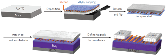
A silicene field effect transistor with room temperature mobility of about 100 cm2V-1s-1 has been demonstrated in Ref. Li-Tao . The fabrication process resulting in a silicene channel with Ag electrodes is shown in Fig. 6. After epitaxial growth of silicene on Ag(111), an Al2O3 capping layer is applied in situ, the structure is detached from the mica substrate, turned over, and transferred onto a SiO2 substrate. Then an etch-back approach is used to define the source and drain contacts in the Ag film. In the region where the Ag has been removed silicene is only in contact with semiconducting Al2O3 (weak interaction). Electrical measurements at room temperature demonstrate a transport behaviour similar to that of graphene. A linear dependence of the drain current on the drain voltage confirms an Ohmic contact. The fact that the silicene channel loses its Raman and electrical signatures while exposed to air is likely to reflect degradation to an amorphous insulator and indicates that the observed characteristics indeed are due to the silicene channel.
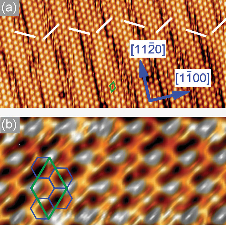
Epitaxial growth of silicene on ZrB2(0001) has been reported in Ref. Fleurence . Fig. 7(a) shows a large-scale image from scanning tunneling microscopy with domain boundaries running along the direction. The zoom in Fig. 7(b) highlights the honeycomb geometry with a lattice constant of 3.65 Å. The buckling is enhanced and loses its regularity due to strong interaction with the substrate, resulting in a large band gap of 250 meV, while the Si-Si bond length is maintained. Silicene on Ir(111) after annealing at 670 K forms a superstructure with respect to the substrate, as determined by low energy electron diffraction Meng .
II.3 Functionalization
Tuning of the band gap can be achieved by functionalization Houssa-apl ; Biberiana ; Osborn1 ; Zheng2 , similar to graphene Ramanathan1 ; Xian ; Robinson ; Shenoy ; Balakrishnan ; Wagner . Note that in this respect theoretical results obtained for free-standing silicene will also apply in the presence of a weakly interacting substrate. A sizable band gap without disturbing the electronic characteristics of silicene is particularly fruitful for field effect transistors Li-Tao . The authors of Ref. Fei have proposed that this goal is achieved by decoration with Li, Na, K, Rb, and Cs atoms (growing charge transfer along the series). The binding energy is found to decrease for increasing coverage due to dopant-dopant interaction.
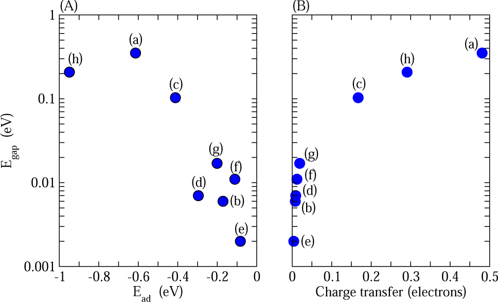
Adsorption of small organic molecules is also a very efficient way to modify the band gap freund . The molecules induce a perpendicular electric field, which breaks the sublattice symmetry and thus opens a band gap Ramasubramaniam . The adsorption energy varies from 110 meV for acetone to 905 meV for toluene, see Fig. 8(left). These values are higher than found for the adsorption of similar molecules on graphene JACS , which indicates that silicene is a good host. Band gaps between 6 meV (acetonitrile) and 350 meV (acetone) have been reported as well as mobilities even higher than in graphene, which is important for electronic devices. The charge transfer from/to the adsorbed molecule, see Fig. 8(right), is essentially proportional to the size of the band gap. The effect of H, CH3, OH, and F decoration on the electronic properties of monolayer and bilayer silicene has been studied in Ref. Denis . As compared to graphene, the bonds with Si atoms are substantially weaker, the strongest being the Si-F bond with a binding energy of 4.99 eV per atom. H and CH3 attached to monolayer silicene provide optical band gaps of 3.2 eV, while OH and F result in metallicity. F also strongly modifies the electronic structure of bilayer silicene and yields a large band gap of 3.0 eV, whereas for the other adsorbants band gaps between 0.1 eV and 0.6 eV are found.
A rich phase diagram of silicene (and analogously of germanene) in the presence of exchange and perpendicular electric fields results already from a simplified model Hamiltonian, comprising quantum spin Hall, quantum anomalous Hall, band insulating, and valley-polarized metallic phases ezawa . The quantum spin Hall state has been confirmed by calculating the topological invariant from the first principles electronic band structure of silicene n6 and by a tight-binding approach for germanene nanoribbons n7 . A quantum anomalous Hall state has been described theoretically for Co-decorated silicene kaloni-prb , while for other transition metals (Ti, V, Cr, Mn, and Fe) the state is prohibited by pertubations of the Dirac cone. In addition, it has been demonstrated that only for a sufficiently low Co coverage the quantum anomalous Hall state is realized. For larger Co coverage the Co-Co interaction modifies the shape of the electronic bands strongly in the vicinity of the Fermi energy. In contrast to Ref. kaloni-prb , topologically non-trivial states have been predicted for V-decorated silicene in Ref. Zhang-sci , but only if an onsite Coulomb interaction is taken into account. The quantum anomalous Hall state is prohibited in the case of Ti, Cr, and Mn decoration by hybridization between the Si and transition metal states.
III Germanene
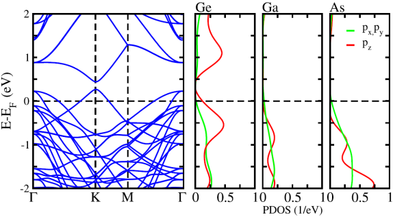
Semiconducting GaAs(0001) interacts strongly with germanene, forming bonds with a binding energy of 568 meV per Ge atom, while on H-passivated GaAs(0001) the interaction is reduced to 69 meV per Ge atom kaloni-jap . This value comes close to the experimental binding energy of graphene sheets in graphite Ulbricht . According to Fig. 9, the electronic bands are forming hole pockets at the -point (due to Ga and As states), while a split Dirac cone (energy gap of 175 meV, as a consequence of the broken sublattice symmetry) appears above the Fermi energy. Application of an appropriate voltage can bring it back to the Fermi energy to induce a semiconducting state.
It has been shown that germanene can be grown on Au(111) with a binding energy of 110 meV per Ge atom NJP . Since this value is lower than the binding energy in bulk Ge, formation of Ge clusters is to be expected. Moreover, ab-initio simulations point to a honeycomb lattice with weak corrugations. Single phase growth of germanene has been reported on Al(111) nano-2015 . The energetics and electronic structure suggest that graphene also can be used as substrate PRB-germanene . The interaction is weak and a band gap of 57 meV is realized, which is more than twice that of the pristine material (24 meV). Germanene on ZnSe(0001) shows an indirect band gap of 400 meV, whereas a charge transfer analysis points to only weak interaction ass . An electric field of V/Å results in transition to a direct band gap.
Concerning metallic substrates, germanene has been claimed to be achieved on Pt(111) by deposition of Ge atoms with subsequent annealing Li ; Bampoulis . Low energy electron diffraction and scanning tunneling microscopy measurements have been interpreted in terms of commensurability with a pattern. These findings have been disputed by vec and co-workers, who rule out the formation of silicene or germanene on transition metal surfaces Hapala . Based on various experimental and theoretical techniques, their comprehensive study instead points to the formation of an ordered 2D surface alloy. On the other hand, deposition of Pt on Ge(110) followed by annealing at 1100 K results in three-dimensional Pt-Ge nanocrystals Bampoulis . Interestingly, the outermost layer of these crystals possesses a honeycomb structure, consisting of two hexagonal sublattices displaced by about 0.2 Å with respect to each other. The nearest neighbor distance of 2.5 Å agrees well with the Ge-Ge bond length in pristine germanene.
Alkali metal atoms are found to be strongly bound on germanene and capable of engineering a band gap of 20 meV to 310 meV physicae . The observed large carrier mobility has been put forward for high speed field effect transistors. The structural and electronic properties induced by alkali, alkaline-earth, group-III, and transition metal atoms adsorbed on germanene have been studied in Ref. pccp-14 . Alkali metals (Li, Na, and K) become ionized and lead to metallicity, while alkali-earth metals (Be, Mg, and Ca) result in a mixed ionic/covalent bonding and a semiconducting state. For group-III atoms (Al, Ga, and In) the interaction is enhanced (mixed ionic/covalent bonding) and transition metals (Ti, V, Cr, Fe, Co, and Ni) finally result in large distortions of the germanene sheet, where metallic, half-metallic, and semiconducting states can be realized. The effect of Mn decoration has been investigated in Ref. kaloni-jpcc as a function of the coverage.
IV Summary
Substantial progress has been achieved towards applications of silicene and germanene. Silicene nowadays can be grown on different Ag surfaces, Ir(111), MoS2, and ZrB2(0001). Energetical stability also has been predicted on -BN, H-passivated C-SiC(0001) and Si-SiC(0001), Cl-passivated Si(111), CaF2, AlAs(111), AlP(111), GaAs(111), GaP(111), ZnSe(111), and ZnS(111). Particularly the semiconducting substrates are of technological interest, because the interaction with silicene is reduced and the Dirac states consequently are maintained, even though a sizable band gap may develop. In the cases of -BN and H-passivated Si-SiC(0001) the effects of the interaction are close to negligible so that quasi-free-standing silicene may be realized. Band gap control is achieved by external electric fields and decoration with alkali, alkali-earth, and transition metal atoms. According to theoretical predictions, the decoration approach furthermore provides access to a multitude of exotic phases. Germanene has been grown on Al(111) and Au(111), and the possibility of growth on GaAs(0001), graphene, and ZnSe(0001) has been put forward. Again the band gap is susceptible to engineering approaches based on atomic decoration.
Acknowledgements.
Research reported in this publication was supported by the King Abdullah University of Science and Technology (KAUST). G.S. acknowledges funding from the Natural Sciences and Engineering Council of Canada (NSERC, Discovery Grant). M.S.F. acknowledges support by the Natural Sciences and Engineering Research Council (NSERC) of Canada, the Canada Research Chair program, Canada Foundation for Innovation (CFI), the Manitoba Research and Innovation Fund, and the University of Manitoba.References
- (1) K. S. Novoselov, A. K. Geim, S. Morozov, D. Jiang, Y. Zhang, S. V. Dubonos, I. V. Grigorieva, and A. A. Firsov, Science 306, 666 (2004).
- (2) M. Xu, T. Liang, M. Shi, and H. Chen, Chem. Rev. 113, 3766 (2013).
- (3) K. Watanabe, T. Taniguchi, and H. Kanda, Nat. Mater. 3, 404 (2004).
- (4) Y. Kubota, K. Watanabe, O. Tsuda, and T. Taniguchi, Science 317, 932 (2007).
- (5) D. Pacilé, J. C. Meyer, Ç. Ö. Girit, and A. Zettl, Appl. Phys. Lett. 92, 133107 (2008).
- (6) K. S. Novoselov, V. I. Fal ko, L. Colombo, P. R. Gellert, M. G. Schwab, and K. Kim, Nature 490, 192 (2012).
- (7) A. K. Geim, Nature 499, 419 (2013).
- (8) K. C. Santosh, R. L. Pazos, R. Addou, R. Wallace, and K. Cho, Nanotechnology 25, 375703 (2014).
- (9) A. Azcatl, S. McDonnell, K. C. Santosh, X. Peng, H. Dong, X. Qin, R. Addou, G. Mordi, N. Lu, J. Kim, M. J. Kim, K. Cho, and R. M. Wallace, Appl. Phys. Lett. 104, 111601 (2014).
- (10) S. Cahangirov, M. Topsakal, E. Aktürk, H. Şahin, and S. Ciraci, Phys. Rev. Lett. 102, 236804 (2012).
- (11) A. Fleurence, R. Friedlein, T. Ozaki, H. Kawai, Y. Wang, and Y. Yamada-Takamura, Phys. Rev. Lett. 108, 245501 (2012).
- (12) P. Vogt, P. D. Padova, C. Quaresima, J. Avila, E. Frantzeskakis, M. C. Asensio, A. Resta, B. Ealet, and G. L. Lay, Phys. Rev. Lett. 108, 155501 (2012).
- (13) L. Chen, C.-C. Liu, B. Feng, X. He, P. Cheng, Z. Ding, S. Meng, Y. Yao, and K. Wu, Phys. Rev. Lett. 109, 056804 (2012).
- (14) L. Meng, Y. Wang, L. Zhang, S. Du, R. Wu, L. Li, Y. Zhang, G. Li, H. Zhou, W. A. Hofer, and H.-J. Gao, Nano Lett. 13, 685 (2013).
- (15) D. Jose and A. Datta, Acc. Chem. Res. 47, 593 (2014).
- (16) T. P. Kaloni and U. Schwingenschlögl, J. Appl. Phys. 114, 184307 (2013).
- (17) L. Lia and M. Zhao, Phys. Chem. Chem. Phys. 15, 16853 (2013).
- (18) M. E. Dávila, L. Xian, S. Cahangirov, A. Rubio, and G. Le Lay, New J. Phys. 16, 095002 (2014).
- (19) M. Derivaz, D. Dentel, R. Stephan, M.-C. Hanf, A. Mehdaoui, P. Sonnet, and C. Pirri, Nano Lett. 15, 2510 (2015).
- (20) V. O. Özçelik, S. Cahangirov, and S. Ciraci, Phys. Rev. Lett. 112, 246803 (2014).
- (21) K. Takeda and K. Shiraishi, Phys. Rev. B 50, 14916 (1994).
- (22) G. G. Guzmán-Verri and L. C. L. Y. Voon, Phys. Rev. B 76, 075131 (2007).
- (23) S. S. Cahangirov, M. Topsakal, E. Aktürk, H. Şahin, and S. Ciraci, Phys. Rev. Lett. 102, 236804 (2009).
- (24) W. Ke-Hui, Chin. Phys. B 24, 086802 (2015).
- (25) C.-L. Lin, R. Arafune, K. Kawahara, M. Kanno, N. Tsukahara, E. Minamitani, Y. Kim, M. Kawai, and N. Takagi, Phys. Rev. Lett. 110, 076801 (2013).
- (26) S. Cahangirov, M. Audiffred, P. Tang, A. Iacomino, W. Duan, G. Merino, and A. Rubio, Phys. Rev. B 88, 035432 (2013).
- (27) Y.-P. Wang, and H.-P. Cheng, Phys. Rev. B 87, 245430 (2013).
- (28) T. P. Kaloni, M. Tahir, and U. Schwingenschlögl, Sci. Rep. 3, 3192 (2013).
- (29) H. Liu, J. Gao, and J. Zhao, J. Phys. Chem. C 117, 10353 (2013).
- (30) R. Quhe, Y. Yuan, J. Zheng, Y. Wang, Z. Ni, J. Shi, D. Yu, J. Yang, and J. Lu, Sci. Rep. 4, 5476 (2014).
- (31) S. Lebegue and O. Eriksson, Phys. Rev. B 79, 115409 (2009).
- (32) G. Liu, M. S. Wu, C. Y. Ouyang, and B. Xu, EPL 99, 17010 (2012).
- (33) L. Matthes, O. Pulci, and F. Bechstedt, J. Phys.: Condens. Matter 25, 395305 (2013).
- (34) T. P. Kaloni, Y. C. Cheng, and U. Schwingenschlögl, J. Appl. Phys. 113, 104305 (2013).
- (35) B. Wang, J. Wu, X. Gu, H. Yin, Y. Wei, R. Yang, and M. Dresselhaus, Appl. Phys. Lett. 104, 081902 (2014).
- (36) N. D. Drummond, V. Zólyomi, and V. I. Fal’ko, Phys. Rev. B 85, 075423 (2012).
- (37) Z. Ni, Q. Liu, K. Tang, J. Zheng, J. Zhou, R. Qin, Z. Gao, D. Yu, and J. Lu, Nano Lett. 12, 113 (2012).
- (38) M. Ezawa, Phys. Rev. B 86, 161407 (2012).
- (39) H. H. Gürel, V. O. Özcelik, and S. Ciraci, J. Phys.: Condens. Matter 25, 305007 (2013).
- (40) Y.-C. Zhao and J. Ni, Phys. Chem. Chem. Phys. 16, 15477 (2014).
- (41) M. Houssa, E. Scalise, K. Sankaran, G. Pourtois, V. V. Afanasev, and A. Stesmans, Appl. Phys. Lett. 98, 223107 (2011).
- (42) W. Wei and T. Jacob, Phys. Rev. B 88, 045203 (2013).
- (43) T. Hussain, T. Kaewmaraya, S. Chakraborty, and R. Ahuja, Phys. Chem. Chem. Phys. 21, 18900 (2013).
- (44) G. Liu, X. L. Lei, M. S. Wu, B. Xu, and C. Y. Ouyang, EPL 106, 47001 (2014).
- (45) T. P. Kaloni, G. Schreckenbach, and M. S. Freund, J. Phys. Chem. C 118, 23361 (2014).
- (46) R. Quhe, R. Fei, Q. Liu, J. Zheng, H. Li, C. Xu, Z. Ni, Y. Wang, D. Yu, Z. Gao, and J. Lu, Sci. Rep. 2, 853 (2012).
- (47) T. P. Kaloni and U. Schwingenschlögl, Phys. Status Solidi RRL 8, 685 (2014).
- (48) X. Lin and J. Ni, Phys. Rev. B 86, 075440 (2012).
- (49) J. Zhang, B. Zhao, and Z. Yang, Phys. Rev. B 88, 165422 (2013).
- (50) X.-L. Zhang, L.-F. Liu, and W.-M. Liu, Sci. Rep. 3, 2908 (2013).
- (51) T. P. Kaloni, N. Singh, and U. Schwingenschlögl, Phys. Rev. B 89, 035409 (2014).
- (52) L. Matthes, P. Gori, O. Pulci, and F. Bechstedt, Phys. Rev. B 87, 035438 (2013).
- (53) W. Wei, Y. Dai, B. Huang, and T. Jacob, Phys. Chem. Chem. Phys. 15, 8789 (2013).
- (54) O. Pulci, P. Gori, M. Marsili, V. Garbuio, R. Del Sole, and F. Bechstedt, EPL 98, 37004 (2012).
- (55) Y. Cai, C.-P. Chuu, C. M. Wei, and M. Y. Chou, Phys. Rev. B 88, 245408 (2013).
- (56) T. P. Kaloni and U. Schwingenschlögl, Chem. Phys. Lett. 583, 137 (2013).
- (57) J.-A. Yan, R. Stein, D. M. Schaefer, X.-Q. Wang, and M. Y. Chou, Phys. Rev. B 88, 121403 (2013)
- (58) N. J. Roome and J. D. Carey, ACS Appl. Mater. Interfaces 6, 7743 (2014).
- (59) Y. Ma , Y. Dai, C. Niu, and B. Huang, J. Mater. Chem. 22, 12587 (2012).
- (60) A. O’Hare, F. V. Kusmartsev, and K. I. Kugel, Nano Lett. 12, 1045 (2012).
- (61) Y. Li and Z. Chen, J. Phys. Chem. C 118, 1148 (2014)
- (62) C. Si, J. Liu, Y. Xu, J. Wu, B.-L. Gu, and W. Duan, Phys. Rev. B 89, 115429 (2014).
- (63) T. P. Kaloni, J. Phys. Chem. C 118, 25200 (2014).
- (64) S.-S. Li, C.-W. Zhang, W.-X. Ji, F. Li, P.-J. Wang, S.-J. Hu, S.-S. Yan, and Y.-S. Liu, Phys. Chem. Chem. Phys. 10.1039/C4CP01211A.
- (65) Y. Ma, Y. Dai, C. Niua, and B. Huanga, J. Mater. Chem. 22, 12587 (2012).
- (66) L. Seixas, J. E. Padilha, and A. Fazzio, Phys. Rev. B 89, 195403 (2014).
- (67) S.-M. Huang, S.-T. Lee, and C.-Y. Mou, Phys. Rev. B 89, 195444 (2014).
- (68) C. J. Tabert and E. J. Nicol, Phys. Rev. B 87, 235426 (2013).
- (69) S. Rachel and M. Ezawa, Phys. Rev. B 89, 195303 (2014).
- (70) K. Yang, S. Cahangirov, A. Cantarero, A. Rubio, and R. D’Agosta, Phys. Rev. B 89, 125403 (2014).
- (71) L. Li and M. Zhao, Phys. Chem. Chem. Phys. 15, 16853 (2013).
- (72) E. Bianco, S. Butler, S. Jiang, O. D. Restrepo, W. Windl, and J. E. Goldberger, ACS Nano 7, 4414 (2013).
- (73) S. Cahangirov, V. O. Özcelik, L. Xian, J. Avila, S. Cho, M. C. Asensio, S. Ciraci, and A. Rubio, Phys. Rev. B 90, 035448 (2014).
- (74) F. Matusalem, M. Marques, L. K. Teles, and F. Bechstedt, Phys. Rev. B 92, 045436 (2015).
- (75) X.-L. Wang, S. X. Dou, and C. Zhang, NPG Asia Materials 2, 31 (2010).
- (76) H. Sahin and F. M. Peeters, Phys. Rev. B 87, 085423 (2013).
- (77) A. H. Castro Neto, F. Guinea, N. M. R. Peres, K. S. Novoselov, and A. K. Geim, Rev. Mod. Phys. 81, 109 (2009).
- (78) T. O. Wehling, E. Şaşıoğlu, C. Friedrich, A. I. Lichtenstein, M. I. Katsnelson, and S. Blügel, Phys. Rev. Lett. 106, 236805 (2011).
- (79) E. Scalise, M. Houssa, G. Pourtois, B. van den Broek, V. Afanasev, and A. Stesmans, Nano Res. 6, 19 (2013).
- (80) P. Koskinen, S. Malola, and H. Häkkinen, Phys. Rev. Lett. 101, 115502 (2008).
- (81) H. Shin, S. Kang, J. Koo, H. Lee, J. Kim, and Y. Kwon, J. Chem. Phys. 140, 114702 (2014).
- (82) C.-C. Liu, H. Jiang, and Y. Yao, Phys. Rev. B 84, 195430 (2011).
- (83) M. Hu, X. Zhang, and D. Poulikakos, Phys. Rev. B 87, 195417 (2013).
- (84) W.-F. Tsai, C.-Y. Huang, T.-R. Chang, H. Lin, H.-T. Jeng, and A. Bansil, Nat. Commun. 4, 1500 (2013).
- (85) C.-L. Lin, R. Arafune, K. Kawahara, M. Kanno, N. Tsukahara, E. Minamitani, Y. Kim, M. Kawai, and N. Takagi, Phys. Rev. Lett. 110, 076801 (2013).
- (86) N. W. Johnson, P. Vogt, A. Resta P. D. Padova, I. Perez, D. Muir, E. Z. Kurmaev, G. Le Lay, and A. Moewes, Adv. Funct. Mater. 24, 5253 (2014).
- (87) C. R. Dean, A. F. Young, I. Meric, C. Lee, L. Wang, S. Sorgenfrei, K. Watanabe, T. Taniguchi, P. Kim, K. L. Shepard, and J. Hone, Nat. Nanotechnol. 5, 722 (2010).
- (88) Y.-M. Lin, C. Dimitrakopoulos, K. A. Jenkins, D. B. Farmer, H.-Y. Chiu, A. Grill, and P. Avouris, Science 327, 662 (2010).
- (89) P. N. First, W. A. de Heer, T. Seyller, C. Berger, J. A. Stroscio, and J.-S. Moon, MRS Bull. 35, 296 (2010).
- (90) W. Gannett, W. Regan, K. Watanabe, T. Taniguchi, M. F. Crommie, and A. Zettl, Appl. Phys. Lett. 98, 242105 (2011).
- (91) S. L. Wong, H. Huang, Y. Wang, L. Cao, D. Qi, I. Santoso, W. Chen, and A. T. S. Wee, ACS Nano 5, 7662 (2011).
- (92) J. Xue, J. Sanchez-Yamagishi, D. Bulmash, P. Jacquod, A. Deshpande, K. Watanabe, T. Taniguchi, P. Jarillo-Herrero, and B. J. LeRoy, Nat. Mater. 10, 282 (2011).
- (93) M. Yankowitz, J. Xue, D. Cormode, J. D. Sanchez-Yamagishi, K. Watanabe, T. Taniguchi, P. Jarillo-Herrero, P. Jacquod, and B. J. LeRoy, Nat. Phys. 8, 382 (2012).
- (94) H. Liu, J. Gao, and J. Zhao, J. Phys.: Conf. Ser. 491, 012007 (2014).
- (95) S. Kokott, P. Pflugradt, L. Matthes, and F. Bechstedt, J. Phys.: Condens. Matter 26, 185002 (2014).
- (96) E. Noguchi, K. Sugawara, R. Yaokawa, T. Hitosugi, H. Nakano, and T. Takahashi, Adv. Mater. 27, 856 (2015).
- (97) N. Gao, J. C. Li, and Q. Jiang, Phys. Chem. Chem. Phys. 16, 11673 (2014).
- (98) Y. Ding and Y. Wang, Appl. Phys. Lett. 103, 043114 (2013).
- (99) K. F. Mak, C. Lee, J. Hone, J. Shan, and T. F. Heinz, Phys. Rev. Lett. 105, 136805 (2010).
- (100) Y. Li and Z. Chen, J. Phys. Chem. Lett. 4, 269 (2012).
- (101) J. H. Conley, B. Wang, J. I. Ziegler, R. F. Haglund, S. T. Pantelides, and K. I. Bolotin, Nano Lett. 13, 3626 (2013).
- (102) D. Chiappe, E. Scalise, E. Cinquanta, C. Grazianetti, B. van den Broek, M. Fanciulli, M. Houssa, and A. Molle, Adv. Mater. 26, 2096 (2014).
- (103) A. Bhattacharya, S. Bhattacharya, and G. P. Das, Appl. Phys. Lett. 103, 123113 (2013).
- (104) L. Tao, E. Cinquanta, D. Chiappe, C. Grazianetti, M. Fanciulli, M. Dubey, A. Molle, and D. Akinwande, Nat. Nanotechnol. 10, 227 (2015).
- (105) G. Le Lay, B. Aufray, C. Léandri, H. Oughaddou, J.-P. Biberian, P. D. Padova, M.E. Dávila, B. Ealet, and A. Kara, Appl. Surf. Sci. 256, 524 (2009).
- (106) T. H. Osborn, A. A. Farajian, O. V. Pupysheva, R. S. Aga, and L. C. L. Y. Voon, Chem. Phys. Lett. 511, 101 (2011).
- (107) N. Gao, W. T. Zheng, and Q. Jiang, Phys. Chem. Chem. Phys. 14, 257 (2012)
- (108) T. Ramanathan, A. A. Abdala, S. Stankovich, D. A. Dikin, M. Herrera-Alonso, R. D. Piner, D. H. Adamson, H. C. Schniepp, X. Chen, R. S. Ruoff, S. T. Nguyen, I. A. Aksay, R. K. Prud’Homme, and L. C. Brinson, Nat. Nanotechnol. 3, 327 (2008).
- (109) J.-A. Yan, L. Xian, and M. Y. Chou, Phys. Rev. Lett. 103, 086802 (2009).
- (110) J. T. Robinson, J. S. Burgess, C. E. Junkermeier, S. C. Badescu, T. L. Reinecke, F. K. Perkins, Maxim K. Zalalutdniov, J. W. Baldwin, J. C. Culbertson, P. E. Sheehan, and E. S. Snow, Nano Lett. 10, 3001 (2010).
- (111) A. Bagri, C. Mattevi, M. Acik, Y. J. Chabal, M. Chhowalla, and V. B. Shenoy, Nat. Chem. 2, 581 (2010).
- (112) J. Balakrishnan, G. K. W. Koon, M. Jaiswal, A. H. Castro Neto, and B. Özyilmaz, Nat. Phys. 9, 284 (2013).
- (113) P. Wagner, V. V. Ivanovskaya, M. Melle-Franco, B. Humbert, J.-J. Adjizian, P. R. Briddon, and C. P. Ewels, Phys. Rev. B 88, 094106 (2013).
- (114) A. Ramasubramaniam, D. Naveh, and E. Towe, Nano Lett. 11, 1070 (2011).
- (115) P. Lazar, F. Karlický, P. Jurecka, K. Kocman, E. Otyepková, K. Safároá, M. Otyepka, J. Am. Chem. Soc. 135, 6372 (2013).
- (116) P. A. Denis, Phys. Chem. Chem. Phys., DOI: 10.1039/C4CP05331A.
- (117) M. Ezawa, Phys. Rev. Lett. 109, 055502 (2012).
- (118) C.-C. Liu, W. Feng, and Y. Yao, Phys. Rev. Lett. 107, 076802 (2011).
- (119) L. Matthes and F. Bechstedt, Phys. Rev. B 90, 165431 (2014).
- (120) T. P. Kaloni, S. Gangopadhyay, N. Singh, B. Jones, and U. Schwingenschlögl, Phys. Rev. B 88, 235418 (2013).
- (121) R. Zacharia, H. Ulbricht, and T. Hertel, Phys. Rev. B 69, 155406 (2004).
- (122) Y. Cai, C.-P. Chuu, C. M. Wei, and M. Y. Chou, Phys. Rev. B 88, 245408 (2013).
- (123) M. Houssa, B. van den Broek, E. Scalise, B. Ealet, G. Pourtois, D. Chiappe, E. Cinquanta, C. Grazianetti, M. Fanciulli, A. Molle, V. V. Afanasev, and A. Stesmans, Appl. Sur. Sci. 291, 98 (2014).
- (124) L. Li, S.-Z. Lu, J. Pan, Z. Qin, Y.-Q. Wang, Y. Wang, G.-Y. Cao, S. Du, and H.-J. Gao, Adv. Mater. 26, 4820 (2014).
- (125) P. Bampoulis, L. Zhang, A. Safaei, R. V. Gastel, B. Poelsema, and H. J. W. Zandvliet, J. Phys.: Condens. Matter 26, 442001 (2014).
- (126) M. vec, P. Hapala, M. Ondráek, P. Merino, M. Blanco-Rey, P. Mutombo, M. Vondráek, Y. Polyak, V. Cháb, J. A. Martín Gago, and P. Jelínek, Phys. Rev. B 89, 201412 (2014).
- (127) M. Ye, R. Quhe, J. Zheng, Z. Ni, Y. Wang, Y. Yuan, G. Tse, J. Shi, Z. Gao, and J. Lu, Physica E 59, 60 (2014).
- (128) S.-S. Li, C.-W. Zhang, W.-X. Ji, F. Li, P.-J. Wang, S.-J. Hu, S.-S. Yan, and Y.-S. Liu, Phys. Chem. Chem. Phys. 16, 15968 (2014).