Chiral and Non-Chiral Edge States in Quantum Hall Systems
with Charge Density Modulation
Abstract
We consider a system of weakly coupled wires with quantum Hall effect (QHE) and in the presence of a spatially periodic modulation of the chemical potential along the wire, equivalent to a charge density wave (CDW). We investigate the competition between the two effects which both open a gap. We show that by changing the ratio between the amplitudes of the CDW modulation and the tunneling between wires, one can switch between non-topological CDW-dominated phase to topological QHE-dominated phase. Both phases host edge states of chiral and non-chiral nature robust to on-site disorder. However, only in the topological phase, the edge states are immune to disorder in the phase shifts of the CDWs. We provide analytical solutions for filling factor and study numerically effects of disorder as well as present numerical results for higher filling factors.
pacs:
71.10.Fd; 73.43.-f; 71.10.PmIntroduction. Over the last decades topological states of matter attracted a lot of attention both theoretically and experimentally. The striking stability of the quantum Hall effect (QHE) Klitzing et al. (1980); Tsui et al. (1982) can be linked to topology Thouless et al. (1982). The time-reversal invariant cousins of the QHE are the two-dimensional (2D) topological insulators (TIs) for which many candidate materials were found or synthesized in recent years Hasan and Kane (2010). However, despite great progress, the conductance quantization in TI materials is still not as perfect as in the QHE. Thus, the experimental focus has shifted in recent years to a more direct study of the edge state physics in TIs, for instance via Fraunhofer patterns Hart et al. (2014); Pribiag et al. (2015) and SQUID probes Spanton et al. (2014); Wang et al. (2015). However, the edge states, especially in clean samples, could also be of non-topological origin, for example, due to Tamm-Shockley states Tamm (1932); Shockley (1939); Gangadharaiah et al. (2012).
Recently, edge state behavior was observed in 2D GaSb heterostructures, but in a regime that is believed to be non-topological, and thus challenging the standard interpretation of this system as a TI Nichele et al. (2015). The origin of this unexpected observation is still unclear but it raises the intriguing question whether edge states could not occur in both phases, in the topological as well as in the trivial one, but with different signatures such as e.g. being helical (chiral) in one phase vs. non-helical (non-chiral) in the other. In other words, the system could host topological edge states for one set of parameters while there exist non-topological edge states for an other one. It is thus of fundamental interest to see if realistic models can be constructed which demonstrate that, in principle, these two scenarios do not need to exclude each other.
In the present work, we propose a system related to the QHE regime where exactly such a mixed behavior of edge state physics can emerge. The system we consider is given by a 2D array of tunnel coupled wires in the presence of a magnetic field and charge density waves (CDWs) inside the wires. This provides two different mechanisms (QHE and CDW) for inducing gaps and edge states which can compete with each other. Such CDWs may be induced intrinsically by electron-electron interactions Giamarchi (2003); Klinovaja and Loss (2014); Bedell (1994), extrinsically by periodically arranged gates inducing spatial modulations of the chemical potential, or by an internal superlattice structure Algra et al. (2008); Deutschmann et al. (2001), see Fig. 1. We show that by tuning the ratio between the amplitude of the CDW modulation and the tunneling amplitude between the wires the system undergoes a phase transition between a non-topological (CDW dominated) phase, which supports predominantly non-chiral edge states, and a topological (QHE dominated) phase, which supports predominantly chiral edge states. However, in both phases, one can find both chiral and non-chiral regimes. These results are supported by both numerical and analytical calculations. We confirm numerically that, as expected, the topological chiral states are less susceptible to disorder.
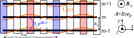
Tight-binding model. We consider a 2D coupled wire construction Lebed (1986); Yakovenko (1991); Klinovaja and Loss (2013a); Teo and Kane (2014); Klinovaja and Tserkovnyak (2014); Seroussi et al. (2014); Sagi and Oreg (2014); Meng and Sela (2014); Klinovaja et al. (2015); Meng et al. (2015) in the presence of a perpendicular uniform magnetic field, see Fig. 1. We assume that the propagation is anisotropic in the plane, mainly for analytical convenience. The tunneling amplitude along the wires, aligned in the direction, is thus larger than the one between the wires in the direction. This allows us to treat the wires as independent one-dimensional channels only weakly coupled to their neighboring wires. In addition, we include a CDW modulation along the wire. The system is then described by the following tight-binding Hamiltonian,
| (1) | |||
where is the annihilation operator acting on the electron at a site of the lattice with the lattice constant () in the () direction. For simplicity we consider spinless electrons in this work. We choose the hopping amplitude along the direction to be much larger than the hopping along the direction . The uniform magnetic field applied in the direction, , and the corresponding vector potential is chosen along the axis, yielding the orbital Peierls phase . The chemical potential is modulated with the CDW amplitude and the period . The angle is the phase of the CDW at the left edge of the wire ().
With this choice of the vector potential , the system is translation invariant in the direction, thus, we can introduce the momentum via Fourier transformation , where is the number of lattice sites in the direction. The Hamiltonian becomes diagonal in space,
| (2) | |||
As a result, the eigenfunctions of factorize as , with , . From now on, we focus on and treat as a parameter.
Continuum model. To obtain the analytical solution, it is convenient to change to the continuum description Braunecker et al. (2010); Klinovaja and Loss (2012). In this case, the resonant magnetic field leading to , corresponds to the filling factor Klinovaja and Loss (2013a). In the weak tunneling and weak modulation regime, the spectrum can be linearized around the Fermi points, , defined via the chemical potential as . In the regime of interest, the CDW modulation competes with the quantum Hall effect when the period of the CDW is chosen to be resonant, i.e., . The electron operators can be expressed in terms of slowly varying right and left movers as . The corresponding Hamiltonian density , defined via , can be written in terms of Pauli matrices acting on the left-right mover subspace as
| (3) |
where is the momentum operator and the Fermi velocity is given by . The bulk energy spectrum is given by
| (4) |
and depends on both and momenta. Here, () corresponds to the part of the spectrum above (below) . The size of the bulk gap for given becomes
| (5) |
We note that the system is gapless if and but fully gapped otherwise, see Fig. 2. This closing and reopening of the gap hints to a topological phase transition Alicea (2012). For a strip of width , one can thus expect the presence of edge states at the boundaries with energies lying inside the bulk gap. In order to explore the possibility of such edge states we consider a semi-infinite strip () and exploit the method developed in Ref. Klinovaja et al., 2012. Furthermore we assume that is much larger than the localization length of the edge state Rainis et al. (2013). Thus, we impose vanishing boundary conditions at the end of the strip , which further imposes the constraint . The energy spectrum of the edge state is then found to be
| (6) |
under the condition that . The corresponding wavefunction of the left edge state at energy is given by with the localization length
| (7) |
These edge states propagate along the boundaries in direction. They can be considered as 1D extension of fractional fermions of the Jackiw-Rebbi type Gangadharaiah et al. (2012); Jackiw and Rebbi (1976); Su et al. (1979); Kivelson and Schrieffer (1982); Klinovaja et al. (2012); Klinovaja and Loss (2013b).
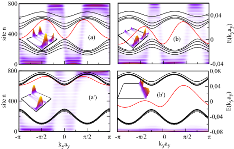
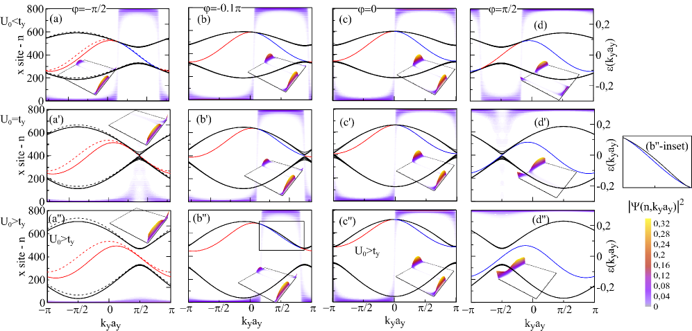
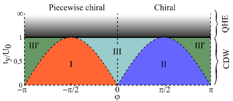
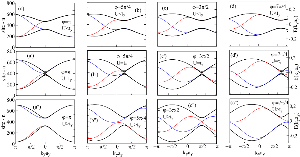
Topological transition between CDW and QHE phase. There are two important phases the system can be tuned into: The non-topological phase, dominated by the CDW modulation, and the topological QHE phase at filling factor (higher filling factors are discussed in the Appendix. B), dominated by the magnetic field. We study now the transition between these two phases both analytically and by diagonalizing numerically the tight-binding Hamiltonians, see Eqs. (Chiral and Non-Chiral Edge States in Quantum Hall Systems with Charge Density Modulation) and (Chiral and Non-Chiral Edge States in Quantum Hall Systems with Charge Density Modulation). In the calculations we fix the parameters as follows: and . The topological transition is induced by changing the amplitude of the CDW with respect to the tunneling amplitude between wires. We are interested in the bulk band represented by the edge of the gap and in the edge state wave function probability and its dispersion .
In the topological phase, , the edge state spectrum merges with the bulk gap at two points (one from the electron band and one from the hole band) determined by the condition , leading to . In other words, for any given value of , the edge state exists only for the range of momenta , see Fig. 2(a)-(d). Here, we can further distinguish between two regimes. If [] corresponding to the chiral (piecewise chiral) regime, the sign of the Fermi velocity is independent of (depends on) , as illustrated in Fig. 2(a) by the dispersion of the right (chiral) and left (piecewise chiral) edge state. In the piecewise chiral regime, there is a range of , for which the edge states are non-chiral, i.e., there are two counterpropagating edge modes at a given boundary in contrast to the single edge mode in the chiral regime, where the velocities are opposite at opposite boundaries. In the topological phase, a non-chiral behaviour is observed for inside the bulk gap. One can also notice the asymmetry in the localization length between the right and left edge states. For example, if , see Fig. 2(a) [, see Fig. 2(d)], the left (right) edge state is more strongly localized than the opposite one which is consistent with Eq. (7) and the 2D finite size calculations [see Fig. 4 (b)] even in the presence of disorder [see Figs. 4 (b’) and (b”)]. The larger the gap for given the more localized the edge state is.
In the non-topological phase, , the edge states exist only for particular values of the CDW phase shift , see Figs. 2(b”) and (d”). Generally, there are three possible scenarios, see Fig. 4. If , the edge state exists inside the bulk gap without touching the bulk spectrum, see Figs. 2(a”) and (d”). These edge states are non-chiral and disorder e.g. due to random impurities can result in backscattering inside the same channel, reducing the conductance. If , the system is in the trivial phase without edge states. In the regime () there are again two wavevectors at which edge states merge with the bulk electron (hole) spectrum. As a result, there is a range of chemical potentials (corresponding to the Fermi wavevectors between and ) for which edge states are chiral even in the non-topological phase, see Fig. 2(b”). However, these values are not in the bulk gap, so the edge states coexist with the bulk modes. The previous analysis was relying on the fact that is a good quantum number in the absence of disorder. Similar to Weyl semimetals Wan et al. (2011); Yang et al. (2011); Burkov and Balents (2011); Xu et al. (2011); Zyuzin and Burkov (2012), one can expect to detect Baum et al. (2015) such chiral edge states in a gapless bulk by searching for an enhanced response at the boundaries.
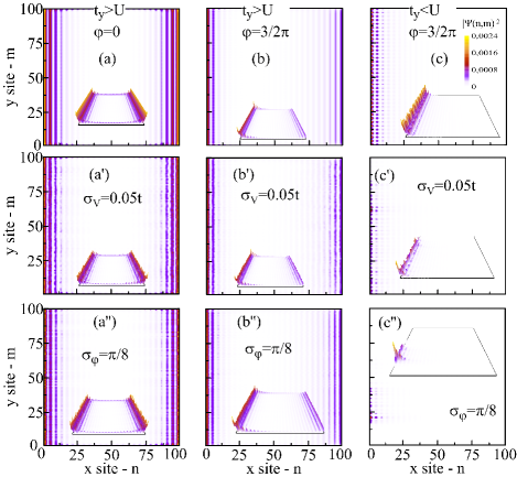
Disorder effects. In realistic systems one cannot avoid disorder. In our 2D finite size lattice model, we study effects of disorder by introducing (i) a random on-site potential and (ii) a random phase for the CDW modulation in each wire, i.e., . Here, () is taken according to a Gaussian distribution with zero mean and standard deviation (). By analyzing the edge state wave functions in different phases (see Fig. 4), we see that, for the given variance , the onsite disorder does not destroy the edge states in both topological [also the asymmetry in localization lengths is preserved, see Fig. 4 (b’)] and non-topological phases, see Figs. 4 (a’)-(c’) 111One can set the system parameters and disorder strength in such a way that only QHE edge states will survive.. Interestingly, chiral QHE edge states survive any amount of disorder in the phase , while in the non-topological phase, the edge states survive only up to a certain small amount of disorder with stronger disorder leading to Anderson localization around a random location along the edge.
Summary. We have studied a system of weakly coupled and CDW modulated wires in a perpendicular magnetic field. The system supports edge states in both the non-topological (CDW dominated) and topological (QHE dominated) phase. Interestingly, both phases host chiral and non-chiral edge states depending on the chemical potential position. Numerical calculations showed that, in general, the edge states in the non-topological phase are more affected by the disorder than in the topological phase, however, the former can still survive a finite amount of disorder. We propose that our predictions can be tested in semiconducting nanowires with CDW modulations, but also in optical lattices Lewenstein et al. (2007); Aidelsburger et al. (2013, 2015) or photonic crystals Kraus et al. (2012). Finally, it would be interesting to see if our results can be extended to other models which include TI phases with (piecewise) helical edge states.
Acknowledgements.
We acknowledge support from the Swiss NSF, NCCR QSIT, and SCIEX.References
- Klitzing et al. (1980) K. v. Klitzing, G. Dorda, and M. Pepper, Phys. Rev. Lett. 45, 494 (1980).
- Tsui et al. (1982) D. C. Tsui, H. L. Stormer, and A. C. Gossard, Phys. Rev. Lett. 48, 1559 (1982).
- Thouless et al. (1982) D. J. Thouless, M. Kohmoto, M. P. Nightingale, and M. den Nijs, Phys. Rev. Lett. 49, 405 (1982).
- Hasan and Kane (2010) M. Z. Hasan and C. L. Kane, Rev. Mod. Phys. 82, 3045 (2010).
- Hart et al. (2014) S. Hart, H. Ren, T. Wagner, P. Leubner, M. Mühlbauer, C. Brüne, H. Buhmann, L. W. Molenkamp, and A. Yacoby, Nature Physics (2014).
- Pribiag et al. (2015) V. S. Pribiag, A. J. Beukman, F. Qu, M. C. Cassidy, C. Charpentier, W. Wegscheider, and L. P. Kouwenhoven, Nature nanotechnology (2015).
- Spanton et al. (2014) E. M. Spanton, K. C. Nowack, L. Du, G. Sullivan, R.-R. Du, and K. A. Moler, Phys. Rev. Lett. 113, 026804 (2014).
- Wang et al. (2015) Y. H. Wang, J. R. Kirtley, F. Katmis, P. Jarillo-Herrero, J. S. Moodera, and K. A. Moler, Science 349, 948 (2015).
- Tamm (1932) I. Tamm, Z. Sowjetunion 1 (1932).
- Shockley (1939) W. Shockley, Phys. Rev. 56, 317 (1939).
- Gangadharaiah et al. (2012) S. Gangadharaiah, L. Trifunovic, and D. Loss, Phys. Rev. Lett. 108, 136803 (2012).
- Nichele et al. (2015) F. Nichele, H. J. Suominen, M. Kjaergaard, C. M. Marcus, E. Sajadi, J. A. Folk, F. Qu, A. J. Beukman, F. K. d. Vries, J. v. Veen, S. Nadj-Perge, L. P. Kouwenhoven, B.-M. Nguyen, A. A. Kiselev, W. Yi, M. Sokolich, M. J. Manfra, E. M. Spanton, and K. A. Moler, arXiv:1511.01728 (2015).
- Giamarchi (2003) T. Giamarchi, Quantum Physics in One Dimension, International Series of Monographs on Physics (Clarendon Press, 2003).
- Klinovaja and Loss (2014) J. Klinovaja and D. Loss, The European Physical Journal B 87, 171 (2014), 10.1140/epjb/e2014-50395-6.
- Bedell (1994) K. S. Bedell, in Proceedings held in Los Alamos, NM, 15-18 Dec. 1993 (1994) pp. 15–18.
- Algra et al. (2008) R. E. Algra, M. A. Verheijen, M. T. Borgström, L.-F. Feiner, G. Immink, W. J. van Enckevort, E. Vlieg, and E. P. Bakkers, Nature 456, 369 (2008).
- Deutschmann et al. (2001) R. A. Deutschmann, W. Wegscheider, M. Rother, M. Bichler, G. Abstreiter, C. Albrecht, and J. H. Smet, Phys. Rev. Lett. 86, 1857 (2001).
- Lebed (1986) A. Lebed, ZhETF Pisma Redaktsiiu 43, 137 (1986).
- Yakovenko (1991) V. M. Yakovenko, Phys. Rev. B 43, 11353 (1991).
- Klinovaja and Loss (2013a) J. Klinovaja and D. Loss, Phys. Rev. Lett. 111, 196401 (2013a).
- Teo and Kane (2014) J. C. Y. Teo and C. L. Kane, Phys. Rev. B 89, 085101 (2014).
- Klinovaja and Tserkovnyak (2014) J. Klinovaja and Y. Tserkovnyak, Phys. Rev. B 90, 115426 (2014).
- Seroussi et al. (2014) I. Seroussi, E. Berg, and Y. Oreg, Phys. Rev. B 89, 104523 (2014).
- Sagi and Oreg (2014) E. Sagi and Y. Oreg, Phys. Rev. B 90, 201102 (2014).
- Meng and Sela (2014) T. Meng and E. Sela, Phys. Rev. B 90, 235425 (2014).
- Klinovaja et al. (2015) J. Klinovaja, Y. Tserkovnyak, and D. Loss, Phys. Rev. B 91, 085426 (2015).
- Meng et al. (2015) T. Meng, T. Neupert, M. Greiter, and R. Thomale, Phys. Rev. B 91, 241106 (2015).
- Braunecker et al. (2010) B. Braunecker, G. I. Japaridze, J. Klinovaja, and D. Loss, Phys. Rev. B 82, 045127 (2010).
- Klinovaja and Loss (2012) J. Klinovaja and D. Loss, Phys. Rev. B 86, 085408 (2012).
- Alicea (2012) J. Alicea, Reports on Progress in Physics 75, 076501 (2012).
- Klinovaja et al. (2012) J. Klinovaja, P. Stano, and D. Loss, Phys. Rev. Lett. 109, 236801 (2012).
- Rainis et al. (2013) D. Rainis, L. Trifunovic, J. Klinovaja, and D. Loss, Phys. Rev. B 87, 024515 (2013).
- Jackiw and Rebbi (1976) R. Jackiw and C. Rebbi, Phys. Rev. D 13, 3398 (1976).
- Su et al. (1979) W. P. Su, J. R. Schrieffer, and A. J. Heeger, Phys. Rev. Lett. 42, 1698 (1979).
- Kivelson and Schrieffer (1982) S. Kivelson and J. R. Schrieffer, Phys. Rev. B 25, 6447 (1982).
- Klinovaja and Loss (2013b) J. Klinovaja and D. Loss, Phys. Rev. Lett. 110, 126402 (2013b).
- Note (1) In the Supplemental Material we consider higher filling factors and the dependence on the strip width.
- Wan et al. (2011) X. Wan, A. M. Turner, A. Vishwanath, and S. Y. Savrasov, Phys. Rev. B 83, 205101 (2011).
- Yang et al. (2011) K.-Y. Yang, Y.-M. Lu, and Y. Ran, Phys. Rev. B 84, 075129 (2011).
- Burkov and Balents (2011) A. A. Burkov and L. Balents, Phys. Rev. Lett. 107, 127205 (2011).
- Xu et al. (2011) G. Xu, H. Weng, Z. Wang, X. Dai, and Z. Fang, Phys. Rev. Lett. 107, 186806 (2011).
- Zyuzin and Burkov (2012) A. A. Zyuzin and A. A. Burkov, Phys. Rev. B 86, 115133 (2012).
- Baum et al. (2015) Y. Baum, T. Posske, I. C. Fulga, B. Trauzettel, and A. Stern, Phys. Rev. Lett. 114, 136801 (2015).
- Note (2) One can set the system parameters and disorder strength in such a way that only QHE edge states will survive.
- Lewenstein et al. (2007) M. Lewenstein, A. Sanpera, V. Ahufinger, B. Damski, A. Sen, and U. Sen, Advances in Physics 56, 243 (2007).
- Aidelsburger et al. (2013) M. Aidelsburger, M. Atala, M. Lohse, J. T. Barreiro, B. Paredes, and I. Bloch, Phys. Rev. Lett. 111, 185301 (2013).
- Aidelsburger et al. (2015) M. Aidelsburger, M. Lohse, C. Schweizer, M. Atala, J. T. Barreiro, S. Nascimbene, N. Cooper, I. Bloch, and N. Goldman, Nature Physics 11, 162 (2015).
- Kraus et al. (2012) Y. E. Kraus, Y. Lahini, Z. Ringel, M. Verbin, and O. Zilberberg, Phys. Rev. Lett. 109, 106402 (2012).
Appendix A Dependence on the width of the strip.
In the numerical results presented in the main part, the number of lattice sites is chosen to cover an integer number of Fermi wavelengths inside the strip. As a result, the discretized CDW potential has an inversion symmetry point for . However, one can choose the number of sites such that the length of the wire (i.e., the width of the strip) corresponds to a half integer number of Fermi wavelengths. In this case the CDW phase shift at the right end of the strip is different from those in the main text, see Fig. 5. As expected, the left edge modes are not affected by this new choice, but the dispersion of the right edge mode is changed. For example, the discretized CDW potential has now an inversion symmetry point for the phase value . Interestingly, in the non-topological phase, , one can find again non-chiral edge states that do not touch the bulk modes. The 2D wave functions for both edge states present in the non-topological regime are depicted in the Fig. 6.

Appendix B Filling factor .
One can also observe phase transitions similar to the ones descibed in the main text for for the filing factor , which corresponds to an indirect resonant magnetic field with Klinovaja and Loss (2013a, 2014). In this case, the size of the gap opened by the resonant scattering is smaller () than for the case and the phase transitions occurs for correspondingly smaller . In the topological phase (, ), there are always two chiral edge states present at each edge, see Figs. 3 (a)-(b). Interestingly, in the non-topological phase (, ), there can be two or four modes present at the same edge, see Fig. 7(b’).