Few-layer Phosphorene: An Ideal 2D Material For Tunnel Transistors
Abstract
2D transition metal dichalcogenides (TMDs) have attracted a lot of attention recently for energy-efficient tunneling-field-effect transistor (TFET) applications due to their excellent gate control resulting from their atomically thin dimensions. However, most TMDs have bandgaps () and effective masses () outside the optimum range needed for high performance. It is shown here that the newly discovered 2D material, few-layer phosphorene, has several properties ideally suited for TFET applications: 1) direct in the optimum range 1.0-0.4 eV, 2) light transport (0.15), 3) anisotropic which increases the density of states near the band edges, and 4) a high mobility. These properties combine to provide phosphorene TFET outstanding 1 mA/um, ON/OFF ratio106, scalability to 6 nm channel length and 0.2 V supply voltage, thereby significantly outperforming the best TMD-TFETs in energy-delay products. Full-band atomistic quantum transport simulations establish phosphorene TFETs as serious candidates for energy-efficient and scalable replacements of MOSFETs.
Keywords— 2D TFETs, Phosphorene , NEGF, Scaling theory, Band to band tunneling.
Metal-Oxide-Semiconductor Field-Effect-Transistors (MOSFETs) have been the workhorse of most modern-day electronics. Although aggressive size scaling of MOSFETs have ushered in an era of ultra-fast miniature electronics, the advantages of scaling are fast disappearing as MOSFETs enter the sub-20 nm regime. In state-of-the-art MOSFETs, direct source to drain tunneling through the channel potential barrier degrades the OFF-state current and causes excessive power dissipation [1]. Tunnel FETs (TFETs) have been proposed to be energy-efficient alternatives to the MOSFET that can reduce the supply voltage () and satisfy the low power requirements in integrated circuits [2, 3]. Although TFETs, in principle, provide a steep OFF to ON transition needed to minimize power dissipation, the ON-currents of TFETs are quite low [4, 5], which deteriorates their operational speed and energy-delay product [6]. The current level in TFETs is the result of band to band tunneling (BTBT) of carriers, and hence, highly sensitive to the effective masses () and bandgaps () of the channel material. While a small and improve the ON-current () and supply voltage scaling, the same also deteriorate the OFF-current and channel length () scaling through direct source-to-drain tunneling [7]. To meet the simultaneous requirement of the semiconductor industry of both power supply and size scaling, materials need to be carefully chosen with optimized and . In this work, it is shown that the newly studied few-layer phosphorene [8] provides the ideal material properties to obtain high performance in TFETs as well as to simultaneously achieve both and scaling.
There are several solutions to the low challenge of TFETs [4]. depends exponentially on , , and the electric field at tunnel junction (i.e. ). Hence, can be enhanced either by a) increasing or by b) using a channel material with optimum and . A number of approaches for increasing the electric field were proposed before such as 1) atomically thin 2D channel materials that provide a tight gate control and small tunneling distance [9, 10, 4], 2) dielectric engineering with high- and low-k spacers [11, 12], 3) internal polarization in Nitrides [13].
In addition to having an atomically thin channel that improves F, few-layer phosphorene also has the optimum and required for high performance TFETs. Moreover, the bandgap of phosphorene remains direct as the number of layers increases. In this regard, phosphorene has a great advantage over other 2D materials, such as graphene and transition metal dichalcogenides (TMDs). Graphene lacks a bandgap and even with engineered bandgaps, it remains unsuitable for transistor applications [14]. Most monolayer TMDs have a bandgap larger than 1 eV. While the Eg of some multi-layer TMDs may reach below 1 eV, multi-layer TMDs are usually indirect gap materials in which the requirement of momentum change of the carriers by phonons causes very low ON-currents. Among TMDs, only WTe2 in 2H phase has a moderate of 0.75 eV, however it suffers from a large [15], and the 2H phase of WTe2 has not been experimentally demonstrated yet. Density Functional Theory (DFT) calculations predict that of phosphorene varies from about 1.4 eV in monolayer to 0.3 eV in bulk[16]. Also, phosphorene has lighter for both electrons and holes of 0.15 . Hence, phosphorene is expected to provide the highest performance among all the 2D material TFETs considered so far.
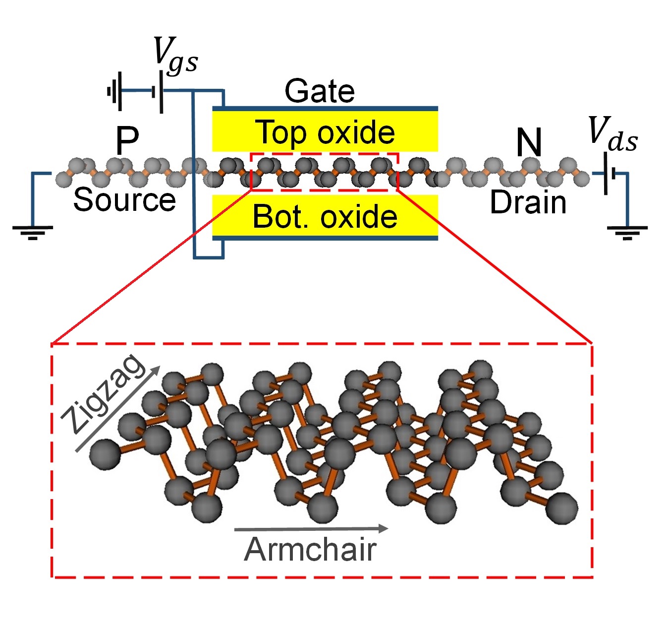
In a few-layer phosphorene flake, each layer is a hexagonal honey comb lattice with puckered surface, as shown in Fig. 1a. The electron and hole effective masses are highly anisotropic; is low in the armchair direction ( 0.15 ) and is very high in the zigzag direction ( 1 )[16]. Since the tunneling probability decreases exponentially with the transport effective mass [17], it is best to have the channel oriented along the armchair direction for high . In such a case, the very large in the transverse zigzag direction results in a high density of states near the band edges. This anisotropy ultimately leads to a large , as shown later in the paper. The scaling of TFETs to the sub-10 nm regime also require engineering and to keep the ON and OFF state performance intact [7]. However, to achieve this in most conventional materials such as III-Vs, complicated experimental techniques need to adopted such as application of strain or forming alloys, which can also introduce disorder in the device. In this regard, the layer dependent and in phosphorene already provides an additional knob to optimize the performance for sub-10 nm TFETs, as shown later.
Experimentally, phosphorene flakes as thin as a single layer have been realized recently by means of mechanical exfoliation [8]. The experimental of a single layer phosphorene has been measured to be approximately 1.45 eV which is way higher than the bulk of black phosphorus ( 0.3 eV). Measured few-layer phosphorene carrier mobility is very high in the armchair direction, it is 256 cm2/Vs for few-layers and 1000 cm2/Vs for bulk [8]. In addition, strong anisotropy of was verified by angle dependent conductivity [8]. Later, Saptarshi et al. reported experimental measurements of the thickness dependent transport gap and Schottky barriers of phosphorene [18]. However, there are challenges to the development of phosphorene based electronics as well. Few-layer phosphorene is unstable in atmosphere and is prone to humidity and oxygen. Hence, it degrades within several hours when left in air[19, 20]. However, there are many efforts to solve this stability challenge; e.g. Junhong et al. stabilized phosphorene for two months by encapsulating it within [21].
In this work, we performed full band atomistic quantum transport simulations of phosphorene TFETs based on the non-equilibrium Green’s function simulator NEMO5 with a second nearest neighbor sp3d5s∗ tight-binding (TB) Hamiltonian. The electrostatics of the device is obtained by solving a 3D finite-element Poisson equation self-consistently with the quantum transport equations described in the Methods section. The simulated phosphorene TFET assumes a double gated structure as shown in Fig. 1a. The channel length is 15 nm and the transport direction is oriented along the armchair direction. The source and drain doping levels are set to cm-3 in a p-i-n configuration, effective oxide thickness (EOT) is 0.5 nm, and the drain bias equals 0.5 V unless mentioned otherwise. The device specifications are compatible with the international technology road-map for semiconductors (ITRS) projections for 2027 [22].
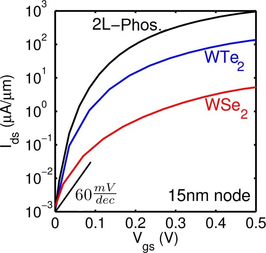
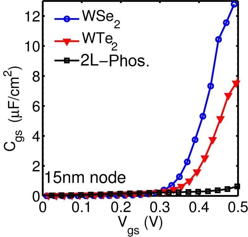
Figs. 1b and 1c compare the current-voltage () and capacitance-voltage () characteristics respectively of bilayer-phosphorene (2L-phosphorene) with those of WTe2 and WSe2 (which have been identified as the best TMD material candidates for TFETs [15]) for a supply voltage of 0.5 V. 2L-phosphorene provides an inverse sub-threshold slope (SS) much lower than the other two TMDs (well below the Boltzmann limit of 60 mV/dec at room temperature), and provides an of nearly 1 mA/um (about 7.5 times higher than WTe2 in 2H phase). The ON-state capacitance of 2L-phosphorene is also about 5 times lower than that of WTe2. The large and small and translate into a very small switching energy and switching delay for the 2L-phosphorene. The most important metric of performance for low power transistors is the product of the switching energy and the delay (energy-delay product or EDP) [6]. The lower the EDP, the more energy-efficient and faster the device is. 2L-phosphorene has 176 times lower EDP compared to the best TMD TFET (WTe2). The origins of these improvements are discussed next.
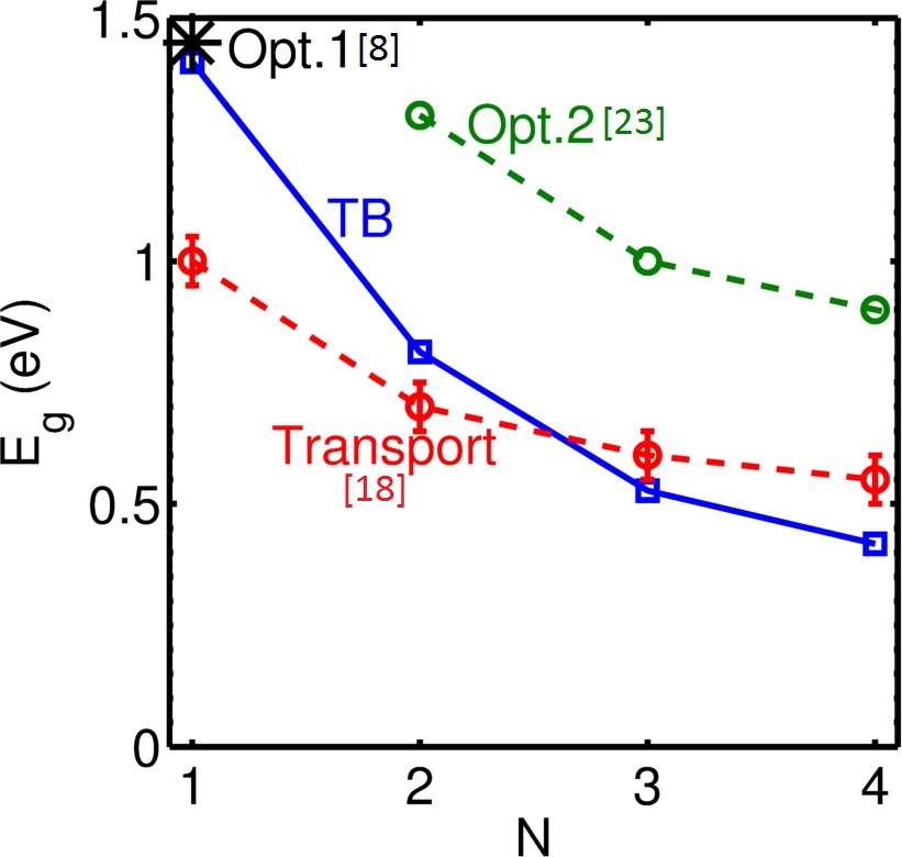
Figs. 2a and 2b show and in the armchair direction () as a function of the number of phosphorene layers extracted from phosphorene bandstructures computed with the atomistic tight-binding model of this work. In Ref. [7], optimum and values needed to maximize in TFETs were presented for various supply voltages and channel lengths . It was suggested that for 15 nm and 0.5 V, and need to be roughly about 0.7 V and 0.15 respectively. It is seen in Fig. 2b that the electron and hole are roughly about 0.15 and do not vary much with the number of layers. While the in Fig. 2a is seen to be strongly dependent on the number of layers, apart from the 1.4 eV value for monolayer phosphorene, is mostly in the range of 0.7 to 0.4 eV, with the optimum value of 0.7 eV reached for 2L-phosphorene. It is to be noted that there is still some experimental discrepancy about the actual values of in phosphorene with transport measurements yielding smaller bandgaps than optical measurements (as also seen in TMDs). On the other hand, DFT and DFT-guided TB calculations used in this work yield bandgaps closer to the transport measurements. In spite of these differences, the layer dependent variation of from the bulk value of 0.4 eV suggests enough scope to optimize by varying the channel thickness.

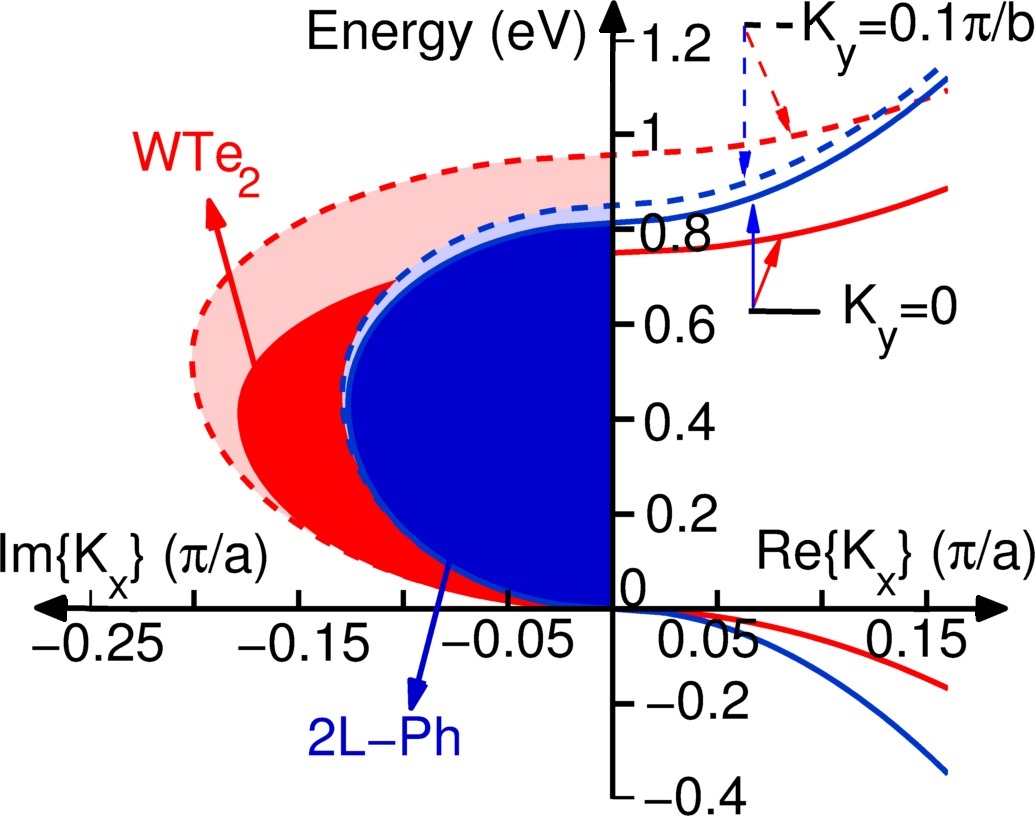
The bandgap alone does not explain why the phosphorene TFET significantly outperforms WTe2 TFET since 2L-phosphorene has a similar as 1L-WTe2. The difference actually originates from 2L-phosphorene having a light transport in the armchair direction () and a heavy transverse in the zigzag direction (). This is conveniently illustrated in the complex bandstructure in Fig. 2c, which shows the energy-momentum dispersion of the carriers in the forbidden bandgap connecting the conduction and valence band states. The complex part of the bandstructure corresponds to the evanescent wavefunctions in the bandgap with imaginary momentum , and the area enclosed by the imaginary band and the energy axis corresponds to the band to band tunneling (BTBT) decay rate [24]. The smaller the area, the larger is the transmission probability. Fig. 2c compares the complex band structure of 2L-phosphorene with 1L-WTe2. The complex bands are plotted at transverse wave-vector and for both materials. 2L-phosphorene not only has a smaller BTBT decay rate at (due to small transport ), but also at a non-zero . This is due to a large transverse () which prevents the decay rate from increasing significantly with . In other words, phosphorene has a high density of states of carriers with optimum transport and .
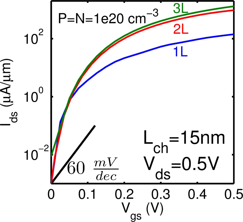
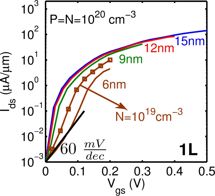
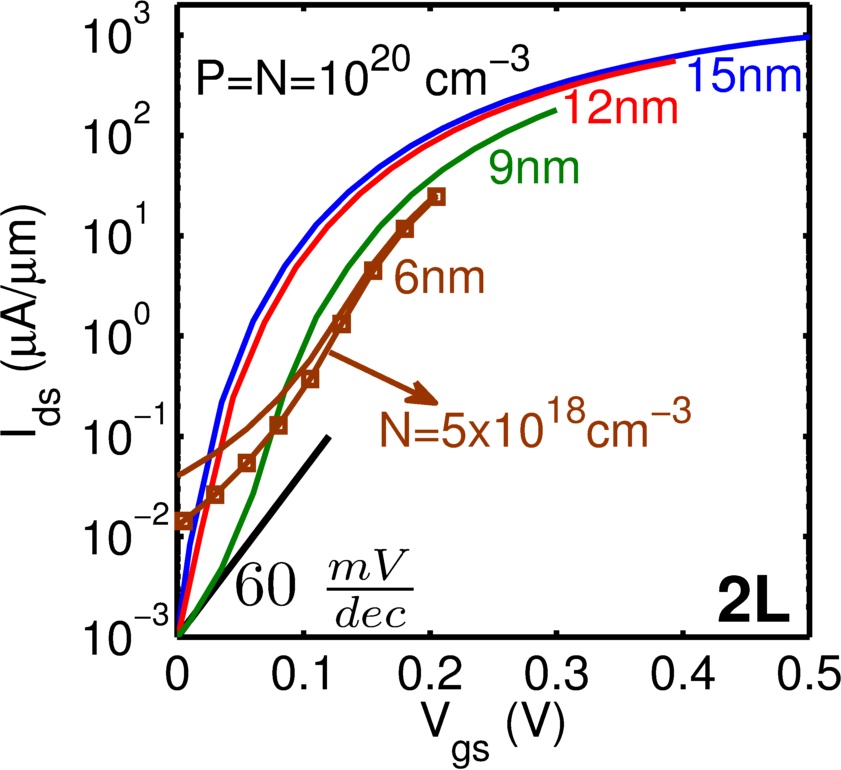
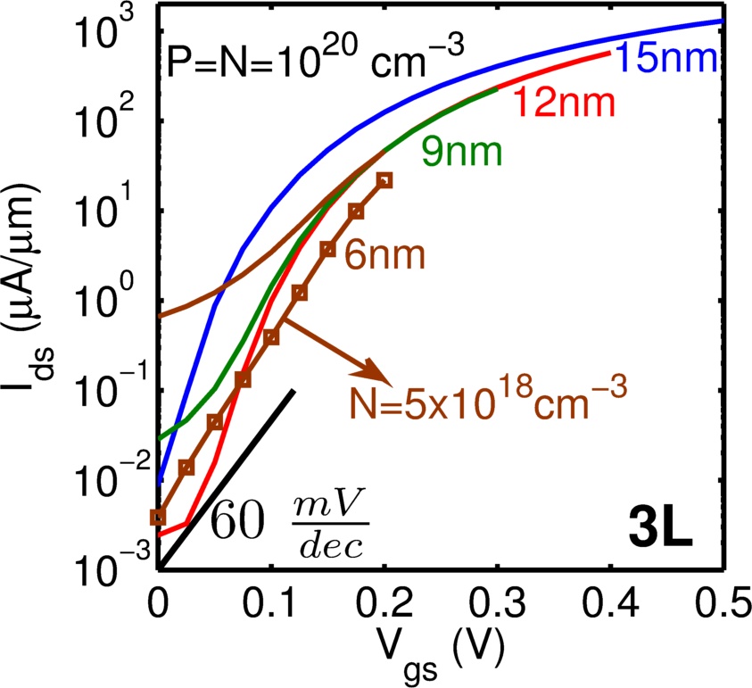
Next, the performance of the phosphorene TFET and its scalability in and are evaluated as a function of the number of layers. Fig. 3a shows the transfer characteristics of mono- (1L), bi- (2L), and tri-layer (3L) phosphorene TFETs with of 15 nm. The 2L-phosphorene provides the highest ON/OFF current ratio. Notice that although 3L phosphorene provides higher , it has a higher compared to the 2L case. Fig. 3b to 3d show the transfer characteristics of scaled few-layer phosphorene at different technology nodes. Constant electric field scaling (i.e. ) of 30 V/nm is considered here. Doping level of source and drain is assumed to be symmetric unless mentioned otherwise. In almost all of the three cases, the phosphorene TFET seems to scale very well from 15 nm to 9 nm channel lengths. Although for very short such as 6 nm, degrades significantly, asymmetric doping can be used to suppress the p-branch of the TFET and reduce . For the = 6 nm case, reducing the drain doping () increases the drain to channel tunneling distance [25] and helps to block . However, there is a lower limit to . Reducing reduces the carrier density (through ) and the tunneling window. For the = 6 nm case, the optimum is found to be cm-3 in 1L, and cm-3 in 2L and 3L as shown in Fig. 3 b-d). 1L case shows the highest ON/OFF current ratio in the 6 nm case.
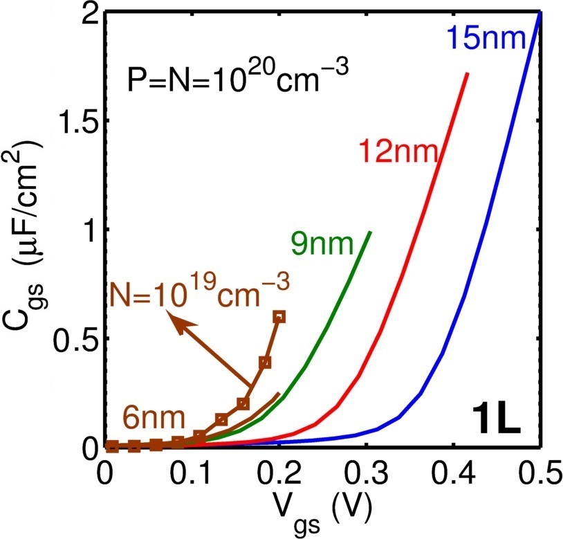
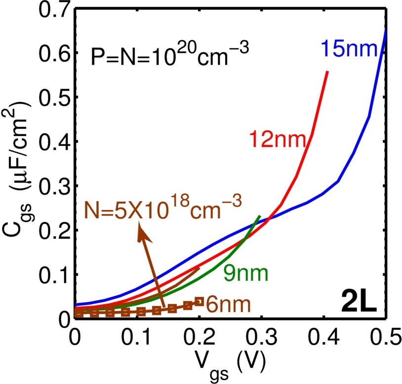
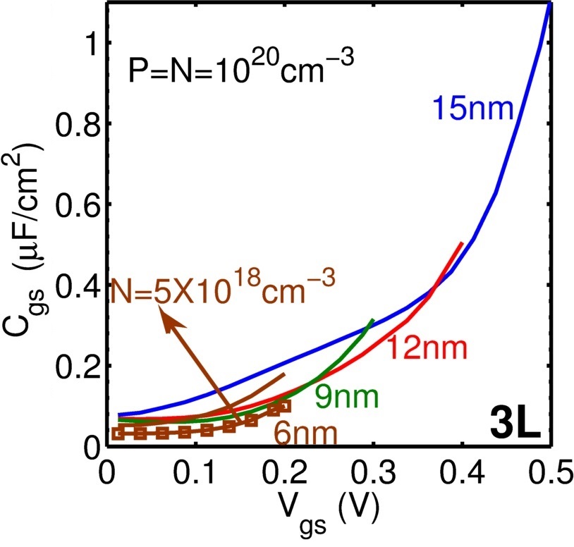
The total gate capacitances () of 1L- to 3L-phosphorene TFETs are shown in Fig. 4 for the same constant electric field scaling discussed before. As expected, the capacitances also scale quite well up to 9 nm. 2L-phosphorene offers the lowest capacitances. Although the capacitances for the = 6 nm case are slightly larger than the 9 nm case, asymmetric doping can decrease the capacitance for 2L and 3L, as shown Fig. 4. The capacitances predicted here for phosphorene are much less () than those reported for TMDs [15]. The lower in phosphorene originates from its optimum and . The - and - are shifted in voltage axis such that the current at zero gate voltage is set to 1 nA/um as required by ITRS [22]. Lower currents in TMDs, which is a result of their higher and , makes 0 gate voltage to be closer to threshold voltage if compared with phosphorene. Accordingly, TMDs operate closer to ON-state which results in a higher amount of charge in channel and a higher . In summary, the benefits of optimum , small transport , and large transverse in phosphorene are two-fold: 1) higher , and 2) lower capacitance.
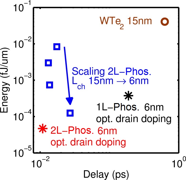
The outstanding - and - characteristics of few-layer phosphorene translate into impressive energy-delay products, which is used ultimately to compare ultra-fast energy-efficient transistors. Fig. 5 shows the computed intrinsic energy and delay of phosphorene TFETs compared to WTe2, which has been benchmarked as the best TMD TFET [15]. It has been shown that WTe2 also outperforms complementary (C) MOS low power FETs in a simulation of the extrinsic delay of a 32 bit full adder [15]. In a plot of energy versus delay such as Fig. 5, the bottom left corner with the lowest EDP is preferred. It is seen in Fig. 5 that the EDPs of phosphorene TFETs are much smaller than the best TMD TFET. EDP of 2L-phosphorene with of 15 nm is two orders of magnitude smaller than the EDP of the WTe2 TFET. Not only does phosphorene provide record and but also a record energy delay product among 2D materials. The optimized asymmetric doping also improves the energy delay product of TFETs specially for sub-9 nm channel lengths.
In conclusion, few-layer phosphorene has a unique set of properties which makes it an excellent candidate for future ultra-scaled low power electronics: 1) atomistically thin body thickness, 2) tune-able and with number of layers within the optimum range for TFET applications, 3) anisotropic , and 4) direct band gap even in multi-layer. These features make phosphorene an exceptional candidate among 2D materials for TFET applications. The - and - characteristics of few-layer phosphorene exhibit orders of magnitude improvement in energy-delay product compared to other 2D TFETs (e.g. TMD TFETs). Bilayer phosphorene shows optimum performance and is recommended for adoption as the future material of 2D-TFETs.
Methods
In the quantum transport simulations performed in this work, the phosphorene Hamiltonian employs a 10 band sp3d5s∗ 2nd nearest neighbor tight binding model (TB). The TB parameters have been optimized to reproduce the band structures obtained from density functional theory (DFT) using HSE06. A general TB parameter set was obtained that captured the bandstructure of monolayer to bulk phosphorene. This DFT to TB mapping is a standard technique in semi-empirical TB [26]. The Hamiltonian is represented with TB instead of DFT, since DFT is computationally expensive and is size limited. Our TB model agrees well with previous calculations of and of few-layer phosphorene obtained from DFT with Becke Johnson functional (DFT-mBJ)[16]
For transport simulations, a self- consistent Poisson-quantum transmitting boundary method (QTBM) has been used with the TB Hamiltonian. QTBM is equivalent to the non equilibrium Green’s function (NEGF) approach in the ballistic case, but it entails the solution of a linear system of equations instead of obtaining the Green’s function by matrix inversion which is more computationally inefficient [27]. In QTBM, the Schroedinger equation with open boundary conditions is given as,
| (1) |
where , , , and are the carrier energy, identity matrix, device Hamiltonian, and self-energy due to open boundaries and and S are the wave function and a carrier injection term respectively from either source (S) or drain (D). 3D Poisson equation is solved using the finite-element method. It should be noted that the dielectric tensor of few-layer phosphorene is anisotropic and has been obtained from DFT calculations [28]. The Poisson equation reads as follows :
| (2) |
where and are the electrostatic potential and total charge, respectively. In this paper, the transport simulations have been performed with the Nanoelectronics Modeling tool NEMO5[29, 30].
References
- [1] A. M. Ionescu and H. Riel, “Tunnel field-effect transistors as energy-efficient electronic switches,” Nature, vol. 479, no. 7373, pp. 329–337, 2011.
- [2] J. Appenzeller, Y.-M. Lin, J. Knoch, and P. Avouris, “Band-to-band tunneling in carbon nanotube field-effect transistors,” Physical Review Letters, vol. 93, no. 19, p. 196805, 2004.
- [3] J. Appenzeller, Y.-M. Lin, J. Knoch, Z. Chen, and P. Avouris, “Comparing carbon nanotube transistors-the ideal choice: a novel tunneling device design,” Electron Devices, IEEE Transactions on, vol. 52, no. 12, pp. 2568–2576, 2005.
- [4] D. Sarkar, X. Xie, W. Liu, W. Cao, J. Kang, Y. Gong, S. Kraemer, P. M. Ajayan, and K. Banerjee, “A subthermionic tunnel field-effect transistor with an atomically thin channel,” Nature, vol. 526, no. 7571, pp. 91–95, 2015.
- [5] W. Y. Choi, B.-G. Park, J. D. Lee, and T.-J. K. Liu, “Tunneling field-effect transistors (tfets) with subthreshold swing (ss) less than 60 mv/dec,” Electron Device Letters, IEEE, vol. 28, no. 8, pp. 743–745, 2007.
- [6] D. Nikonov and I. Young, “Benchmarking of beyond-cmos exploratory devices for logic integrated circuits,” Exploratory Solid-State Computational Devices and Circuits, IEEE Journal on, vol. 1, pp. 3–11, Dec 2015.
- [7] H. Ilatikhameneh, G. Klimeck, and R. Rahman, “Can tunnel transistors scale below 10nm?,” IEEE Electron Device Letters, DOI: 10.1109/LED.2015.2501820., 2015.
- [8] H. Liu, A. T. Neal, Z. Zhu, Z. Luo, X. Xu, D. Tománek, and P. D. Ye, “Phosphorene: an unexplored 2d semiconductor with a high hole mobility,” ACS nano, vol. 8, no. 4, pp. 4033–4041, 2014.
- [9] G. Fiori, F. Bonaccorso, G. Iannaccone, T. Palacios, D. Neumaier, A. Seabaugh, S. K. Banerjee, and L. Colombo, “Electronics based on two-dimensional materials,” Nature nanotechnology, vol. 9, no. 10, pp. 768–779, 2014.
- [10] Q. Zhang, G. Iannaccone, and G. Fiori, “Two-dimensional tunnel transistors based on thin film,” Electron Device Letters, IEEE, vol. 35, no. 1, pp. 129–131, 2014.
- [11] H. Ilatikhameneh, T. Ameen, G. Klimeck, J. Appenzeller, and R. Rahman, “Dielectric engineered tunnel field-effect transistor,” Electron Device Letters, IEEE, vol. 36, pp. 1097–1100, Oct 2015.
- [12] F. W. Chen, H. Ilatikhameneh, G. Klimeck, Z. Chen, and R. Rahman, “Configurable electrostatically doped high performance bilayer graphene tunnel fet,” arXiv preprint arXiv:1509.03593, 2015.
- [13] W. Li, S. Sharmin, H. Ilatikhameneh, R. Rahman, Y. Lu, J. Wang, X. Yan, A. Seabaugh, G. Klimeck, D. Jena, and P. Fay, “Polarization-engineered iii-nitride heterojunction tunnel field-effect transistors,” Exploratory Solid-State Computational Devices and Circuits, IEEE Journal on, vol. 1, pp. 28–34, Dec 2015.
- [14] Y. Zhang, T.-T. Tang, C. Girit, Z. Hao, M. C. Martin, A. Zettl, M. F. Crommie, Y. R. Shen, and F. Wang, “Direct observation of a widely tunable bandgap in bilayer graphene,” Nature, vol. 459, no. 7248, pp. 820–823, 2009.
- [15] H. Ilatikhameneh, Y. Tan, B. Novakovic, G. Klimeck, R. Rahman, and J. Appenzeller, “Tunnel field-effect transistors in 2-d transition metal dichalcogenide materials,” Exploratory Solid-State Computational Devices and Circuits, IEEE Journal on, vol. 1, pp. 12–18, Dec 2015.
- [16] J. Qiao, X. Kong, Z.-X. Hu, F. Yang, and W. Ji, “High-mobility transport anisotropy and linear dichroism in few-layer black phosphorus,” Nature communications, vol. 5, 2014.
- [17] H. Ilatikhameneh, R. B. Salazar, G. Klimeck, R. Rahman, and J. Appenzeller, “From fowler-nordheim to non-equilibrium green’s function modeling of tunneling,” arXiv preprint arXiv:1509.08170, 2015.
- [18] S. Das, W. Zhang, M. Demarteau, A. Hoffmann, M. Dubey, and A. Roelofs, “Tunable transport gap in phosphorene,” Nano letters, vol. 14, no. 10, pp. 5733–5739, 2014.
- [19] A. Castellanos-Gomez, L. Vicarelli, E. Prada, J. O. Island, K. Narasimha-Acharya, S. I. Blanter, D. J. Groenendijk, M. Buscema, G. A. Steele, J. Alvarez, et al., “Isolation and characterization of few-layer black phosphorus,” 2D Materials, vol. 1, no. 2, p. 025001, 2014.
- [20] L. Kou, C. Chen, and S. C. Smith, “Phosphorene: Fabrication, properties, and applications,” The journal of physical chemistry letters, vol. 6, no. 14, pp. 2794–2805, 2015.
- [21] J. Na, Y. T. Lee, J. A. Lim, D. K. Hwang, G.-T. Kim, W. K. Choi, and Y.-W. Song, “Few-layer black phosphorus field-effect transistors with reduced current fluctuation,” ACS nano, vol. 8, no. 11, pp. 11753–11762, 2014.
- [22] “International technology roadmap for semiconductors (itrs).” http://www.itrs.net, 2013.
- [23] S. Zhang, J. Yang, R. Xu, F. Wang, W. Li, M. Ghufran, Y.-W. Zhang, Z. Yu, G. Zhang, Q. Qin, et al., “Extraordinary photoluminescence and strong temperature/angle-dependent raman responses in few-layer phosphorene,” ACS nano, vol. 8, no. 9, pp. 9590–9596, 2014.
- [24] X. Guan, D. Kim, K. C. Saraswat, and H.-S. P. Wong, “Complex band structures: From parabolic to elliptic approximation,” Electron Device Letters, IEEE, vol. 32, no. 9, pp. 1296–1298, 2011.
- [25] R. B. Salazar, H. Ilatikhameneh, R. Rahman, G. Klimeck, and J. Appenzeller, “A predictive analytic model for high-performance tunneling field-effect transistors approaching non-equilibrium green's function simulations,” Journal of Applied Physics, vol. 118, no. 16, pp. –, 2015.
- [26] Y. P. Tan, M. Povolotskyi, T. Kubis, T. B. Boykin, and G. Klimeck, “Tight-binding analysis of si and gaas ultrathin bodies with subatomic wave-function resolution,” Physical Review B, vol. 92, no. 8, p. 085301, 2015.
- [27] M. Luisier, A. Schenk, W. Fichtner, and G. Klimeck, “Atomistic simulation of nanowires in the s p 3 d 5 s* tight-binding formalism: From boundary conditions to strain calculations,” Physical Review B, vol. 74, no. 20, p. 205323, 2006.
- [28] V. Wang, Y. Kawazoe, and W. Geng, “Native point defects in few-layer phosphorene,” Physical Review B, vol. 91, no. 4, p. 045433, 2015.
- [29] S. Steiger, M. Povolotskyi, H.-H. Park, T. Kubis, and G. Klimeck, “Nemo5: a parallel multiscale nanoelectronics modeling tool,” Nanotechnology, IEEE Transactions on, vol. 10, no. 6, pp. 1464–1474, 2011.
- [30] J. E. Fonseca, T. Kubis, M. Povolotskyi, B. Novakovic, A. Ajoy, G. Hegde, H. Ilatikhameneh, Z. Jiang, P. Sengupta, Y. Tan, et al., “Efficient and realistic device modeling from atomic detail to the nanoscale,” Journal of Computational Electronics, vol. 12, no. 4, pp. 592–600, 2013.
Acknowledgment
This work was supported in part by the Center for Low Energy Systems Technology (LEAST), one of six centers of STARnet, a Semiconductor Research Corporation program sponsored by MARCO and DARPA. nanoHUB.org computational resources are used. operated by the Network for Computational Nanotechnology funded by the US National Science Foundation under grant EEC-1227110, EEC-0228390, EEC-0634750, OCI-0438246, and OCI-0721680 is gratefully acknowledged.
Author Contributions
T.A and H. I. performed the simulations and analyzed the data. G. K. and R.R. supervised the work. All authors contributed to writing the manuscript.
Competing financial interests
The authors declare no competing financial interests.