The consequences of dependence between the formal area efficiency and the macroscopic electric field on linearity behavior in Fowler-Nordheim plots
Abstract
This work presents a theoretical explanation for a crossover in the linear behavior in Fowler-Nordheim (FN) plots based on cold field electron emission (CFE) experimental data. It is characterized by a clear change in the decay rate of usually single-slope FN plots, and has been reported when non-uniform nano-emitters are subject to high macroscopic electric field . We assume that the number of emitting spots, which defines an apparent formal area efficiency of CFE surfaces, depends on the macroscopic electric field. Non-uniformity is described by local enhancement factors , which are randomly assigned to each distinct emitter of a conducting CFE surface, from a discrete probability distribution , with . It is assumed that , and that . The local current density is evaluated by considering a usual Schottky-Nordheim barrier. The results reproduce the two distinct slope regimes in FN plots when V/m and are analyzed by taking into account the apparent formal area efficiency, the distribution , and the slopes in the corresponding FN plot. Finally, we remark that our results from numerical solution of Laplace’s equation, for an array of conducting nano-emitters with uniform apex radii nm but different local height, supports our theoretical assumptions and could used in orthodox CFE experiments to test our predictions.
I Introduction
Understanding the role of the morphology of large area field electron emitters (LAFEs) is of utmost importance to better explore their potential applications. Typical field emitter arrays consist of regular two-dimensional patterns of individual, similar, and small size field electron emitters, which may be prepared by lithographic techniques MC . The best known LAFE devices are the Spindt arrays, in which each individual field emitter is a small sharp molybdenum cone Spindt . Unfortunately, there are some inconveniences of using Spindt-type metal arrays for vacuum microelectronic devices due the expensive production, the critical lifetime in technical vacuum and the high operating voltages Oliver . Moreover, poor tip-to-tip reproducibility caused by the presence of nano-protrusions, which are also present in other nonmetallic arrays, makes it difficult to accurately predict their emission characteristics. To sidestep some of these difficulties, the cold field emission (CFE) community redirected efforts to study and produce different purpose LAFEs as nano-electronic devices, including carbon nano-structures which have near-ideal whisker-like shapes with hemispherical tips Cole . This choice is justified by a set of favorable properties like nanometer size tip, high chemical inertness, high electrical and thermal conductivity, and low manufacturing costs Oliver .
A relevant issue relating experimental and theoretical aspects of CFE studies is how to assess, with sufficient technologic reliability, several quantities related to the LAFE efficiency from measurable current-voltage characteristics. This is usually done using Fowler-Nordheim (FN) plots, which relates the macroscopic current density to the applied (or macroscopic) electric field . The theory leading to Fowler-Nordheim-type (FN-type) equations suggests to draw FN-plots consisting of curves for vs , but other variable combinations can be used as well (see for instance Ref. MC ). Actually, FN-plots may present a non-linear behavior and is necessary to set up a convenient theory that takes into account more realistic conditions under which a specific CFE experiment is performed in order to obtain a correct interpretation of the field enhancement factor (FEF) and other experimental outputs Cahay . In this context, it’s important to discuss some general definitions as follow: the slope characterization parameter (alternatively called apparent FEF) is defined by
| (1) |
where is the slope of a sufficient linear FN-plot, for a given range of , is the local work-function of the emitter, and is the second Fowler-Nordheim (FN) constant eV-3/2 V nm-1); the actual characteristic FEF, , is defined as
| (2) |
where is the characteristic local barrier field. Then, the general relationship between and has the form
| (3) |
where is the relevant generalized slope correction factor.
Some situations can display nonlinear behavior in the corresponding FN-plots. This can be observed already in the pioneer work by Lauritsen who, in this Ph. D. thesis obtained plots of the form vs Voltage, where is the macroscopic current emitted. He found experimentally that plots of the form vs Voltage may be consisted of two straight lines, with a slight kink in the middle, using a cylindrical wire geometry Lauritsen (see, for instance, Figs. 6 and 12 of that work). Another example is related to the particular condition in which a large series resistance is found in the circuit between the high-voltage generator and the emitter’s regions. The interpretation of corresponding FN-plots was provided by Forbes and collaborators FNReport . For both LAFE and single tip field emitters (STFEs), they showed that if the so-called CFE orthodox emission hypotheses Forbes1 are not satisfied, the analysis of the results based on the elementary FN equation, as usually performed by experimentalists, can generate a spurious estimates for the true electrostatic FEF AuPost ; Forbes1 . On the other hand, recent theoretical works by one of authors deAssis12015 ; deAssis22015 explained how a slight positive curvature on FN-plots arises when a dependency between the apparent formal area efficiency () and is taken into account. For some assumptions of non-uniform conditions in the LAFES morphology, which amounts to consider a local FEF () probability distribution with exponential or Gaussian behavior, the orthodoxy test showed does not fail for practical circumstances. Despite this, it was possible to suggest experimental tests that can verify the proposed correction to the values with statistical significance.
In this work, the authors investigate the conditions under which a clear crossover on the FN plots of CFE may appear, by assuming that it is only a consequence of the dependency between and . The electron emission from a conduction band on a particular LAFE location is described by FN-type equations with a Schottky–Nordheim (SN) barrier. Different from Refs. deAssis12015 ; deAssis22015 , which considered continuous distributions, the present model assumes CFE through a non-uniform distribution of the local FEF on LAFE surface, which is described by a discrete asymmetric bimodal distribution for two distinct values and , with and . So, let us define
| (4) |
and
| (5) |
The characteristic FEF of the LAFE is . From now on, whenever we mention this specific model we will indicate the characteristic FEF as , while will be used to refer to FEF in general conditions. Depending on the bimodal asymmetry parameter , this contribution may lead to a clear crossover effect in the corresponding FN plots. Our results suggest that this simple mechanism, mimicking fluctuations of the individual emitter morphology on a LAFE surface, can justify a pronounced change in FN plots only as the emission is orthodox.
This paper is organized as follows. In Sec. II, the model and the equations for computing the local current density are presented. We put this in perspective of previous studies discussing nonlinear behavior in the corresponding current-voltage measurements. Results are presented in Sec. III, focusing on the conditions where nonlinear FN plots can be found. We also discuss the results from numerical solution of Laplace’s equation, using an array of conducting nano-emitters with large apex radii ( nm) but different heights. In Sec. IV, the main conclusions are presented.
II Current density calculations, model and previous works
The interpretation of experimental CFE outputs have often been done using the elementary FN-type equation, hereafter referred to as “elementary” equations and theory, which considers the quantum-mechanical electron tunneling across an triangular barrier. However, it known since the 1950’s that this equation under-predicts current density by a factor of to Forbesreformulation , specially in the case of bulk metals. A physically complete FN-type equation Forbes2008 for the local current density can be written as
| (6) |
Here, is the barrier form correction factor associated with barrier shape, and takes into account all other effects, including electronic structure, temperature, and corrections associated with integration over electronic states. In this work, we are restricted to the tunneling of electrons close to the Fermi level, so that we implicitly assume that takes into account this fact, and we refrain from explicitly adding a subscript “” to . A eV V-2) and (the latter defined in Introduction) are the first and second Fowler-Nordheim (FN) constants, respectively, while is the local work function and is the local electric field.
The correction associated with a SN barrier (used in Murphy-Good theory Murphy ), which accounts for the potential energy contribution resulting from the interaction of the electron with its image charge, is written as Forbesreformulation ; Forbes2
| (7) |
where . Since , where “” is the positive elementary charge and is the electric constant, is the value of the external field for which height of the tunneling barrier vanishes, represents the scaled value of . It plays a relevant role in CFE theory as a reliable criterion to test if the emission is orthodox or not Forbes3 . Indeed, from a FN plot based on data points, it’s possible to derive values for Forbes3 ; Forbes1 from the equation
| (8) |
If orthodox emission hypothesis is respected, all independent variables are linearly related to each other, and “” can be used as a scaled value of the variable “” Forbes1 . Then, in data analysis based on the orthodox emission hypothesis, Eq.(8) applies for all appropriate choices of independent and dependent variables and guarantees that the test for lack of orthodoxy works for any physically relevant form of FN plot. Let us remark that all quantities in Eq. (8) are directly accessible from CFE experiments or have been previously obtained for typical conditions in conductor materials Trolan . The parameter depends only on the work-function , while is the slope of a sufficient linear FN-plot for a given range of the macroscopic electric field. The symbol represents the “fitting value” of the slope correction function for the SN barrier, and can be approximated by . It plays a similar role to the symbol in Eq. (3) and, since we restrict our work to SN barriers, it will replace from now on. Equation (8) provides estimates of the values of that correspond to macroscopic-field values apparently inferred from experiment.
In this work, we constructed FN plots of the form vs . If the emission is orthodox, it’s possible to measure directly the values of , once the characteristic point “C” over a LAFE device is defined as apex of the structure, representing the tip with the highest apex field.
Over an experimental LAFE surface, it is possible to find an almost continuous distribution of local values. However, considering two most prominent emitting locations on LAFE, it is convenient to approximate such a distribution by a discrete one, with at most two distinct values of (j=1,2), namely , so that with . Therefore, as already mentioned, our analysis is restricted to a bimodal distribution for the local FEFs of LAFE emitters. Indeed, any other location in the LAFE will be considered as having a FEF . Under this assumption, the corresponding local current density so that we can restrict all following expressions to the values and .
Using Eqs.(6) and (7), it is possible to write an expression for the site dependent local current density in a LAFE surface (see Refs. deAssis22015 and ForbesAPL ) under the assumption of a SN barrier as
| (9) |
where , the local field is replaced by , and lies in the range 2 V/ m 20 V/m, which are the typical conditions for CFE technologies that use nano-sized diameters. We remark that, depending on the barrier shape, can assume values over a wide interval FNReport . In this work, we always consider .
Summing up over the possible values of , the total current density is written as
| (10) |
where is the total emission current, and ( represents a typical notional area efficiency of a field emitter) is the notional emission area associated with the th FEF-value which, in a first approximation, is considered to be independent of . This approximation is very good since, for usual values of of the order of few m, is only weakly dependent of (see Sec.III.3). Fig.1 shows a representation of the emitters used in LAFE and the corresponding “footprint” of areas .
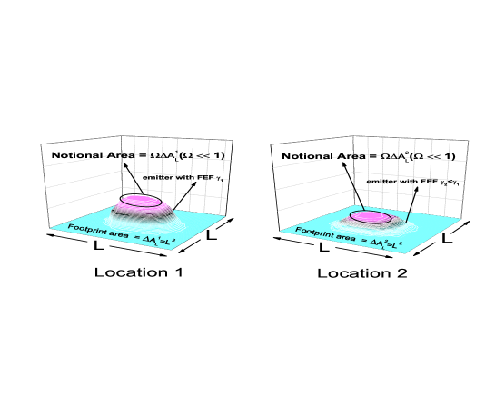
We remember that Eq. (10) considers negligible the total emission contribution where the FEF is effectively unity, i.e., at planar regions of footprint. For a plausible estimation of , which is expected to be much less than unit, we consider the following arguments: experimental values of macroscopic current density are often around mA/cm2. However, according to Dyke and Dolan DykeTrolan , a mid-range local current density might be around A/cm2. This suggest that typical experimental notional area efficiencies might be around (this is confirmed in Sec.III.3 for our electrostatic simuations with hemispherical tips). Then, in this work, we investigate a device with an array of isolated nanostructures, where . Finally, the sum in Eq. (10) is taken over the macroscopic substrate footprint area of the emitter, , which contains a number of locations, , each one with footprint of area as shown in Fig. 1. The macroscopic current density can also be written as:
| (11) |
where is the notional area efficiency, has already been defined in Section 1, has a similar meaning as that of in Eq. (6). In this work, it is assumed that , so that . Finally, the kernel current density for the (image-force-related) SN barrier is given by
| (12) |
In Ref.deAssis22015 , the dependency between and was evaluated for for the case in which corresponds to a family of Gaussian distributions, with different values of the variance . The results indicated a slight decreasing change in the slope of the FN plot, for large values of and . These non-linear behavior was not large enough to cause a failure of the orthodoxy test, nor was able to give rise to two intervals with well defined and different slopes. As it will be shown in the next section, the latter may appear in the present model under specific conditions of the bimodal distribution function, which includes the vales of and .
Nonlinear behavior in FN plots have been reported in several recent CFE experiments Li ; Patra ; Ahmed ; Zhang ; Li2 ; Lu ; JVSTB2003 , where the discussion of their results were based on the elementary FN equation. Moreover, we pondered that some of the results have showed do not pass the orthodoxy test, and cannot to be interpreted only on the light of the results of the present work (which consider only orthodox field emission), despite similar forms of FN plots have been obtained. For instance, in Ref.Li2 the field emission properties of “flexible SnO2 nanoshuttle” led to FN plots with a clear crossover presenting two quasi-linear sections. As pointed by Forbes Forbes1 , for both sections, as a consequence of the unorthodoxy emission (possible explanations include field-dependent changes in emitter geometry and/or changes in collective electrostatic screening effects), spurious FEF values have been found.
Ref.Lu analyzed the field electron emission properties of well-aligned graphitic nano-cones synthesized on polished silicon wafers. The authors have investigated how the difference between the values of corresponding to two types of emission sites on the LAFE surface affects the effective emission area for a given range of values. Unfortunately, some of their experimental outputs have shown also inconsistencies with the orthodox assumptions Forbes3 ; Forbes1 . For instance, consider the data shown in Fig. 2 of Ref.Lu together with the work function eV of graphitic nano-cones. For anodes with diameter mm, mm, mm and mm and low regime (where a sufficient linear FN plot is obtained), we find, respectively, the following corresponding values for the scaled barrier field [see Eq.(8)] and . The first value has been found for = mV-1, while the three further values were found for = mV-1. This suggests that, for all cases where non-linear behavior is observed in the corresponding FN plots, a closer investigation is required to provide a reliable interpretation of the results. In this specific study, this corresponds to the two smaller anodes. Moreover, for the larger anodes with nonuniform substrates, the orthodoxy test clearly fails, despite the linear behavior of the FN plots. Therefore, the corresponding FEFs indicated in these two cases and the corresponding emission areas extracted are questionable. Finally, is important to emphasize that, very recently, Forbes provided a simple confirmation that the SN barrier is a better model for actual conducting emitters than the usual triangular barrier ForbesIVNC2015 to extract the emission areas. This can be noticed for a tungsten emitter (X89) data from Dyke and Trolan DykeTrolan and independent assessment of emitter area made by electron microscopy.
III Results and Discussions
III.1 Formal area efficiency: role of and
Remembering that the formal area efficiency is an experimentally accessible measure of the fraction of the LAFE surface that is actually emitting electrons, let us explicitly indicate its dependency on in Eq.(11) by writing
| (13) |
After some manipulations using Eqs.(9-11) and Eqs.(4-10), the following expression can be written (see Appendix - A):
| (14) |
where
| (15) |
Based on the actual experimental FEF values Nilson2 , we fix , while is free to take different values. This is in accordance with the previous assumptions that the active LAFE emission sites fall into two classes, one of which is “more pointy” than the other, and hence has a higher FEF. Changes in , with the corresponding changes in , are restricted to the condition that the electric field over the LAFE device does not exceed a few V/nm, while other complicated effects (as destruction of the LAFE device due to thermal effects) have been neglected.
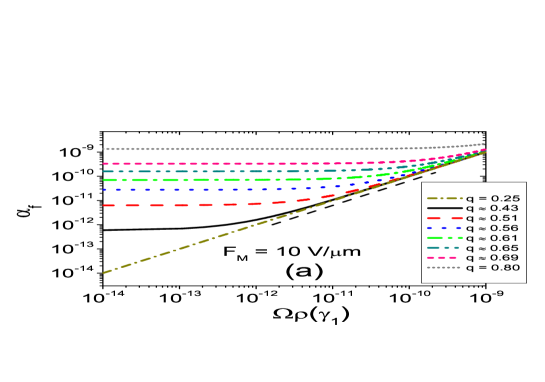
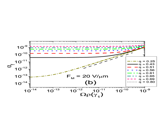
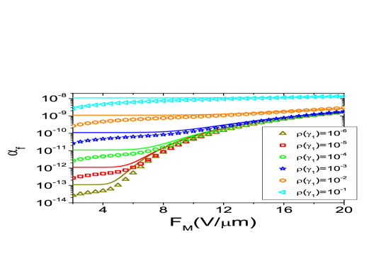
Eq.(14) makes it clear that depends on . This is illustrated in Fig. 2(a) that shows, for several values of and for a typical value m, the behavior of as changes from to . The values of were computed by using Eqs.(14) and (15). For small values of (e.g., ), Fig. 2(a) shows that assumes, approximately, the same values of . In this limit, for m, and the only emitting spots on the LAFE surface are those with for all . This behavior is not observed for other values of and smaller values of , when the contribution of the regions for the electron emission become relevant as compared with regions. However, for larger values of , again the main emitting spots that contribute to are those with . In this case, the curve bends upwards and , which is observed as long as is not so close to 1. Finally, when the limit is approached, the regions with contribute to for almost all range of values of . It is important to stress that, as increases, a more uniform LAFE surface is built, with the presence of second-scale structures presenting close values of . The results shown in Fig. 2(b) indicate the behavior of at a larger value m. In this case, the results suggest that, for values of close to unity, the regions of the LAFE surface also contribute to for low values of . As will be discussed in the next subsection, when and is not so close to 1, depends on leading to nonlinear behavior in the corresponding FN plots. Before discussing the behavior of the FN plots, we investigate how is related with when both and are kept fixed.
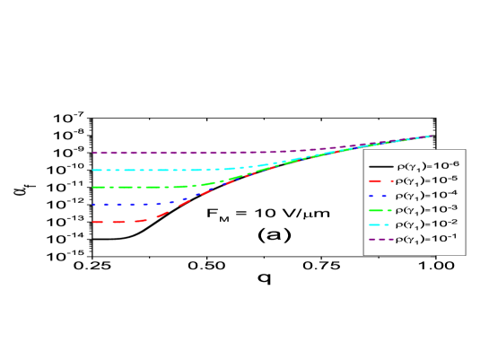
Fig. 3(a) shows the behavior of as a function of for several values of and m. It’s possible to observe that, for higher values of , the wider is the interval where has a weak dependency on . In this regime, and, again, the regions which contributes to are only those with . After the plateau, which increases as increases, is expected to depends more strongly on . Fig. 3(b) illustrate the behavior for m. Now the plateau disappears for small values of and, in this regime, depends on in the entire displayed range. For larger values of , e.g. , the plateau region is restored. However, even in this range of , it’s possible to observe the weak dependency between and for larger values of .
III.2 Fowler-Nordheim plots
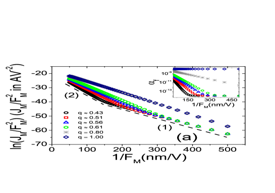
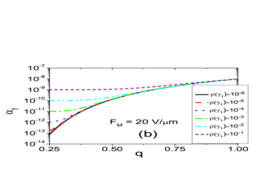
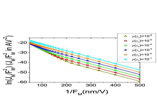
We now discuss the effect of the FEF distribution on the FN plots. Fig.4(a) presents FN plots for several values of and a fixed , for the typical range of applied field 2 V/ m 20 V/m in CFE for vacuum nano-electronic technologies. It’s possible to identify two well separated regions with a sharp crossover between two different slopes and , when . In Table I, we list all pertinent values resulting from the analysis presented in Figs. 4(a) and 4(b). In the limit, the two slope pattern becomes less evident and linear behavior prevails. The inset of Fig.4(a) shows the behavior of as a function of , indicating that the nonlinear behavior on the FN plots is related to the dependency between and . In the low macroscopic electric field limit, it’s possible to identify, for , that presents a constant behavior, suggesting that the main emitting spots correspond to the regions with . In the high limit, depends exponentially on , as expected from Eqs. (14) and (15). Here, the regions with contribute to the field electron emission.
Our results for the relation between the and [see Eqs. (10) and (12)] add valuable insights to the discussion about the physical reasons that are responsible for the crossover phenomenon in FN plots. Previous works suggest that the weak nonlinear dependency in FN plots could be traced back to a simple relation to , namely , where has a weak dependency on but is strongly influenced by the LAFE geometry deAssis12015 ; deAssis22015 . This effect provides a more general method for a reliable assessment of the characteristic FEF from FN plots. A good approximation for the true FEF was derived in deAssis12015 ; deAssis22015 , which leads to
| (16) |
where was introduced in Eq. (8). Under orthodox emission conditions the situation is that, if does not depend on , generally over-predicts by approximately 5%. As anticipated in the Sec.II, is verified for practical circumstances ForbesSlope . The correction , which was introduced very recently by one of authors deAssis12015 ; deAssis22015 , accounts for a nonlinear relationship between the macroscopic and the characteristic local current density, both of which are accessible experimentally.
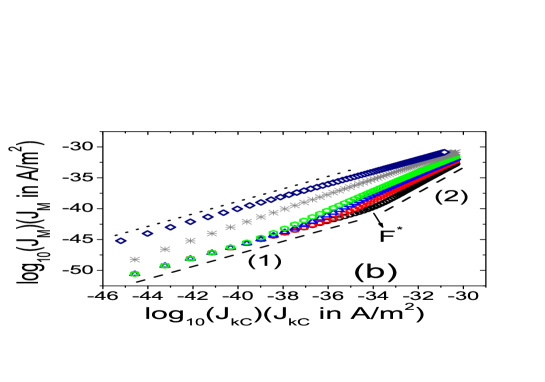
In Fig.4(b), we illustrate the behavior of as a function of for the same parameters used in Fig.4(a). We clearly identify that the same two slope patterns in the FN plots is observed for the dependency between and . Thus, it’s convenient to define and so that
| (17) |
where and correspond to the approximations for the characteristic FEF using the slopes and , respectively. The results in Fig.4(b), together with Eqs. (13)-(15), suggest that:
| (18) |
and
| (19) |
Here denotes the value of the electric field at the crossover point that separates the regions with two different slopes in FN plots as indicated in Fig.4(b). In Appendix - B, we provide detailed derivation of the expressions that allow to extract the parameter “” from similar nonlinear FN plots in orthodox CFE experiments. “” is a function of , , as well as of the local work function that through the exponent .
The results in Table I indicate that in the low regime. The slope provides information on the characteristic FEF, . In this regime, the results reinforce the interpretation that CFE is orthodox, as confirmed by the extracted value [see Eq.(8) of this work, and Table 2 in Ref. Forbes1 , for eV]. On the other hand, for high values of , Table I indicates , which means that, besides the regions with , the regions with also contributes in a significant way to . This suggests an important result that might be suitable for experimental observation: when in the corresponding range of , the slope provides information regarding the macroscopic FEF, . A good estimate of the real characteristic FEF would be , for . For this ansatz, the errors do not exceed , as indicated in Table I for . More interestingly, the values of shown on Table I (extracted from the range ), confirm that the emission is also orthodox.
At this point, we emphasize the importance of measuring . To see this, let us consider two different LAFE devices: (i) the first one is characterized by uniform local FEFs with (and ); (ii) the second one is composed by regions with two distinct FEFs values, namely and () and . The device (i) represents an ideal homogeneous array composed by the same second-scale structures. Device (ii) represents an array where most of the second-scale structures are characterized by , but there is a small probability to find regions with , as already discussed in the characterization of a non-uniform LAFE surface. Both corresponding FN plots are shown in Fig. 3(a), but the two curves are actually indistinguishable. However, the results in the inset show that, while is independent of in case (i), does depend on for the device (ii). These observations culminate with the following conclusions: although FN plots present the same behavior for two distinct LAFE surfaces, in case (i) the corresponding slope provides the correct value of the characteristic FEF. On the other hand, the device (ii) has characteristic FEF . Thus, the linear aspect of the FN plot does not mean, necessarily, that the area of emission does not depend on the macroscopic field. Indeed, the results in the inset of Fig. 3(a) for device (ii) hints at change in the value of by, at least, two orders of magnitude. Moreover, despite the linear aspect and the orthodox CFE, the FN slope can not measure, necessarily, the characteristic FEF, . This reflects the importance of measure , so that suggests this behavior. Finally, we remark that if for a given range in CFE experiments, it just indicates that does not depends (or weakly depends) on the in that range.
III.3 Application to Isolated Nanopost Field Emitters (with )
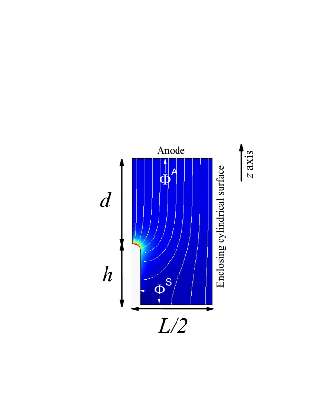
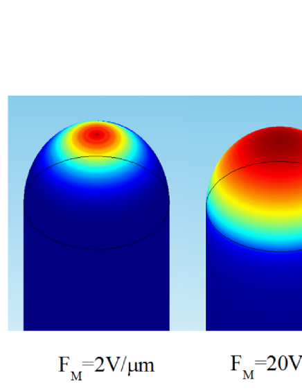
In this section, the validity of the former analysis is compared with those for a structured emitter. We assume the single emitters as structures shown in Fig.5, which are usual representations of nano-emitters as a hemisphere on a conducting cylindrical post CNT1 ; CNT2 ; Cole ; MC . We solve numerically the Laplace’s equation, in a three dimensional domain, using an array of conducting nano-emitters with large apex radii ( nm) but different heights, and (), which are associated to the FEFs and , respectively. In our analysis, we fix , with and . This corresponds, in our simulations, to nanostructures with aspect ratios () close to and , respectively. The latter are compatible with field emission displays where electrons are emitted from micron-sized tips PatFE . The electric potential distribution on the integration domain was calculated using a Finite Element Method scheme (software COMSOL v4.3b). This allows to calculate the electric field distribution over the LAFE device, as well as the local emitting current density using Eq.(9). We consider the same work function, eV used in the previous section. Fig. 5 shows the radial integration domain (emitting location) and the used boundary conditions for an idealized situation in which a single tip is placed in the center of a location. The line at the right side boundary generates an enclosing cylindrical surface (ECS) when it is rotated by around the position where the left boundary lies. In this way, the electric field component normal to this plane is locally zero everywhere. Since a similar geometry may be found in the neighboring locations, with the exception that the tips do not necessarily lie in the corresponding location centers, the resulting field may be distorted as a consequence of the superposition of individual field at each location. Thus, there is an overall screening effect inside each ECS. In this work we use and , so that the screening is negligible (the emitters can be considered as isolated) and the field lines can be considered parallel and vertically aligned FAD . The electric potential of the anode at the top boundary guarantees electric field intensity equal to at the boundary. Moreover, the emitter surface and the bottom boundary of the cell are grounded (=0). For the purpose of calculating area efficiencies, we assume that each post-like emitter has “footprints” of area .
The macroscopic current density was calculated as follow:
| (20) |
where the sum is computed over all spherical cap surface area and and correspond to probabilities to found a location of LAFE that contains a nanostructure with characteristic FEF and , respectively. In this case, may changes essentially for two reasons: (i) the emitters with FEFs contribute to the overall current; (ii) the notional area on each emitter increases slowly as increases, as shown in Fig.6. To illustrate this dependency, we have computed the normalized local current density map () at macroscopic electric fields 2V/m and 20V/m. In fact, it is possible to observe a clear increase of the notional area of a single nano-emitter, as first suggested by Abott and Henderson Abott in 1939. In Fig.7, we show a comparison for the dependency of as a function of for two methodologies: the one based on Eqs.(14) and (15), and that obtained by solving Laplace’s equation. In the latter, using the dimensions previously discussed, . Moreover, the results suggest that is weakly dependent on . Then, in Eq.(10) we have used the reasonable proportionality , which means to use in Eq.(14). It’s possible to observe the good agreement between two results. A small deviation occurs in low regime, which can be justified because the emitting area of a single tip structure grows very slowly as the macroscopic electric field increases (see Fig.6). However, an important result is that this very subtle effect does not affect the form of FN plots. Fig.8 shows the nonlinear behavior of FN plots for actual emitters, considering and , showing the excellent agreement with the results from Eqs.(14) and (15).
IV Conclusions
In this work, we present a theoretical explanation for the crossover in the behavior of the FN plots, commonly found for large area field emitters with irregular morphology. The latter is assumed to lead to a more prominent emitting locations with FEFs distributed approximately as a bimodal distribution. Our results suggest an orthodox field electron emission for two quasi-linear sections of FN plots as the formal area efficiency is the sole cause of the crossover, in a typical range V/m. For such situations, we propose a physically relevant ansatz leading to the interpretation of the slopes in FN plots as a function of the and asymmetry parameters characterizing . Finally, the results from solution of Laplace’s equation for an array of conducting nano-emitters supports our theoretical assumptions regarding the information provided by FN plots, which can be tested if CFE experiments are orthodox.
Acknowledgements
The authors acknowledge the financial support of the Brazilian agency CNPq. TAdA thanks R. G. Forbes for fruitful discussions and for calling attention to Ref.[6].
APPENDIX
IV.1 Derivation of
According to Eqs.(10) and (5), the macroscopic current density for a LAFE with two prominent emitter locations can be written as
| (21) |
We emphasize that, in our theory, represents the footprint area of th post-like emitter. represents the corresponding notional emission area. Then, using Eq.(9) (for ), assuming that is weakly field dependent, and , Eq.(21) becomes
| (22) |
Once the term appears in both terms, we take into account that , to simplify Eq.(22) to
| (23) |
where is given by Eq.(12). Then, making use of the notation introduced in Eq.(13), the formal area efficiency can be given by:
| (24) |
A generalization of Eq.(24) that consider a LAFE with a larger number of tips types, i.e. with (j=1,…,n), can be easily derived, leading to
| (25) |
where and .
IV.2 Extraction of parameter “” from nonlinear FN plots in orthodox CFE experiments
If CFE experiments are orthodox and the FN plots present two clear-cut quasi-linear sections, it’s possible to provide an estimation of the parameter “” defined in Eq.(5). Let the macroscopic electric field at the crossover point that separates the regions with two different slopes be noted by , as illustrated in Fig.4(b). At this point, it is expected that the contribution for macroscopic current density from the locations with FEF is the same as those from the locations with FEF . This lead to
| (26) |
From Eq.(26), it’s possible to write the product as
| (27) |
where . From the expressions for the two distinct slopes in the same corresponding FN plot, and , it’s possible to write
| (28) |
| (29) |
References
References
- (1)
- (2) E. McCarthy, S. Garry, D. Byrne, E. McGlynn, and J.-P. Mosnie, J. of Appl. Phys. 110, 124324 (2011).
- (3) C. A. Spindt, J. Appl. Phys. 39, 3504 (1968).
- (4) O. Gröening, R. Clergereaux, L.-O. Nilsson, P. Ruffieux, P. Gröning, and L. Schlapbach, CHIMIA Int. J. Chem. 56, 553 (2002).
- (5) M. T. Cole, K. B. K. Teo, O. Gröening, L. Gangloff, P. Legagneux, and W. I. Milne, Sci. Rep. 4, 4840 (2014).
- (6) M. Cahay, W. Zhu, S. Fairchild, P.T. Murray, T. C. Back, and G. J. Gruen, Appl. Phys. Lett.108, 033110 (2016).
- (7) C. C. Lauritsen, “Electron Emission from metals in intense electric fields”, Ph.D. thesis (1929).
- (8) R. G. Forbes, J. H. B. Deane, A. Fischer, and M. S. Mousa, Jordan J. of Phys. 8, 125 (2015).
- (9) R. G. Forbes, Proc. R. Soc. A 469, 20130271 (2013).
- (10) R. G. Forbes, Nanotech. 23, 288001 (2012).
- (11) T. A. de Assis, Sci. Rep. 5, 10175 (2015).
- (12) T. A. de Assis, J. Vac. Sci. Technol. B 33, 052201 (2015).
- (13) R.G. Forbes and J.H.B. Deane, Proc. R. Soc. Lond. A 463, 2907 (2007).
- (14) R.G. Forbes, J. Vac. Sci. Technol. B 26, 788 (2008).
- (15) E. L. Murphy, E. H. Good, Phys. Rev. 102, 1464 (1956).
- (16) J.H.B. Deane and R.G. Forbes, J. Phys. A: Math. Theor. 41, 395301 (2008).
- (17) R.G. Forbes, Nanotech. 23, 095706 (2012).
- (18) R. G. Forbes, J. Vac. Sci. Technol. B 2, 209 (2008).
- (19) R. G. Forbes. Appl. Phys. Lett. 92, 193105 (2008).
- (20) W.P. Dyke, and J.K. Trolan, Phys. Rev. 89, 799 (1953).
- (21) S. Li, K. Yu, Y. Wang, Z. Zhang, C. Song, H. Yin, Q. Ren, and Z. Zhu, CrystEngComm, 15, 1753 (2013).
- (22) R. Patra et al., J. Appl. Phys. 116, 164309 (2014).
- (23) A. A. Al-Tabbakh, M. A. More, D. S. Joag, I. S. Mulla, and V. K. Pillai, ACSNANO, 4 5585 (2013).
- (24) X.-Q. Zhang, J.-B. Chen, C.-W. Wang, A.-Z. Liao, and X.-F. Su, Nanotech. 26 175705 (2015).
- (25) J. Li, M. Chen, S. Tian, A. Jin, X. Xia, and C. Gu, Nanotech. 22 505601 (2011).
- (26) X. Lu, Q. Yang, C. Xiao, and A. Hirose, J. of Phys. D: Appl. Phys. 39 3375 (2006).
- (27) J. P. Singh, F. Tang, T. Karabacak, T.-M. Lu, and G.-C. Wang, J. Vac. Sci. Technol. B 22, 1048 (2004).
- (28) R.G. Forbes, “Improved methods of extracting area-like information from CFE current-voltage data”, IVNC (2015).
- (29) L. Nilsson, O. Gröening, P. O. Gröening, O. Kuettel, and L. Schlapbach, J. Appl. Phys. 90, 768 780 (2001).
- (30) R. G. Forbes, A. Fischer, and M. S. Mousa, J. Vac. Sci. Technol. B 31(2), 1 (2013).
- (31) Y.Wei, P. Liu, H.-Y. HAO, and S.-S. Fan, Field emission electronic device, US 8450920 B2 (2010).
- (32) D. W. Kang, and S. Suh, J. Appl. Phys., 96, 5234 (2004).
- (33) W. Zeng, G. Fang, N. Liu, L. Yuan, X. Yang, S. Guo, D. Wang, Z. Liu, X. Zhao, Diamond and Related Materials, 18 1381 (2009).
- (34) F. R. Abbott, and J. E. Henderson, Phys. Rev., 56 113 (1939).
- (35) F. F. Dall’Agnol, and D. den Engelsen, Nanosc. and Nanotech. Lett., 5, 329 (2013).