Transmission gaps from corrugations
Abstract
A model including a periodically corrugated thin layer with GaAs substrate is employed to investigate the effects of the corrugations on the transmission probability of the nanostructure. We find that transmission gaps and resonant tunneling domains emerge from the corrugations, in the tunneling domains the tunneling peaks and valleys result from the boundaries between adjacent regions in which electron has different effective masses, and can be slightly modified by the layer thickness. These results can provide an access to design a curvature-tunable filter.
PACS Numbers: 73.50.-h, 73.20.-r, 03.65.-w, 02.40.-k
I INTRODUCTION
With the advent and development of nanostructure technology, a variety of nanostructures with complex geometries were successfully fabricated, such as corrugated semiconductor films Prinz2001 ; Prinz2006 ; Li2008 ; Turner2010 ; Mutilin2014 ; Zhang2015 , rolled-up nanotubes Schmidt2001 ; Prinz2007 ; LiuF2007 ; Naumova2009 ; Froeter2013 ; Dastjerdi2015 , Möbius stripes Tanda2002 ; Yoon2009 ; Monceau2012 , peanut-shaped polymers Onoe2003 ; Onoe2007 ; Onoe2008 ; Onoe2012 ; Onoe2015 . These successes in experiment found the basis of the emerging nanoelectronics. In the two-dimensional (2D) reduced systems, the dynamics of confined electron is affected by the surface curvature. As an important consequence, the geometric potential induced by the curvature appears in the effective surface quantum equation Ferrari2008 ; BJensen2009a ; Ortix2011 ; Wang2014 by the thin-layer quantization procedure HJensen1971 ; Costa1981 ; Costa1982 ; Wang2016 . In the procedure, a squeezing potential is introduced to accomplish the reduction of the number of the spatial variables of the curved systems. Physically, the squeezing process is probably severe and breaks with the natural limits set by the uncertainty principle. Even so, the present quantization scheme can be safely applied to study the motion of confined electron when the quantum excitation energies in the normal direction are raised far beyond those in the tangential direction. Actually, the thin-layer quantization method has successfully been employed to calculate the band-structure of real systems Aoki2001 ; Fujita2005 ; Koshino2005 , determine the localized surface states in geometrically deformed quantum systems Goldstone1992 ; Cantele2000 ; Encinosa2003 ; Taira2007a ; Taira2007b ; BJensen2009b ; Ortix2010 , and study the transport properties of electron confined in the systems with complex geometries Marchi2005 ; Zhang2007 ; Cuoghi2009 ; Shima2009 . Furthermore, the experimental evidences for the geometrical effects of the curved surface have been presented, such as the realization of an optical analog of the curvature-induced geometric potential Szameit2010 , the observation of the influence of geometry on proximity effect Kim2012 and the observation of Riemannian geometrical effects on electronic states Onoe2012 . In other words, the geometrical deformation can be concluded as the presence of geometric potential in the dimensionally reduced quantum equation.
In the same vein, the advent and development of nanostructures have clearly led to a frontier field in 2D semiconductor research Chang1992 ; Buot1993 ; Kushwaha1994 ; Lamberti2004 ; Jiang2012 ; XuS2015 . It is now possible to design and fabricate materials with prescribed electronic and photonic properties by artificial band-gap engineering. In order to satisfy the requirement of the development of nanoelectronics, theoretical physicists have tried to study the effects of the geometrical deformation on the tunneling rate Encinosa2000 , the electrical resistivity Ono2009 ; Ono2010a and the persistent current Taira2010 ; Shima2012 . Moreover, on the basis of the geometric potential, quantum-electromechanical circuits Blencowe2004 ; Chaplik2004 ; Xiang2013 and thin film transistors Amalraj2014 have been proposed.
In fact, over the years, the electronic properties of the periodically curved surface have been the subject of active studies, both theoretical and experimental, due to the demand in understanding the physics involved and its great application potential. The ability to confine electron nearly to 2D regions on nanostructures has given a new impetus toward understanding the physics of reduced dimensionality systems. An important property of nanostructures is how their geometries affect their behaviors. Usually, one thinks of geometrical effects being connected primarily with the physical size and barrier configuration that define the confining region of the nanostructure.
In the present study, we consider a model Encinosa2000 (shown in Fig. 1) which contains two barriers and a well, the well is fabricated as a periodically corrugated thin layer. In the model, denotes free electron beam source, is a barrier with width , is a corrugated thin layer with width , is the other barrier with width , and denotes a drain, from left to right.

The double barriers resonant tunneling structure is a typical microstructure that has been the focus of many investigations Li1990 ; Chen1991a ; Chen1991b ; Kane1992 ; Doering1992 ; Nguyen2013 . In the present model, the corrugations are employed to provide transmission gaps and resonant tunneling domains, the double barriers and the boundaries between adjacent regions, in which electron has different effective masses, are adopted to generate the tunneling peaks and valleys in the tunneling domains. The theoretical basis is that when the spatial dimension is reduced to a scale being comparable with the de Broglie wavelength of electron in the vicinity of Fermi energy in the model, the wave nature of electron is expected to play an increasingly important role in transport properties.
This paper is organized as follows. In Sec. II, we briefly review the effective quantum equation for electron confined in a periodically corrugated layer by the thin-layer quantization scheme, and analyze the curvature-induced geometric potential. In Sec. III, we obtain a new geometric potential by the extended thin-layer quantization scheme, and also analyze the thickness-modified geometric potential. In Sec. IV, we investigate the effects of the corrugations, double barriers and boundaries on transmission probability. Finally in Sec. V the conclusions are given.
II Quantum dynamics of a particle confined on a periodically corrugated surface
A 2D curved surface embedded in the usual three-dimensional (3D) space can be parametrized by , where and are the curvilinear coordinate variables over . With respect to and , two unit basis vectors and over are defined by and , respectively. By introducing a curvilinear coordinate variable along the direction normal to , a 3D subspace consisting of points near to and on can be described by , where is the unit basis vector perpendicular to , with the definition . In , the covariant components of the metric tensor are defined by . On , the covariant components of the reduced metric tensor are determined by . The relationships between and are
| (1) |
and , , where denotes the matrix transpose, is the Weingarten curvature matrix
| (2) |
wherein are the coefficients of the second fundamental form, . By means of , the mean curvature is and the Gaussian curvature , and then the relation between and is with .
Basing on the above mathematical formula, we can confine a free electron on a curved surface by the thin-layer quantization scheme HJensen1971 ; Costa1981 , the effective surface Schrödinger equation is obtained as
| (3) |
where is the geometric potential
| (4) |
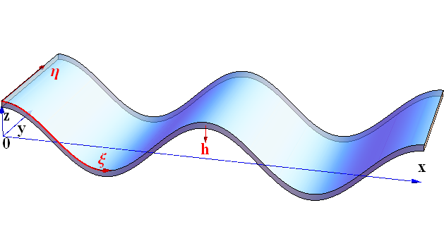
Practically, nanocorrugated thin-films are often found in nanomaterial experiments. For the sake of simplicity, a curved surface shown in Fig. 2 is considered. It is corrugated along the direction of with period , amplitude , but is flat along that of . In the Monge form, can be described as
| (5) |

According to the procedure mentioned above, from Eq. (5) we obtain three unit basis vectors and corresponding three derivative elements
| (6) |
respectively, with
| (7) |
Subsequently, we obtain and
| (8) |
the Weigarten curvature matrix
| (9) |
and
| (10) |
where . In the above calculated process, the factor , the mean curvature and the Gaussian curvature can be given as
| (11) |
Consequently, the expected Schrödinger equation (3) is
| (12) |
where denotes the effective mass of electron, and is the geometric potential
| (13) |
These results are the same as those given by S. Ono and H. Shima Ono2009 . The quantum motion in the normal direction is neglected, because the introduced squeezing potential raises the quantum excitation energies in normal direction far beyond those in tangential direction HJensen1971 ; Costa1981 .
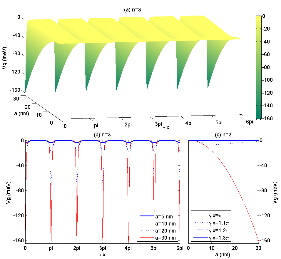
As the central result of the thin-layer quantization scheme, the geometric potential appears in the expectant quantum equation. With and ( is the effective mass of electron in GaAs substrate) the geometric potential shown in Fig. 3 is a function of and , where denotes the period number of the corrugations in , is the mass of a free electron. As observed in Fig. 3 (a), the dependence of deviates considerably from a cosinusoidal surface, whereas the surface corrugation is exactly cosinusoidal. It is shown in Fig. 3 (b) that the downward peaks are formed at , here the height of the surface is either maximum or minimum . The amplitude of the peaks grows sharply with increasing that is highlighted in Figs. 3 (b) and (c). As a consequence, we can provide a list of attractive potential wells by introducing corrugations, tune their depths by , and design their number by .
III The modification of the layer thickness to the geometric potential
Really, the corrugated layer has certain thickness. The thickness effects on the effective quantum equation (12) can be investigated by the extended thin-layer quantization scheme Wang2016 . In the present model the thickness effects on the kinetic term can be neglected, because the thickness lengthens the displacement of electron across the layer very slightly, whereas a thickness-modified geometric potential can be given as
| (14) |
where denotes the layer thickness sketched in Fig. 4 and is the geometric potential (13). The second term on the right hand side of Eq. (14) attributes to the layer thickness. It needs to notice that must be less than the minimum curvature radius on . For an arbitrary point on , there is only one principle curvature , the corresponding curvature radius is
| (15) |
It is obvious that the minimum curvature radius is at . When , at new points (they have a uniform distance to ) ”” is , the corresponding mean curvature becomes . In order to avoid the trouble, we primitively define ranging between and .
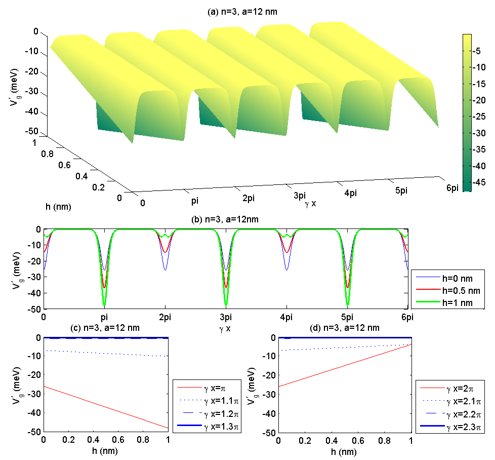
As an important result for the extended thin-layer quantization scheme Wang2016 , the modification of the layer thickness is included in , as a function of and , described in Fig. 5 with and . As mentioned above, the downward peaks are still formed at . However, there is a change shown in Fig. 5 (a), the downward peaks at grow with increasing , but those at dwarf, that is highlighted in Figs. 5 (b), (c) and (d).
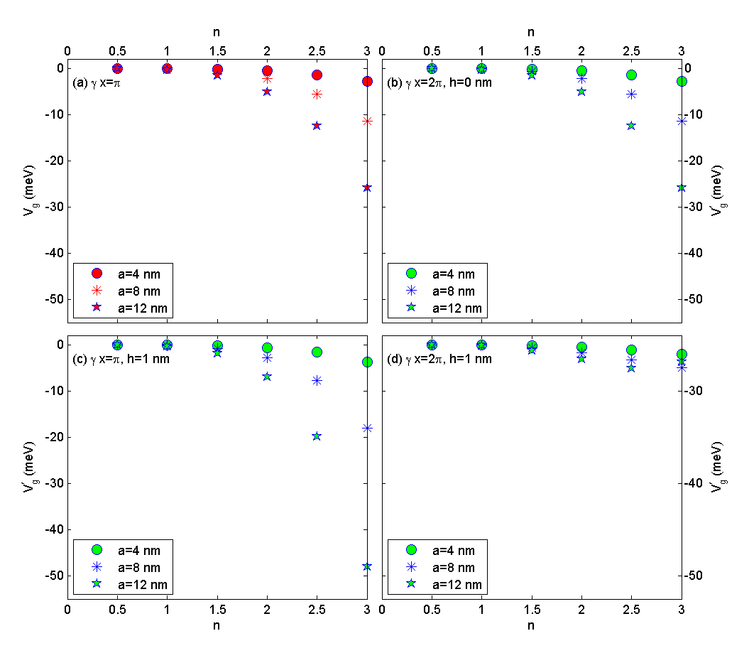
The scales of and are substantially influenced by described in Figs. 6 (a) and (b), the larger the period number , the deeper the peaks at . Obviously, as shown in Figs. 6 (c) and (d), evidently deepens the peaks at , but remarkably shallows those at . In other words, we can adjust the discrepancy between adjacent wells by depositing the layer thickness finely.
IV Transmission probability in the periodically corrugated thin layer
IV.1 Transmission probability
According to Eq. (12), with the limit the quantum equation for an electron in the model depicted in Fig. 1 can be
| (16) |
where (the effective mass of electron in GaAs substrate) if and otherwise, if and otherwise, is a wave function, is the energy with respect to and is
| (17) |
wherein is the geometric potential (13) and denotes milli electron volts. When the effects of the layer thickness are considered, should be replaced by in Eq. (14).
With the help of the transfer matrix technique Ando1987 , instead of dealing with continuous variations of in , we split up into segments, in each segment can be regarded as a constant. And then let us assume will be a sequence small segments, one segment () and one segment (). It is straightforward to obtain that the total number of segments is , that of boundaries is . For an arbitrary segment, the th region, in which the wave function can be given by
| (18) |
where
| (19) |
wherein is the reduced Planck’s constant, is the effective mass for electron at the middle point in the th region, is a constant, . For the wave function (18), it is particular that the curvilinear coordinate variable as a function of has the derivative form if and otherwise.
On account of the continuities of and at each boundary, we can determine and in Eq. (18) by the following multiplication
| (20) |
where
| (21) |
with
| (22) |
As , the equation (20) becomes
| (23) |
where
| (24) |
Without any loss of generality, we assume that in the model under study is an electron source consisting of free electrons, and is a drain. Using the plane wave approximation, the wave function in can be
| (25) |
and in
| (26) |
where and are the coefficients of reflection and transmission, respectively. In the case of , , and , we can obtain the transmission amplitude and the transmission probability as
| (27) |
and
| (28) |
respectively.
IV.2 Numerical results and analysis
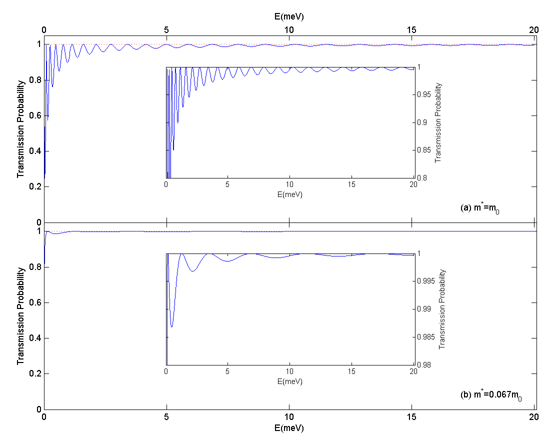
In this subsection, we will investigate how the corrugations affect the transmission probability by the transfer matrix method. Before beginning the investigation, we briefly analyze the effects of other components in the model on the transmission probability. The effective masses of electron in the model are closely related to the resonant tunneling peaks as shown in Figs. 7. When the effective mass is less, the number of the peaks is less, their amplitudes smaller. These results are highlighted in the insets in Fig. 7.
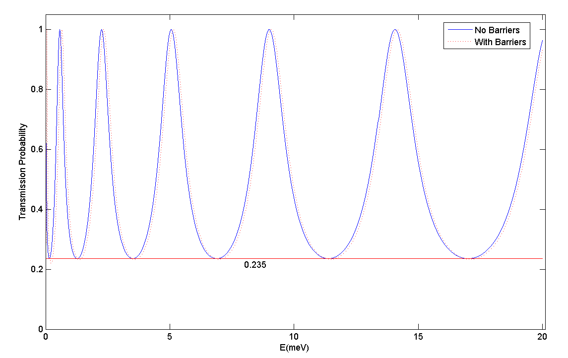
In the case of the model with in and otherwise, the two boundaries between and , and are essential to influence the transmission probability. In response to the boundaries, the amplitudes of the tunneling peaks considerably grow shown in Fig. 8. In other words, these peaks are mostly provided by the continuities of and , the contributions of the double barriers could be neglected. It is worth noticing that the peaks almost reach , the valleys are about . Physically, the peaks occur when the length of strictly equals integer multiple times of a half wave length of electron, the bottom of the valleys is eventually determined by the ratio of the effective masses in and (or ).
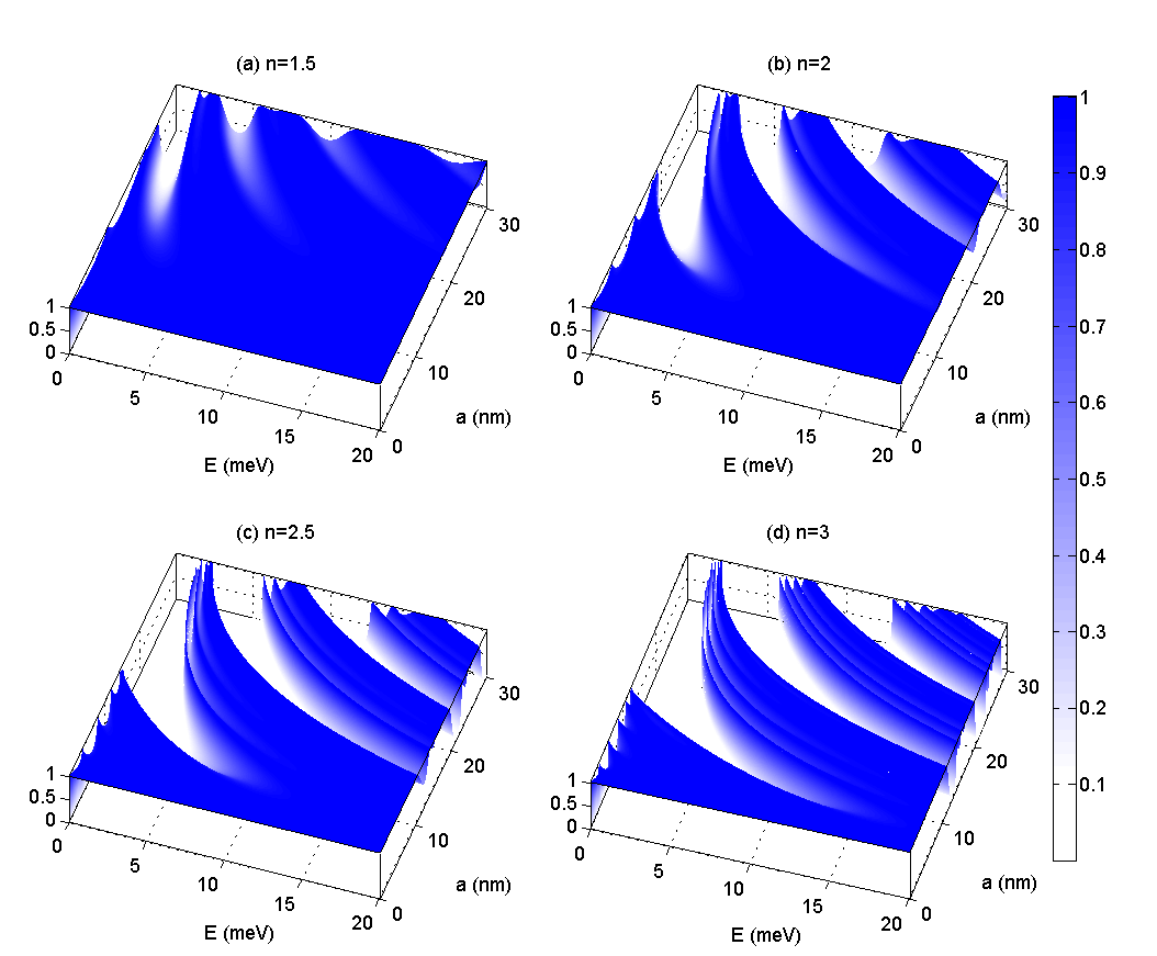
In a special case, the model without the double barriers, with in all regions, in and otherwise, transmission gaps Khelif2003 ; Chen2009a ; Chen2009b ; Lu2012 ; XuY2015 and resonant tunneling domains LiuXW1993 ; Guo1998 ; Zeng1999 ; Xu2014 ; Pham2015 appear in the present system shown in Fig. 9. The presence of the transmission gaps is the most fascinating finding in this study. It is readily proved that the widths of the transmission gaps grow with increasing the corrugation amplitude . The cause is that the larger the distances between adjacent wells in the geometric potential , the less the communication or coupling between adjacent wells LiuXW1994 . As periodical corrugations presented in , the factor in Eq. (16) is a function of as , in must be replaced by
| (29) |
According to this integral, the distance between adjacent wells naturally grows with increasing the corrugation amplitude. Another aspect of the transmission probability is that the transmission gaps become wider when is larger with a fixed , the tunneling domains do narrower correspondingly. The reason is that the more the number of the wells, the stronger their reflections. The resonant tunneling domains are formed essentially by the coupling between adjacent wells, with respect to resonant energy domains LiuXW1994 ; Lu2013 . As an application potential, the transmission gaps mean that electron is mostly reflected, but the tunneling domains do that electron can readily pass.
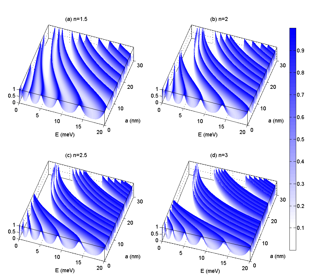
In the considered case, the model with in fabricated by GaAs substrate and otherwise, with in Eq. (17), the transmission probability as a function of and is described in Fig. 10 for (a) , (b) , (c) and (d) . In striking contrast to Fig. 9, Fig. 10 shows that tunneling peaks and valleys evidently occur in the tunneling domains. Significantly, the transmission gaps are still kept. That is to say that the boundaries and the double barriers cannot considerably influence the transmission gaps, but they construct the tunneling peaks and valleys in the tunneling domains, especially when the amplitude is small. This result can be directly manifested by that the bottom of the valleys is still a certain constant at , which well agrees with that described in Fig. 8. Additionally, it is worthwhile to note that the number of the tunneling peaks in each of the tunneling domains is equivalent to that of the wells in the geometric potential.
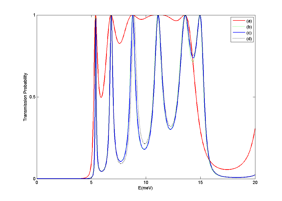
In order to highlight the influences of the double barriers and the layer thickness to the transmission probability, in the case of and , the transmission probability as a function of is plotted in Fig. 11. Strikingly, it shows that the transmission gaps are mostly provided by the corrugations. The peaks and valleys in the tunneling domains are mainly formed by the boundaries between adjacent regions in which electron has different masses. And the boundaries can make the transmission gaps flatter. Trivially, the double barriers and the layer thickness affect on the valleys at a small scale.
V Conclusions
A particular component of the considered model is the presence of periodically corrugated thin layer. The corrugated deformation contributes the geometric potential , a sequence attractive potential wells, to the electron across the corrugated layer. The number of wells is determined by the period number of the corrugations as . The depth of wells grows with increasing the amplitude of the corrugations. Approximately, the geometric potential can be roughly equivalent to a sequence square potential wells. The square wells can be structured by introducing periodically magnetic fields. In terms of the magnetic field, the filter designed for electron with certain energy is the vector-tunable filter Anna2009 . By means of the surface curvature, the filter structured for electron with certain energy can be named as a curvature-tunable filter. When the layer thickness is considered, the potential should be replaced by , which includes the modification given by the layer thickness . For the sake of application, the difference between adjacent wells can be controlled by depositing the layer thickness.
The most fascinating finding in the present study is the presence of the transmission gaps and resonant tunneling domains resulting from the periodic corrugations. In the gaps electron is mostly reflected, in the tunneling domains electron readily passes. Additionally, in the resonant tunneling domains the resonant splitting peaks and valleys essentially attribute to the boundaries between adjacent regions in which electron has different effective masses, and is slightly influenced by the layer thickness . These results can provide a considerable access for experimenters to fabricate nanoelectronic device. As a potential application, we can control the widths of the transmission gaps by the amplitude and period number of the corrugations, design the resonant splitting peaks and valleys by depositing different materials in adjacent regions with certain thickness. Experimentally, the nanocorrugated thin films can be obtained by the detachment method Prinz2001 ; Prinz2006 . The corrugated nanofilms fabricated from narrow-gap and gapless semiconductors can be the most promising objects for experiment. In real physical experiments, Coulomb electron interaction, spin-orbital coupling, screening effects and atomic structure need to be considered for two-dimensional curved systems. These interesting questions need to be studied further.
Acknowledgments
This work is supported by the National Natural Science Foundation of China (under Grant Nos. 11047020, 11404157, 11347126, 11304138, 11275097, 11475085, 11535005).
References
- (1) V. Ya. Prinz, D. Grützmacher, A. Beyer, C. David, B. Ketterer, and E. Deckardt 2001 Nanotechnology 12 399
- (2) V. Ya. Prinz, 2006 Phys. Status Solidi B 243 3333
- (3) X. Li 2008 J. Phys. D: Appl. Phys. 41 193001
- (4) A. M. Turner, V. Vitelli, and D. R. Nelson 2010 Rev. Mod. Phys. 82 1301
- (5) S. V. Mutilin, R. A. Soots, A. B. Vorob’ev, D. G. Ikusov, N. N. Mikhailov, and V. Ya. Prinz 2014 J. Phys. D: Appl. Phys. 47 295301
- (6) Y. Zhang, Z. Yan, K. Nan, D. Xiao, Y. Liu, H. Luan, H. Fu, X. Wang, Q. Yang, J. Wang, W. Ren, H. Si, F. Liu, L. Yang, H. Li, J. Wang, X. Guo, H. Luo, L. Wang, Y. Huang, and A. Rogers 2015 Pro. Nat. Acad. Sci. 112 11757
- (7) O. G. Schmidt and K. Eberl 2001 Nature 410 168
- (8) A. B. Vorob’ev, K.-J. Friedland, H. Kostial, R. Hey, U. Jahn, E. Wiebicke, Ju. S. Yukecheva, and V. Ya. Prinz 2007 Phys. Rev. B 75 205309
- (9) J. Zang, M. Huang, and F. Liu 2007 Phys. Rev. Lett. 98 146102
- (10) E. V. Naumova, V. Ya. Prinz, S. V. Golod, V. A. Seleznev, R. A. Soots, and V. V. Kubarev 2009 J. Opt. A: Pure Appl. Opt. 11 074010
- (11) P. Froeter, X. Yu, W. Huang, F. Du, M. Li, I. Chun, S. H. Kim, K. J. Hsia, J. A. Rogers, and X. Li 2013 Nanotechnology 24 475301
- (12) M. H. T. Dastjerdi, M. Djavid, and Z. Mi 2015 Appl. Phys. Lett. 106 021114
- (13) S. Tanda, T. Tsuneta, Y. Okajima, K. Inagaki, K. Yamaya, and N. Hatakenaka 2002 Nature 417 397
- (14) Z. S. Yoon, A. Osuka, and D. Kim 2009 Nature Chem. 1 113
- (15) P. Monceau 2012 Adv. Phys. 61 325
- (16) J. Onoe, T. Nakayama, M. Aono, and T. Hara 2003 Appl. Phys. Lett. 82 595
- (17) J. Onoe, T. Ito, S.-I. Kimura, K. Ohno, Y. Noguchi, and S. Ueda 2007 Phys. Rev. B 75 233410
- (18) Y. Toda, S. Ryuzaki, and J. Onoe 2008 Appl. Phys. Lett. 92 094102
- (19) J. Onoe, T. Ito, H. Shima, H. Yoshioka, and S.-I. Kimura 2012 Europhys. Lett. 98 27001
- (20) H. Masuda, J. Onoe, and H. Yasuda 2015 Carbon 81 842
- (21) G. Ferrari, and G. Cuoghi 2008 Phys. Rev. Lett. 100 230403
- (22) B. Jensen, and R. Dandoloff 2009 Phys. Rev. A 80 052109
- (23) C. Ortix, and J. van den Brink 2011 Phys. Rev. B 83 113406
- (24) Y.-L. Wang, L. Du, C.-T Xu, X.-J. Liu, and H.-S. Zong 2014 Phys. Rev. A 90 042117
- (25) H. Jensen, and H. Koppe 1971 Ann. Phys. (N.Y.) 63 586
- (26) R. C. T. da Costa 1981 Phys. Rev. A 23 1982
- (27) R. C. T. da Costa 1982 Phys. Rev. A 25 2893
- (28) Y.-L. Wang, and H.-S. Zong 2016 Ann. Phys. (N.Y.) 364 68
- (29) H. Aoki, M. Koshino, D. Takeda, H. Morise, and K. Kuroki 2001 Phys. Rev. B 65 035102
- (30) N. Fujita and O. Terasaki 2005 Phys. Rev. B 72 085459
- (31) M. Koshino and H. Aoki 2005 Phys. Rev. B 71 073405
- (32) J. Goldstone and R. L. Jaffe 1992 Phys. Rev. B 45 14100
- (33) G. Cantele, D. Ninno, and G. Iadonisi 2000 Phys. Rev. B 61 13730
- (34) M. Encinosa and L. Mott 2003 Phys. Rev. A 68 014102
- (35) H. Taira and H. Shima 2007 J. Phys.: Conf. Ser. 61 1142
- (36) H. Taira and H. Shima 2007 Surf. Sci. 601 5270
- (37) B. Jensen 2009 Phys. Rev. A 80 022101
- (38) C. Ortix and J. van den Brink 2010 Phys. Rev. B 81 165419
- (39) A. Marchi, S. Reggiani, M. Rudan, and A. Bertoni 2005 Phys. Rev. B 72 035403
- (40) E. Zhang, S. Zhang, and Q. Wang 2007 Phys. Rev. B 75 085308
- (41) G. Cuoghi, G. Ferrari, and A. Bertoni 2009 Phys. Rev. B 79 073410
- (42) H. Shima, H. Yoshioka, and J. Onoe 2009 Phys. Rev. B 79 201401(R)
- (43) A. Szameit, F. Dreisow, M. Heinrich, R. Keil, S. Nolte, A. Tünnermann, and S. Longhi 2010 Phys. Rev. Lett. 104 150403
- (44) J. Kim, V. Chua, G. A. Fiete, H. Nam, A. H. MacDonald, and C.-K. Shih 2012 Nature Phys. 8 464
- (45) L. L. Chang and L. Esaki 1992 Phys. Today 45(10) 36
- (46) F. A. Buot 1993 Phys. Rep. 234 73
- (47) M. S. Kushwaha, P. Halevi, G. Martínez, L. Dobrzynski, and B. Djafari-Rouhani 1994 Phys. Rev. B 49 2313
- (48) C. Lamberti 2004 Surf. Sci. Rep. 53 1
- (49) X.-W. Jiang, S.-S. Li, and L.-W. Wang 2012 Solid-State Electron 68 56
- (50) S. Xu, Z. Yan, K.-I. Jang, W. Huang, H. Fu, J. Kim, Z. Wei, M. Flavin, J. McCracken, R. Wang, A. Badea, Y. Liu, D. Xiao, G. Zhou, J. Lee, H. U. Chung, H. Cheng, W. Ren, A. Banks, X. Li, U. Paik, R. G. Nuzzo, Y. Huang, Y. Zhang, and J. A. Rogers 2015 Science 347 154
- (51) M. Encinosa 2000 IEEE Trans. Electron Devices 47 878
- (52) S. Ono and H. Shima 2009 Phys. Rev. B 79 235407
- (53) S. Ono and H. Shima 2010 Physica E 42 1224
- (54) H. Taira and H. Shima 2010 J. Phys.: Condens. Matter 22 075301
- (55) H. Shima 2012 Phys. Rev. B 86 035415
- (56) M. Blencowe 2004 Phys. Rep. 395 159
- (57) A. V. Chaplik and R. H. Blick 2004 New J. Phys. 6 33
- (58) Z.-L. Xiang, S. Ashhab, J. Q. You, and F. Nori 2013 Rev. Mod. Phys. 85 623
- (59) R. Amalraj and S. Sambandan 2014 J. Appl. Phys. 116 164507
- (60) Y. P. Li, A. Zaslavsky, D. C. Tsui, M. Santos, and M. Shayegan 1990 Phys. Rev. B 41 8388
- (61) L. Y. Chen and C. S. Ting 1991 Phys. Rev. B 43 4534
- (62) L. Y. Chen and C. S. Ting 1991 Phys. Rev. B 43 2097
- (63) C. L. Kane and M. P. A. Fisher 1992 Phys. Rev. B 46 15233
- (64) C. R. Doering and J. C. Gadoua 1992 Phys. Rev. Lett. 69 2318
- (65) H. S. Nguyen, D. Vishnevsky, C. Sturm, D. Tanese, D. Solnyshkov, E. Galopin, A. Lemaître, I. Sagnes, A. Amo, G. Malpuech, and J. Bloch 2013 Phys. Rev. Lett. 110 236601
- (66) Y. Ando and T. Itoh 1987 J. Appl. Phys. 61 1497
- (67) A. Khelif, B. Djafari-Rouhani, J. O. Vasseur, and P. A. Deymier 2003 Phys. Rev. B 68 024302
- (68) X. Chen, L.-G. Wang, and C.-F. Li 2009 Phys. Rev. A 80 043839
- (69) X. Chen and J.-W. Tao 2009 Appl. Phys. Lett. 94 262102
- (70) W.-T. Lu, S.-J. Wang, W. Li, Y.-L. Wang, and H. Jiang 2012 Physica B 407 918
- (71) Y. Xu, Y. He, and Y. Yang 2015 Physica B 457 188
- (72) X.-W. Liu and A. P. Stamp 1993 Phys. Rev. B 47 16605
- (73) Y. Guo, B.-L. Gu, Z.-Q. Li, J.-Z. Yu, and Y. Kawazoe 1998 J. Appl Phys. 83 4545
- (74) Z. Y. Zeng, L. D. Zhang, X. H. Yan, and J. Q. You 1999 Phys. Rev. B 60 1515
- (75) Y. Xu, Y. He, and Y. Yang 2014 Appl. Phys. A 115 721
- (76) C. H. Pham and V. L. Nguyen 2015 J. Phys.: Condens. Matter 27 095302
- (77) X.-W. Liu and A. P. Stamp 1994 Phys. Rev. B 50 1588
- (78) W.-T. Lu, W. Li, Y.-L. Wang, H. Jiang, and C.-T. Xu 2013 Appl. Phys. Lett. 103 062108
- (79) L. Dell’Anna and A. De Martino 2009 Phys. Rev. B 80 155416